Solutions - Loop Gain an... Analog Control Systems
高性能视频放大器AD8010使用手册说明书

REV.AInformation furnished by Analog Devices is believed to be accurate and reliable. However, no responsibility is assumed by Analog Devices for its use, nor for any infringements of patents or other rights of third parties which may result from its use. No license is granted by implication oraAD8010One Technology Way, P.O. Box 9106, Norwood, MA 02062-9106, U.S.A.Tel: 781/329-4700World Wide Web Site: 200 mA Output Current High Speed AmplifierCONNECTION DIAGRAMS8-Lead DIP and SOIC87651234NC = NO CONNECTNC –IN +IN NC +V S OUT NC–V S AD801016-Lead Wide Body SOIC161514131234NC = NO CONNECTNC –IN +IN NC +V S OUT NC –V S 12111095678NC NC NC NC NC NC NC NCAD8010V IN+5V–5V75⍀75⍀AD8010R TR GR FR SFigure 1.Video Distribution AmplifierPRODUCT DESCRIPTIONThe AD8010 is a low power, high current amplifier capable of delivering a minimum load drive of 175 mA. Signal performance such as 0.02% and 0.03° differential gain and phase error is maintained while driving eight 75 Ω back terminated video lines.The current feedback amplifier features gain flatness to 60 MHz and –3 dB (G = +1) signal bandwidth of 230 MHz and only requires a typical of 15.5 mA supply current from ±5 V supplies.These features make the AD8010 an ideal component for Video Distribution Amplifiers or as the drive amplifier within high data rate Digital Subscriber Line (VDSL and xDSL) systems.The AD8010 is an ideal component choice for any application that needs a driver that will maintain signal quality when driving low impedance loads.The AD8010 is offered in three package options: an 8-lead DIP,16-lead wide body SOIC and a low thermal resistance 8-lead SOIC, and operates over the industrial temperature range of –40°C to +85°C.FEATURES200 mA of Output Current 9 ⍀ LoadSFDR –54 dBc @ 1 MHzDifferential Gain Error 0.04%, f = 4.43 MHz Differential Phase Error 0.06؇, f = 4.43 MHzMaintains Video Specifications Driving Eight Parallel 75 ⍀ Loads0.02% Differential Gain 0.03؇ Differential Phase0.1 dB Gain Flatness to 60 MHz THD –72 dBc @ 1 MHz, R L = 18.75 ⍀IP3 42 dBm @ 5 MHz, R L = 18.75 ⍀1 dB Gain Compression 21 dBm @ 5 MHz, R L = 100 ⍀230 MHz –3 dB Bandwidth, G = +1, R L = 18.75 ⍀800 V/s Slew Rate, R L = 18.75 ⍀25 ns Settling Time to 0.1%Available in 8-Lead DIP, 16-Lead Wide Body SOIC and Thermally Enhanced 8-Lead SOIC APPLICATIONSVideo Distribution Amplifier VDSL, xDSL Line Driver Communications ATEInstrumentation查询AD8010供应商捷多邦,专业PCB打样工厂,24小时加急出货AD8010–SPECIFICATIONS(@ +25؇C, V S = ؎5 V, G = +2, R L = 18.75 ⍀, R S+ = 150 ⍀, R F = R G = 604 ⍀ (R-16), R F = R G = 562 ⍀ (N-8), R F = R G = 499 ⍀ (R-8). T MIN = –40؇C, T MAX = +85؇C unless otherwise noted)M odel Conditions Min Typ Max Units DYNAMIC PERFORMANCE–3 dB Bandwidth G = +1, V OUT = 0.2 V p-p180230MHzG = +2, V OUT = 0.2 V p-p130190MHz0.1 dB Bandwidth V OUT = 0.2 V p-p3060MHzLarge Signal Bandwidth V OUT = 4 V p-p90MHz Peaking V OUT = 0.2 V p-p, < 5 MHz0.02dB Slew V OUT = 2 V p-p800V/µs Rise and Fall Time V OUT = 2 V p-p 2.0ns Settling Time0.1%, V OUT = 2 V p-p25ns NOISE/HARMONIC PERFORMANCEDistortion V OUT = 2 V p-p2nd Harmonic 1 MHz–73dBc5 MHz–58dBc10 MHz–53dBc10 MHz, R L = 39 Ω–67dBc20 MHz–44dBc3rd Harmonic 1 MHz–77dBc5 MHz–63dBc10 MHz–57dBc10 MHz, R L = 39 Ω–63dBc20 MHz–50dBcIMD 5 MHz ∆f = 10 kHz–73dBc IP3 5 MHz42dBm1 dB Gain Compression 5 MHz21dBmInput Noise Voltage f = 10 kHz2nV√Hz Input Noise Current f = 10 kHz, +In3pA√Hzf = 20 kHz, –In20pA√HzDifferential Gain f = 4.43 MHz, R L = 150 Ω0.02%f = 4.43 MHz, R L = 18.75 Ω0.02%Differential Phase f = 4.43 MHz, R L = 150 Ω0.02Degreesf = 4.43 MHz, R L =18.75 Ω0.03Degrees DC PERFORMANCEInput Offset Voltage512mVT MIN–T MAX15mV Offset Drift10µV/°C Input Bias Current (–)10135µAT MIN–T MAX200µA Input Bias Current (+)612µAT MIN–T MAX20µA INPUT CHARACTERISTICSInput Resistance+Input125kΩ–Input12.5ΩInput Capacitance 2.75pF Common-Mode Rejection Ratio V CM = ±2.5 V5054dB Input Common-Mode Voltage Range±2.5V Open Loop Transresistance V OUT = ±2.5 V300500kΩT MIN–T MAX250kΩOUTPUT CHARACTERISTICSOutput Voltage SwingR L = 18.75 Ω±2.1±2.5V R L = 150 Ω±2.7±3.0V Output Current R L = 9 Ω175200mA Short-Circuit Current240mA Capacitive Load Drive40pF POWER SUPPLYOperating Range±4.5±6.0V Quiescent Current15.517mAT MIN to T MAX20mA Power Supply Rejection Ratio+V S = +4 V to +6 V, –V S = +5 V6066dB+V S = +5 V, –V S = –4 V to –6 V5056dBAD8010ABSOLUTE MAXIMUM RATINGS 1Supply␣Voltage . . . . . . . . . . . . . . . . . . . . . . . . . . . . . . . .12.6␣V Internal␣Power␣Dissipation 2Plastic␣Package (N) . . . . . . .Observe Power Derating Curves Small␣Outline␣Package (R) . .Observe Power Derating Curves Wide Body SOIC (R-16) . . . .Observe Power Derating Curves Input Voltage (Common-Mode) . . . . . . . . . . . . . . . . . . . .±V S Differential␣Input␣Voltage . . . . . . . . . . . . . . . . . . . . . .±1.2␣V Output Short Circuit Duration.␣. . . . . . . . . . . . . . . . . . . . . .Observe Power Derating Curves Storage Temperature Range N, R . . . . . . . .–65°C to +125°C Operating Temperature Range (A Grade) . . .–40°C to +85°C Lead Temperature Range (Soldering␣10␣sec) . . . . . . . .+300°CNOTES1Stresses above those listed under Absolute Maximum Ratings may cause perma-nent damage to the device. This is a stress rating only; functional operation of the device at these or any other conditions above those indicated in the operational section of this specification is not implied. Exposure to absolute maximum rating conditions for extended periods may affect device reliability.2Specification is for device in free air:8-Lead Plastic Package: θJA = 90°C/Watt 8-Lead SOIC Package: θJA = 122°C/Watt 16-Lead SOIC Package: θJA = 73°C/WattAMBIENT TEMPERATURE – ؇C–50M A X I M U M P O W E R D I S S I P A T I O N – W a t t s–40–30–20–100102030405060708090Figure 2.Plot of Maximum Power Dissipation vs. TemperatureCAUTIONESD (electrostatic discharge) sensitive device. Electrostatic charges as high as 4000V readily accumulate on the human body and test equipment and can discharge without detection.Although the AD8010 features proprietary ESD protection circuitry, permanent damage may occur on devices subjected to high energy electrostatic discharges. Therefore, proper ESD precautions are recommended to avoid performance degradation or loss of functionality.ORDERING GUIDEModelTemperature Range Package Description Package Options AD8010AN –40°C to +85°C 8-Lead Plastic DIP N-8AD8010AR –40°C to +85°C 8-Lead Plastic SOICSO-8AD8010AR-16–40°C to +85°C16-Lead Wide Body SOIC R-16AD8010AR-REEL REEL SOIC 13" REEL AD8010AR-REEL7REEL SOIC 7" REEL AD8010AR-16-REEL REEL SOIC 13" REEL AD8010AR-16-REEL7REEL SOIC7" REELMAXIMUM POWER DISSIPATIONThe maximum power that can be safely dissipated by the AD8010 is limited by the associated rise in junction tempera-ture. The maximum safe junction temperature for plasticencapsulated devices is determined by the glass transition tem-perature of the plastic, approximately +150°C. Temporarily exceeding this limit may cause a shift in parametric perfor-mance due to a change in the stresses exerted on the die by the package. Exceeding a junction temperature of +175°C for an extended period can result in device failure.While the AD8010 is internally short circuit protected, this may not be sufficient to guarantee that the maximum junction temperature (+150°C) is not exceeded under all conditions. To ensure proper operation, it is necessary to observe the maximum power derating curves.AD8010dG (%)/d – Degrees60300.130.01P E R C E N T A G E O F U N I T S0.020.030.040.050.060.070.080.090.100.110.12504020100Figure 3.Distribution of Differential Gain (dG) andDifferential Phase (d φ); R L = 18.75 ΩFREQUENCY – MHzH A R M O N I C D I S T O R T I O N – d B cFigure 4.Harmonic Distortion vs. Frequency; G = +2Figure 5.Gain Flatness vs. Frequency Over Temperature (–40°C to +85°C)NUMBER OF VIDEO LOADS0.050.041624681012140.030.020.01D I F F E R E N T I A L G A I N – %10.100.080.060.040.02D I F FE R E N T I A LP H A S E – D e g r e e sFigure 6.Differential Gain and Phase vs. Number of Video Loads Over Temperature (–40°C to +85°C); f = 4.43 MHzFigure 7.Two-Tone, 3rd Order IMD Intercept vs.Frequency; G = +2, RL = 18.75 Ω6.56.46.36.26.16.05.95.85.75.65.5FREQUENCY – MHzG A I N F L A T N E S S – d BFigure 8.Gain Flatness vs. Frequency vs. Number of Video Loads–Typical Performance CharacteristicsAD8010FREQUENCY – MHzI N T E R M O D U L A T I O N D I S T O R T I O N – d B mFigure 9.Intermodulation DistortionP OUT – dBm–35–75–105–1012–8T O T A L H A R M O N I C D I S T O R T I O N – d B c–6–4–2246810–45–55–85–95–65Figure 10.Total Harmonic Distortion vs. P OUT ; G = +2FREQUENCY – MHz21–7N O R M A L I Z E D G A I N – d B0–1–6–2–3–4–5 Figure 11.Small Signal Closed-Loop Frequency Response; R L = 18.75ΩFREQUENCY – MHz10123456789–10–90P M E A S U R E – d B m–50–60–70–80–30–40–20Figure 12. Multitone Distortion; R L = 100 ΩLOAD – ⍀–55–60–65–70–75–80–85–9015100200300400500H A R M O N I C D I S T O R T I O N – d B cFigure 13.Harmonic Distortion vs. LoadFigure 14.Closed-Loop Frequency Response vs. Number of Video LoadsAD8010FREQUENCY – MHz–10–200.035000.1P S R R – d B110100–30–40–80–50–60–70Figure 15.PSRR vs. FrequencyFREQUENCY – MHz0.15001C L O S ED -L O O P O U T P U T RE S I S T A N C E – ⍀1010031010031103.110.310.1Figure 16.Closed-Loop Output Resistance vs. FrequencyFREQUENCY – MHz21N O R M A L I Z E D G A I N – d B–1–2–7–3–4–5–60Figure rge Signal Frequency Response; V O = 2 V p-pFREQUENCY – MHz0.15001C M R R – d B101000–10–100–20–30–40–50–60–70–80–90Figure 18.CMRR vs. FrequencyFREQUENCY – Hz3160.31610k1G100kT R A N S R E S I S T A N C E – k ⍀1M 10M 100M10031.6103.16190P H A S E – D e g r e e s451000Figure 19.Transresistance and Phase vs. Frequency;R L = 18.75 ΩFREQUENCY – MHz0.1N O R M A L I Z E D G A I N – d B1003.02.0–7.01.00.0–1.0–2.0–3.0–4.0–5.0–6.0Figure rge Signal Frequency Response; V O = 4 V p-pAD8010Figure 21.Small-Signal Pulse Response; G = +1Figure 22.Small-Signal Pulse Response; G = +2, –110010FREQUENCY – Hz 1k 1010010k 100k 1M 1I N P U T V O L T A G EN O I S E – n V / H z10MFigure 23.Input Voltage Noise vs. FrequencyV O L T SFigure rge-Signal Pulse Response; G = +1Figure 25.Large-Signal Pulse Response; G = +2, –1100101FREQUENCY – HzI N P U T C U R R E N T N O I S E – P A H z1000Figure 26.Input Current Noise vs. FrequencyAD8010V O L T SFigure 27.Overdrive Recovery; G = +6OVERDRIVE RECOVERYOverdrive of an amplifier occurs when the output and/or input range are exceeded. The amplifier must recover from this over-drive condition. As shown in Figure 27, the AD8010 recovers within 35 ns from negative overdrive and within 75 ns from positive overdrive.THEORY OF OPERATIONThe AD8010 is a current feedback amplifier optimized for high current output while maintaining excellent performance with respect to flatness, distortion and differential gain/phase. As a video distribution amplifier, the AD8010 will drive up to 12parallel video loads (12.5 Ω) from a single output with 0.04%differential gain and 0.04° differential phase errors. This means that, unlike designs with one driver per output, any output is a true reflection of the signal on all other outputs.The high output current capability of the AD8010 also make it useful in xDSL applications. The AD8010 can drive a 12.5 Ωsingle-ended or 25 Ω differential load with low harmonic distor-tion. This makes it useful in designs that utilize a step-up trans-former to drive a twisted-pair transmission line.To achieve these levels of performance special precautions with respect to supply bypassing are recommended (Figure 29). This configuration minimizes the contribution from high frequency supply rejection to differential gain and phase errors as well as reducing distortion due to harmonic energy in the power supplies.R S – ⍀205C A P A C I T I V E L O AD – p F1015Figure 28.Capacitive Load Drive vs. Series Resistor for Various GainsDriving Capacitance LoadsThe AD8010 was designed primarily to drive nonreactive loads.If driving loads with a capacitive component is desired, best frequency response is obtained by the addition of a small series resistance as shown in Figure 28. The inset figure shows the optimum value for R SERIES vs. capacitive load. It is worth noting that the frequency response of the circuit when driving large capacitive loads will be dominated by the passive roll-off of R SERIES and C L.LAYOUT CONSIDERATIONSThe specified high speed performance of the AD8010 requires careful attention to board layout and component selection.Proper R F design techniques and low-pass parasitic component selection are necessary.The PCB should have a ground plane covering all unused por-tions of the component side of the board to provide low imped-ance path. The ground plane should be removed from the area near the input pins to reduce the parasitic capacitance.Figure 29.Standard Noninverting Closed-Loop Configura-tion with Recommended Bypassing TechniqueThe standard noninverting closed-loop configuration with the recommended power supply bypassing technique is shown in Figure 29. Ferrite beads (Amidon Associates, Torrance CA,Part Number 43101) are used to suppress high frequency power supply energy on the DUT supply lines at the DUT. C1 and C2each represent the parallel combination of a 47 µF (16 V) tanta-lum electrolytic capacitor, a 10 µF (10 V) tantalum electrolytic capacitor and a 0.1 µF ceramic chip capacitor. Connect C1from the +V S pin to the –V S pin. Connect C2 from the –V S pin to signal ground.The feedback resistor should be located close to the inverting input pin in order to keep the parasitic capacitance at this node to a minimum. Parasitic capacitances of less than 1 pF at the inverting input can significantly affect high speed performance.Stripline design techniques should be used for long traces (greater than about 3 cm). These should be designed with a characteristic impedance (Z O ) of 50 Ω or 75 Ω and be properly terminated at each end.AD8010APPLICATIONSVideo Distribution AmplifierThe AD8010 is optimized for the specific function of providing excellent video performance when driving multiple video loads in parallel. Significant power is saved and heat sinking is greatly simplified because of the ability of the AD8010 to obtain this performance when running on a ±5 V supply. However, due to the high currents that flow when driving many parallel video loads, special layout and bypassing techniques are required to assure optimal performance.When designing a video distribution amplifier with the AD8010, it is very important to keep in mind where the high (ac) currents will flow. These paths include the power supply pins of the chip along with the bypass capacitors and the return path for these capacitors, the output circuits and the return path of the output current from the loads.In general, any loops that are formed by any of the above paths should be made as small as possible. Large loops are both gen-erators and receivers of magnetic fields and can cause undesired coupling of signals that lowers the performance of the amplifier.Effects that have not been seen before in other op amp circuits might arise because of the high currents. Most op amp circuits output, at most, tens of milliamps and do not require extremely tight video specifications, while a video distribution amplifier can output hundreds of milliamps and require extremely low differential gain and phase errors.The bypassing scheme that is used for the AD8010 requires special attention. It was found that the conventional technique of bypassing each power pin individually to ground can have an adverse effect on the differential phase error of the circuit. The cause of this is attributed to the fact that there is an internal compensation capacitor in the AD8010 that is referenced to the negative supply.The recommended technique is to connect parallel bypass capacitors from the positive supply to the negative supply and then to bypass the negative supply to ground. For high fre-quency bypassing, 0.1 µF ceramic capacitors are recommended.These should be placed within a few millimeters of the power pins and should preferably be chip type capacitors.The high currents that can potentially flow through the power supply pins require large bypassing capacitors. These should be low inductance tantalum types and at least 47 µF. The ground side of the capacitor that bypasses the negative supply should be brought to a single point ground that is the common for the returns of the outputs.Figure 30 shows a circuit for making an N-channel video distri-bution amplifier. As a practical matter, the AD8010 can readily drive eight standard 150 Ω video loads. When driving up to 12video loads, there is minimal degradation in video performance.Another important consideration when driving multiple cables is the high frequency isolation between the outputs of the cables. Due to its low output impedance, the AD8010 achieves better than 46 dB of output-to-output isolation at 5 MHz driv-ing back terminated 75 Ω cables.Figure 30.An N-Channel Video Distribution Amplifier Using An AD8010.NOTE: Please see Figure 29 for Recommended Bypassing Technique.V L1L2LNAD8010Differential Line DriverTwisted pair transmission lines are more often being used for high frequency analog and digital signals. Over long distances,however, the attenuation characteristics of these lines can degrade the performance of the transmission system. To com-pensate for this, larger signals are transmitted, which after the attenuation, will still have useful signal strength.The high output current of two AD8010s can be used along with a transformer to create a high power differential line driver.The differential configuration effectively doubles the output swing, while the step-up transformer further increases the out-put voltage.In the circuit in Figure 31 the A device is configured as a gain-of-two follower, while the B device is a gain-of-two inverter.These will produce a differential output signal whose maximum value is twice the peak-to-peak value of the maximum output of one device. For this circuit a 12 V peak-to-peak output can be obtained.The op amps drive a 1:2 step-up transformer that drives a 100 Ω transmission line. Since the impedance reflected back to the primary varies as the square of the turns ratio, it will appear as 25 Ω at the primary. This source terminating resistor is split as a 12.4 Ω resistor at the output of each device.The circuit shown is capable of delivering 12 V p-p to the line and operates with a –3 dB bandwidth of 40 MHz. The peak current output of either op amp is 100 mA.Figure 31.High Output Differential Line Driver Using Two AD8010s.NOTE: Please see Figure 29 for Recommended Bypassing Technique.V ⍀AD8010 Closed-Loop Gain and BandwidthThe AD8010 is a current feedback amplifier optimized for usein high performance video and data acquisition applications.Since it uses a current feedback architecture, its closed-loop–3 dB bandwidth is dependent on the magnitude of the feed-back resistor. The desired closed-loop bandwidth and gain areobtained by varying the feedback resistor (R F) to set the band-width, and varying the gain resistor (R G) to set the desired gain.The characteristic curves and specifications for this data sheetreflect the performance of the AD8010 using the values of R Fnoted at the top of the specifications table. If a greater –3dB band-width and/or slew rate is required (at the expense of video per-formance), Table I provides the recommended resistor values.Figure 32 shows the test circuit and conditions used to produceTable I.Effect of Feedback Resistor Tolerance on Gain FlatnessBecause of the relationship between the 3 dB bandwidth and thefeedback resistor, the fine scale gain flatness will, to some ex-tent, vary with feedback resistor tolerance. It is therefore recom-mended that resistors with a 1% tolerance be used if it is desiredto maintain flatness over a wide range of production lots. Inaddition, resistors of different construction have different associ-ated parasitic capacitance and inductance. Metal-film resistorswere used for the bulk of the characterization for this data sheet.It is possible that values other than those indicated will be opti-mal for other resistor types.Quality of Coaxial CableOptimum flatness when driving a coax cable is possible onlywhen the driven cable is terminated at each end with a resistormatching its characteristic impedance. If the coax was ideal, then the resulting flatness would not be affected by the length of the cable. While outstanding results can be achieved using inex-pensive cables, it should be noted that some variation in flatness due to varying cable lengths may be experienced.OUTVFigure 32.Test Circuit for Table INOTES1VO= 0.2 V p-p for –3 dB Bandwidth.2VO= 2 V p-p for Slew Rate.3Bypassing per Figure 29.Table I.–3 dB Bandwidth and Slew Rate vs. Closed-Loop Gain and Resistor ValuesPackage: N-8Closed-Loop–3 dB BW Slew Rate Gain R F (⍀)R G (⍀)(MHz) (V/s) +1453∞285900+2374374255900+534886.6200800+1056261.9120550 Package: R-16Closed-Loop–3 dB BW Slew Rate Gain R F (⍀)R G (⍀)(MHz) (V/s) +1412∞245900+2392392220900+539297.6160800+1060466.595550 Package: SO-8Closed-Loop–3 dB BW Slew Rate Gain R F (⍀)R G (⍀)(MHz) (V/s) +1392∞345950+23743743051000+534886.62201000+1049954.9135650OUTLINE DIMENSIONSDimensions shown in inches and (mm).C 3208a –0–10/98P R I N T E D I N U .S .A .AD80108-Lead Plastic Mini-DIP(N-8)PLANE0.014 (0.356)0.045 (1.15)(2.54)BSC0.325 (8.25)0.300 (7.62)0.008 (0.204)8-Lead SOIC (SO-8)PLANE BSC ؇16-Lead Wide Body SOIC(R-16)PLANE0.0138 (0.35)(1.27)BSC0.0091 (0.23)。
GE Grid Solutions 8系列高级馈线控制器产品手册说明书

GEGrid Solutionsimagination at workInnovative Technology& Design• Advanced feeder One Box Solution for protection, control monitoring anddiagnostics of single/dual feeder applications Feeder and Bay Controller Solutions for Industrial and Utility ApplicationsThe Multilin™ 850 relay is a member of the Multilin 8 Series protective relay platform and has been designed for the management, protection and control of feeder applications. The Multilin 850 is used to provide primary (main) or backup protection for underground and overhead single or dual feeders for utility and industrial power networks.With 11 Switchgear control elements, fully configurable Single Line Diagram on a large color graphical display, 36 alarm integrated annunciator panel and 20 push buttons makes the 850 the ideal choice for bay control and protection as a “One Box Solution”.Designed with advanced communications options and detailed asset monitoring capabilities, the Multilin 850 provides advanced functionality, including high-performance protection, extensive programmable logic and flexible configuration capabilities. With support for industry leading communications protocols and technologies, the 850 provides easy integration into new or existing SCADA or DCS for enhanced situational awareness.Key Benefits• One Box Solution with advanced logic and configuration flexibility, providing primary or backup protection for up to 2 feeders or feeders with 2 sets of voltage inputs • User configurable Single Line Diagram on color display for local control, system status, and metering • Advanced breaker diagnostics with comprehensive fault and disturbance recording• Integrated arc flash detection using light sensors supervised by overcurrent to reduce incident energy and equipment damage • Advanced cyber security features including AAA, Radius, RBAC, and Syslog enabling NERC ® CIP requirements • Draw-out design simplifies testing, commissioning and maintenance, increasing process uptime • Patented environmental monitoring, providing visibility to changes in environmental conditions that can affect relay lifeApplications• Single/dual feeder applications for utility, oil & gas, mining & metals, process industry, commercial, and waste water segments • Fast protection pass enabling load shedding schemes • Reliable automatic bus transfer & autoreclose schemes • Bay controller for wide range of switchgear applications • High speed fault detection for arc flash mitigationMultilin 850WARRANTYYEAR850Multilin 850 OverviewThe Multilin 850 is an advanced feeder protection device designed for high performance, protection, control and monitoring of incoming and outgoing feeders.With up to 57 digital inputs and 22 digital outputs in a compact box, the 850 provides a versatile and cost effective control, protection, measurement & monitoring solution. Flexelements and Flexlogic enable users to customize schemes to meet a variety of applications.From dual main to main-standby configurations, the Multilin 850D delivers a more economical and reliable solution, enabling customers to reduce hardware requirements and simplify device integration, including safe and secure Wi-Fi communications for system configuration and diagnostics. Bay Controller/One Box SolutionThe 850 offers comprehensive switchgear control aided by a configurable Single Line Diagram & breaker control. A total of 10 switchgear elements can be displayed and 8 elements controlled. The integrated solution for protection, control, monitoring and diagnostics eliminates the need for other external devices thus offering an integrated solution for switchgear systems. The device supports 6 user programmable pages. The Multilin 850 is an integrated solution that performs protection, control & monitoring of assets, and ease of retrieval of fault & event records. Coordinating remotely with SCADA over multiple communication protocols gives the Multilin 850 an added advantage for fast and efficient management of fault isolation and service restoration.The Multilin 850 is a cost-effective retrofit solutions where individual components of protection, metering, control switches, annunciator & panel mimic can be replaced by only one relay. Switchgear Control and Configurable SLDThe Multilin 850 provides a configurable dynamic SLD up to six (6) pages for comprehensive switchgear control of up to 2 breakers and 9 disconnect switches; including interlocks. Up to 15 digital and metering status elements can be configured per SLD page. These can be configured to show breakers, switches, metering, and status items.Individual SLD pages can be selected for the default home screen pages. Automatic cycling through these pages can also be achieved through default screen settings.The provision of such powerful control and display capability within the relay (“One Box” concept) eliminates the need for external controls, switches and annunciation on the panel reducing equipment and engineering cost. Annunciator Panel and Virtual Push ButtonsThe Multilin 850 offers a configurable annunciator panel that can be constructed to show up to 36 alarms in either self-reset mode or latched mode per ISA 18.1 standard similar to a physical annunciator panel; eliminating the need for a physical one. This removes the need for additional programmable LEDs. The alarms can be displayed on the front panel in a configurable grid layout of 2x2 or 3x3.The Multilin 850 extends the local control functionalities with 20 virtual pushbuttons that can be assigned for various functions. Each programmable pushbutton has its own programmable LED which can be used to acknowledge the action taken by the tab pushbutton.With a fast protection pass, running every 2 msec, the 850 relay provides fast response to current, voltage, power, and frequency protection elements; helping reduce stress on assets. The Multilin 850 supports the latest communication protocols, including DNP, ModBus, IEC 60870-5-103, IEC 62439/PRP and IEC 61850; facilitating easy integration into new or existing SCADA/DCS networks.Functional Block Diagram850 Distribution FeederWith support for up to 8 CT inputs & 2 sets of 4 traditional VT inputs, the 850 can be used for 2 feeders or feeders with 2 sets of voltage inputs, simplifying system architectures and operational costs.The 850 offers redundancy with the same number of devices, enabling:Architecture Simplification - Reduced Number of Devices• Less capital cost • Less O&M costMean Time to Repair - Less than 15 minutes• Field swappable PSU • Draw out construction• Ready to consume service reportsExtended Asset and Relay Life• Built-in Environmental monitoring • Advanced breaker monitoring• TGFD and Cable incipient fault detection/locationSimplified Management - Platform Based Solution• Reduced training needs• Standardized part number across systems • Harmonized look and feel, operational experienceProtection & ControlAs part of the 8 Series family, the Multilin 850 provides superior protection and control. The 850 offers comprehensive protection and control solutions for incoming, outgoing bus-tie/bus-coupler feeders. It contains a full range of selectively enabled, self-contained protection and control elements.The voltage and frequency protection functions detect abnormal system conditions, potentially hazardous to the system. Some of these conditions may consist of over and undervoltage, over and underfrequency, and phase reversal.Fast UnderfrequencyThe 850 has an 8 stage Fast Underfrequency element that measures frequency by detecting the consecutive voltage zero crossings and measuring the time between them. The measured frequency has a range between 20 to 70 Hz. This is useful for performing fast load-shedding when frequency variations from unbalance conditions arise due to:• Inadequate load forecast or deficient generation capacity programming.• Busbars, generator group or interconnection feeders trip.• System splits into islands.FlexCurves™For applications that require greater flexibility, FlexCurves can be used to define custom curve shapes. These curves can be used to coordinate with other feeders to achieve fault selectivity.RTD ProtectionThe Multilin 850 supports up to 13 programmable RTD inputs that can be configured for an Alarm or Trip.The RTDs can be assigned to a group for monitoring ambient temperatures or any other desired temperature. The RTD voting option gives additional reliability to ignore and alarm for any RTD failures.Integrated Arc Flash ProtectionThe Multilin 8 Series supports an integrated arc flash module providing constant monitoring for an arc flash condition within the switchgear, motor control centers, or panelboards. With a 2ms protection pass, the 8 Series is able to detect light and overcurrent using 4 arc sensors connected to the relay. In situations where an arc flash/fault does occur, the relay is able to quickly identify the fault and issue a trip command to the associated breaker thereby reducing the total incident energy and minimizing resulting equipment damage.Self-monitoring and diagnostics of the sensors ensures the health of the sensors as well as the full length fiber cables. LEDs on the front panel display of the 850 can be configured to indicate the health of the sensorsand its connections to the relay.Dual feederRedundant feeder850WANT TO LEARN MORE?EXPLORE IN 3DMV SwitchgearMultilin 8 SeriesFast, reliable arc flash protection with integrated light based arc flash sensors. This delivers detection in as fast as 2 msec, reducing the costs associated with equipment damage and unplanned downtime.Inputs and OutputsThe 850 provides a max of 57 Digital inputs and 22 Digital outputs with an option for 7 Analog Outputs (dc mA), 4 Analog Inputs (dc mA), and 1 RTD input. The configurable analog inputs can be used to measure quantities fed to the relay from standard transducers. Each input can be individually set to measure 4-20 mA, 0-20 mA or 0-1 mA transducer signals.Advanced AutomationThe Multilin 850 incorporates advanced automation capabilities which exceed those found in most feeder protection relays. This reduces the need for additional programmable controllers or discrete control relays including programmable logic, communication, and SCADA devices. Advanced automation also enables seamless integration of the 850 into other protection or process systems (SCADA or DCS).FlexElements™FlexElement is a universal comparator, that can be used to monitor any (analog) actual value measured or calculated by the relay, or a net difference of any two analog (actual) values of the same type.The element can be programmed to respond either to a signal level or to a rate-of-change (delta) over a pre-defined period of time.This can be used to generate special protection or monitoring functions which allow the user to flag a user-defined abnormality to give better visibility to a certain condition.FlexLogic™FlexLogic is the powerful programming logic engine that provides the ability to create customized protection and control schemes, minimizing the need for and associated costs of auxiliary components and wiring. Using FlexLogic, the 850 can be programmed to provide the required tripping logic along with custom scheme logic for feeder control interlocking schemes with adjacent protection (for example, preventing sympathetic tripping of healthy feeders), and dynamic setting group changes.Breaker Health MonitoringThe breaker is monitored by the relay not only for detection of breaker failure, but also for the overall “breaker health” which includes:• Breaker close and breaker open times • Trip circuit monitoring • Spring charging time • Per-phase arcing current • Trip countersAll algorithms provide the user with the flexibility to set up initial breaker trip counter conditions and define the criteria for breaker wear throughouta number of set points.Breaker Health Reporting assists Condition-Based Maintenance and savings in Operational CostsMonitoring & DiagnosticsThe Multilin 850 includes high accuracy metering and recording for all AC signals. Voltage, current, and power metering are built into the relay as a standard feature. Current and voltage parameters are available as total RMS magnitude, and as fundamental frequency magnitude and angle.Environmental MonitoringThe 850 has an Environmental Awareness Module (EAM) to record environmental data over the life of the product. The patented module measures temperature, humidity, surge pulses and accumulates the events every hour in pre-determined threshold buckets over a period of 15 years. This data can be retrieved using the EnerVista Setup Software. This report helps identify the operating condition of the installed fleet so that remedial action can be taken.850Environmental health report is available via Multilin PC SoftwareMeteringThe Multilin 850 offers high accuracy power quality monitoring for fault and system disturbance analysis. It delivers unmatched power system analytics through the following advanced features and monitoring and recording tools:• Harmonics measurement up to 25th harmonic for both currents and voltages including THD.• The length of the transient recorder record ranges from 31 to 1549 cycles (typically half a second to half a minute).• 32 digital points and 16 analog values.• Comprehensive data logger provides the recording of 16 analog values.• Detailed Fault Report. The 850 stores fault reports for the last 16 events. 1024 Event Recorder.CommunicationsThe Multilin 8 Series provides advanced communications technologies for remote data and engineering access, making it easy and flexible to use and integrate into new and existing infrastructures. Direct support for fiber optic Ethernet provides high-bandwidth communications, allowing for low-latency controls and high-speed file transfers of relay fault and event record information. The 850 also supports two independent IP addresses, providing high flexibility for the most challenging of communication networks. Providing several Ethernet and serial port options and supporting a wide range of industry standard protocols, the 8 Series enables easy, direct integration into DCS and SCADA systems. The 8 Series supports the following protocols:• IEC 61850 (8 Clients, 4 Logical Devices, Tx & Rx expansion, Analog GOOSE), IEC 62439 / PRP• DNP 3.0 serial, DNP 3.0 TCP/IP, IEC 60870-5-103, IEC 60870-5-104• Modbus RTU, Modbus TCP/IPThe 850 has two interfaces, a USB front port and Wi-Fi for ease of access to the relay.Wi-Fi Connectivity:• Simplify set-up and configuration• Simplify diagnostic retrieval• Allows personnel to be a safer distance from the front of the switchgear • WPA-2 securityCyber SecurityThe 8 Series delivers a host of cyber security features that help operators to comply with NERC CIP guidelines and regulations.• AAA Server Support (Radius/LDAP)• Role Based Access Control (RBAC)• Event Recorder (Syslog for SEM)Role, User, PasswordEncrypted (SSH)Security ServerCyber Security with Radius AuthenticationPLC / Gateway850869845MM200MM300ControllersReason S20Ethernet SwitchLV Network850 Menu path display indicating location within menu structureSoft menu navigation keysLED status indicatorsGraphic ControlPanel (GCP)Navigation keysFront USB portCaptive screw prevents inadvertent or unauthorized draw-outContext-sensitive menu for fast navigation Front View - Advanced Membrane Front PanelDimensions & MountingStandard serial and RJ45 Ethernet moduleAdvanced communica-tions module (Fiber Optic or Copper ports)CT, VT inputsGrounding screwPower supplyRTDsDigital I/O, DCmA, Arc Flash sensorsRear ViewEXPLORE IN 3D8.42”9.90”1.55”7.55”Optional IP20 cover available10 User-ProgrammablePush Buttons850 850D Wiring DiagramACCESS POINT850 850E Wiring DiagramPHASE CTsDIRECTION OF POWER FLOW FOR POSITIVE WATTS POSITIVE DIRECTION OF LAGGING VARSD9C O MN NINSTRUCTION MANUALSEE VT WIRING INCONNECTIONWYE VT INSTRUCTION MANUALINPUT WIRING INSEE GROUND 52b52a850-E Industrial Feeder Protection SystemJ9 J10 J11 J12 J13 J14OPEN DELTA VT CONNECTIONN N A I G I sg I C I N B I CANRESRVD 10D8D D745CV B V A V XV X V C V B V A V COMPUTERPERSONAL COMMUNICATIONSD1D2D3D D D6S L O T ASLOTS J & KDA O L CIRCUITCLOSECIRCUITTRIP POWERCONTROL RS485COMMUNICATIONS IRIG-B SLOT F: I/O_AVOLTAGE INPUTSCURRENT INPUTSETHERNETCOMPUTERPERSONAL USBPWR SUPPLY STUDGND BUSGROUND BUS MANUALIN INSTRUCTION MONITORING CLOSE COIL SEE TRIP AND CONTROL POWERSHOWN WITH NO OUTPUT CONTACTS 52F2F1O U T P U T R E L A Y SD I G I T A L I N P U T SVVF24F23F22F12F11F10F9F8F7F6F5F4J16F3RELAYFAILURE CRITICAL AUXILIARY 3CLOSETRIPDN U O R G LA R T U E N EN I L A1A2A3J14J13J12J11J10J9J1 J2 J3 J4 J5 J6 J7 J8 K7 K8G/H2G/H1O U T P U T R E L A Y SG/H24G/H23G/H22G/H12G/H11G/H10G/H9G/H8G/H7G/H6G/H5G/H4G/H3SLOT G OR H: I/O_A* (OPTIONAL)ACCESS POINTJ15AUX VTAUXILIARY 4AUXILIARY 9AUXILIARY 10AUXILIARY 11AUXILIARY 12AUXILIARY 16DCmA I/OANALOG OUTPUTANALOG INPUTRTD12345671234ANY MEASURED OR METEREDANALOG PARAMETER OUTPUTSAMBIENTTEMPERATURE+++++++++++SLOT G: I/O_L (OPTIONAL)A R C F L A S HSLOT H: I/O_F (OPTIONAL)SLOT B OR C: I/O_R OR I/O_S* (OPTIONAL)* SUPPORTS 10 OHM COPPER RTD AS WELL* SLOT H I/O_A IS AVAILABLE WHEN SLOT G IS WITH I/O_LANY MEASURED ORMETERED ANALOG PARAMETER INPUTSCABLE SHIELD TO BE GROUNDED AT PLC/COMPUTER END ONLYRTD RTDFront PanelSLOT D**SLOT ERear PanelC O M850OrderingCONFIGURE ONLINE850* **NN *****A ************N DescriptionAAdvanced - CyberSentry Level 1Note: Harsh Environment Coating is provided as standard on all 8 series units.* HV I/O, Option A - Max 2 across slots F through HArc Flash Detection (Option F): Includes 4 x Arc Flash sensors, each 18 feet (5.5 meters) longIEC is a registered trademark of Commission Electrotechnique Internationale. IEEE is a registeredtrademark of the Institute of Electrical Electronics Engineers, Inc. Modbus is a registered trademark ofSchneider Automation. NERC is a registered trademark of North American Electric Reliability Council. NISTis a registered trademark of the National Institute of Standards and Technology.GE, the GE monogram, Multilin, FlexLogic, EnerVista and CyberSentry are trademarks of General ElectricCompany.GE reserves the right to make changes to specifications of products described at any time without notice andwithout obligation to notify any person of such changes.imagination at work GEA-32050(E)Copyright 2018, General Electric Company. All Rights Reserved.。
Loop Gain Crossover Frequency

P ower supplies are one of the last holdouts of trueanalog feedback in electronics. For various rea-sons,including cost,noise,protection,and speed,they have remained this way in the face of thedigital control revolution. And it is likely they will stay this way for decades to come. It is still the easiest and most effective control method for PWM converters.In power supplies,we still measure and characterize the con-trol system in traditional ways– injecting a swept sinusoidal test signal into the components of the system,and measuring the analog response. Unfortunately,most engineers receive little training or guidance in optimizing their systems. Suppose you have a choice of two power supplies for your system– power supplies A and B. Power supply A has a crossover frequency of its control loop of 1 kHz. Power supply B has a crossover frequency of 20 kHz. Which is a better design? The answer is that there is not enough information from which to choose. If power supply A and power supply B meet all other criteria,such as cost,size,efficiency,regula-tion and dynamic loading,the crossover frequency of the control loop is irrelevant.Loop gain crossover has no intrinsic value. It is only useful as a tool to design a power supply that is stable and provides the needed voltage source at its output. If all other criteria were equal,power supply A with the lower loop crossover is the better choice. A more conserva-tive loop crossover frequency is less prone to noise,compo-nent variations,and power supply operating point.So how should loop gain crossover frequency be selected? The answer is complex,depending on several factors:● Power supply topology● Power supply switching frequency● Control method – voltage-mode or current-mode control ● Output capacitor type and characteristics● Power stage componentsWe will lay down the basic boundaries for crossover selec-tion in this article. In the next issue of Switching Power Magazine,we’ll look at other system issues such as reac-tive loading,to see how this affects the design of the loop. This is a very important topic with the proliferation of DC-DC converter modules,many of which expect the user to add substantial output capacitance,but do not give access to the control loop.The Purpose of Loop GainLoop gain is not an end in itself– it is a means to achieve other critical performance measures of a power supply. For most power supplies,the objective is to provide a voltagegain,however,due to the complex frequency characteristics of typical power converters. In this rest of this article,the limits of crossover frequency for practical converters will be defined.Topology EquivalenceThe equations in this article are defined for the classic buck,boost,and flyback converters. They are also applicable with the other converters in the same family. The buck family includes (but is not limited to) the forward,two-switch for-ward,half-bridge,full-bridge and push-pull converters.The boost converter is not usually isolated,but if it is,the equations still apply as long as the inductor value is reflected to the secondary side of the isolation transformer. The fly-back and buck-boost converters also have the same character-istics. With the flyback,the inductor value is the magnetizing inductance of the transformer reflected to the secondary side.Resonant Frequency Lower Crossover LimitIf you are using voltage-mode control and operating in con-tinuous conduction mode (CCM),an LC resonant filter is being driven by the controlled switching action. That filter will naturally ring,and the control must eliminate this. For voltage-mode control,there is only one loop. This loop must have significant gain at the power filter resonant frequency.So,the lower bound must be,for the different converters:C o n t r o l L o o p s● Avoid expensive product Instability● Control loops change with line, load, and temperature ● Optimize control loops to reduce cost and sizeC a p a c i t o r s● Measure essential data not provided by manufacturers ● Select optimum cost, size, shape, and performanceF i l t e r s● Characterize power systems filter building blocks ● Optimize performance at line and control frequencies ● 15 MHz range shows filter effectiveness for EMI performanceM a g n e t i c s● Design and specify more reliable magnetics ● Measure critical parasitic components ● Detect winding and material changes● Characterize component resonances up to 15 MHzP o w e r L i n e H a r m o n i c s● Check IEC compliance for AC input systems ● Measure line harmonics to 10 kHz● Avoid expensive redesign, and minimize test facility time770 640 9024885 Woodstock Rd.USB port compatibility.Designed specifically for switching power supplies, the AP200 makes swept frequency response measurements that give magnitude and phase data plotted versus frequency.1c . This is overdesign,and a penalty will be paid in terms of peak switch current.The RHP zero also constrains crossover for the boost converter.the flyback converter– allow a reasonable amount of ripple current in the inductor to produce a controllable converter.You need to carefully trade off the control loop crossover fre-quency which can be achieved versus the input filter require-ments for filtering the ripple current.Switching Frequency Crossover LimitSwitching power supplies are sampled-data systems. The Nyquist frequency (which is half the switching frequency) isthe absolute limit of information transfer,but you cannot cross over a loop as high as this. A reasonable limit on the crossover frequency is:with noise will arise. As converter switching frequencies have risen in past years from 50 kHz to above 500 kHz,very few power supply designers ever push this upper limit due to the noise complications. Recent developments in fast-response supplies for VRMs (voltage regulator modules for CPU supplies) are starting to push the crossover frequencies closer to this limit.Capacitor ESR Crossover LimitIn many power supplies,the output capacitor determines how effective raising the crossover frequency will be. If your main performance objective is driven by step load require-ments,there is no benefit in raising the crossover frequency above the output capacitor ESR frequency.Figure 1c. Inductor current of flyback converter 100 kHz,DCM,L=8 uHFigure 3a shows the loop gains for a converter,withcrossovers ranging from 500 Hz to 10 kHz. As the crossover frequency is raised from 500 Hz to 5 kHz,the corresponding output overshoot drops significantly from 0.93 V to 0.17 V as shown in Figure 3b . Increasing the loop crossover beyond 5kHz has no effect on the peak overshoot. At this point,the overshoot is simply determined by the output step current value multiplied by the capacitor ESR value.Right Half Plane (RHP) ZerosRHP zeros are a property of a special class of active cir-cuits which have a tendency to respond initially in the wrong direction when given a changed input. Eventually,the output will move in the direction commanded by the input. How fast it starts moving in the right direction is determined by the frequency location of the RHP zero.Boost and flyback converters are very popular circuits in use in the industry today,and both have RHP zero charac-teristics when operating in continuous conduction mode.The cause of the RHP zero for these converters is the same and intuitive. The output capacitor of the converter is charged by the inductor current,but ONLY when the power switch is turned off. An initial increase in duty cycle of the power switch increases the current in the inductor within one cycle,but the net charge to the output capacitor (product of the inductor current and off-time) is initially less. Hence,an increase in command to the system results in a temporary droop in the output voltage.This can be confusing for a controller that is monitoring the output voltage to make control decisions. There is noalternative but to wait and see where the long-term trend is before adjusting the duty cycle.There is no other solution to RHP zeros. Constant on-time,or constant off-time controllers have no effect on their location,and do not improve the controllability of these converters. Other converters can fare even worse results– the Sepic and Cuk converters have a pair of complex RHP zeros which can be extremely difficult to compensate. While these converters may sometimes have their niche applications,be prepared for a longer development time and potential increased cost to solvethese issues.Figure 2. Inductor current and output voltage of boost convert-er with step duty cycle. Duty cycle step from 0.5 to 0.95into converters operating at high switching frequencies. The Array highest loop gain crossover achieved was at 180 kHz,for a 7 MHz zero-voltage-switched quasi-resonant converter. Noise issues,and error amplifier limits prevented higher crossover frequencies.The converter power stage schematic is shown in Figure 7. Operation of the power stage is given in [1]. The control loop used a modified current-mode control scheme to avoid some of the noise problems of current mode control described in the last issue of Switching Power Magazine,and further details of the control circuit are given in [2]. Even using high performance parts,the theoretical phase margin was not achieved with this converter when trying to cross over the loop at 180 kHz. The phase curves should have remained constant for both loop gains,but limits in the feedback com-ponents caused additional phase rolloff as shown.In SummaryLoop gain design is still of great importance to switching power supply designers. Much can be done with the control loop to optimize performance,and reduce costs in the power stage components. Looking at the loop early in the design and checking the potential performance of your power stage with some of the guidelines in this article can help avoid subse-quent costly redesign.There are other issues impacting loop design which are not covered in this paper. The most significant of these are input and output circuitry attached to the converter,usually in the form of input filters and active or reactive loads. These can sub-stantially change the stability of a converter design,and future articles will address these topics.References[1] “Zero-Voltage Switched Buck and Flyback Converters – Experimental Results at 10 MHz”, W.A.Tabisz, P. Gradzki and F.C. Lee, IEEE Transactions on Power Electronics, Vol. 4, No. 2, April 1989.[2] “Multi-Loop Control for Quasi-Resonant Converters”, R.B.Ridley, W.A. Tabisz, F.C. Lee and V. Vorperian, IEEE Transactionson Power Electronics, Vol. 6 No. 1, January 1991.Only Need One Topology?Buy a module at a time ...Buck Converter $295Boost Converter $295Buck-Boost Converter $295Flyback Converter$595Isolated Forward,Half Bridge,$595Full-Bridge,Push-PullModulesA B C D EBundlesPOWER 4-5-6 Features● Power-Stage Designer● Magnetics Designer with core library ● Control Loop Designer● Current-Mode and Voltage-Mode Designer and analysis with most advanced & accurate models ● Nine power topologies for all power ranges ● True transient response for step loads● CCM and DCM operation simulated exactly● Stress and loss analysis for all power components ● Fifth-order input filter analysis of stability interaction ● Proprietary high-speed simulation outperforms any other approach● Second-stage LC Filter Designer ● Snubber Designer● Magnetics Proximity Loss Designer● Semiconductor Switching Loss Designer ● Micrometals Toroid Designer● Design Process Interface accelerated and enhancedBundle A-B-C$595All Modules A-B-C-D-E $1295Roswell, GA 30075 USA。
思科SPA112 2端口电话适配器数据表说明书

Data SheetCisco SPA112 2 Port Phone AdapterAffordable and Feature-Rich Voice over IP (VoIP)HighlightsEliminate compromise on voice quality or features for phone and fax capabilities associated with Internet voice over IP (VoIP) service. Cisco® VoIP solutions provide the quality, peace of mind, and investment protection at an affordable price.Product OverviewThe Cisco SPA112 2 Port Adapter enables high-quality VoIP service with a comprehensive feature set through a broadband Internet connection. Easy to install and use, it works over an IP network to connect analog phones and fax machines to a VoIP service provider and provides support for additional LAN connections.The Cisco SPA112 includes two standard telephone ports to connect existing analog phones or fax machines to a VoIP service provider. Each phone line can be configured independently. With the Cisco SPA112, users can protect and extend their investment in their existing analog telephones, conference speakerphones, and fax machines as well as control their migration to IP voice with an extremely affordable, reliable solution.Compact in design and compatible with international voice and data standards, the Cisco SPA112 can be used with residential, home-office, and small business VoIP service offerings, including full-featured hosted or open source IP PBX environments. This easy-to-use solution delivers advanced features to better connect employees and serve customers, all on a highly secure Cisco network.The Cisco SPA112 2 Port Adapter (Figures 1 and 2):●Enables high-quality VoIP service with a comprehensive feature set through a broadband Internetconnection●Provides high-quality, clear-sounding voice, using advanced voice quality-of-service (QoS) capabilities andthe industry-leading voice Session Initiation Protocol (SIP) stack●Supports reliable faxing with simultaneous voice and data use●Includes two standard telephone ports, each with an independent phone number, for use with fax machinesor analog phone devices●Is compatible with all industry voice and data standards and common telephone features such as caller ID,call waiting, and voicemail●Includes a simple-to-use web-based configuration utility for easy deploymentFigure 1. Cisco SPA112 2 Port AdapterFigure 2. Ports on Cisco SPA112 ATA 2 Port AdapterFeatures and BenefitsThe Cisco SPA112 provides an easy-to-use VoIP solution that offers:●Toll-quality voice and carrier-class feature support: The Cisco SPA112 delivers clear, high-quality voicecommunication under a variety of network conditions. Excellent voice quality in challenging, changeable IP network environments is made possible through the advanced implementation of standard voice codingalgorithms. The Cisco SPA112 is interoperable with common telephony equipment such as fax, voicemail, private branch exchanges (PBXs) and key telephone systems (KTSs), and interactive voice responsesystems.●Large-scale deployment and management: The Cisco SPA112 enables service providers to providecustomized services to their subscribers. It can be remotely provisioned and supports dynamic, in-service software upgrades. A highly secure profile upload saves providers the time and expense of managing and preconfiguring or reconfiguring customer premises equipment (CPE) for deployment.●Outstanding security: The Cisco SPA112 supports highly secure, encryption-based methods forcommunication, provisioning, and servicing.●Compact size: Designed for small spaces, the Cisco SPA112 can be installed as a desktop unit ormounted on a wall.●Comprehensive feature set: The standards-based Cisco SPA112 is compatible with Internet VoIPprovider features such as caller ID, call waiting, voicemail, call forwarding, distinctive ring, and much more to provide a complete, affordable, and highly reliable solution for high-quality VoIP.●Easy installation and changes: The web-based configuration utility enables quick deployment andeasy changes.●Investment protection: Businesses that are growing rapidly can use the solution with other Cisco UnifiedCommunications solutions, providing industry-leading investment protection.●Peace of mind: Cisco solutions deliver the solid reliability you expect from Cisco. All solution componentshave been rigorously tested to help ensure easy setup, interoperability, and performance.Table 1 lists the specifications for the Cisco SPA112 2 Port Adapter.Table 1. Product Specifications*Note: Many specifications are programmable within a defined range or list of options. Please see the Cisco SPA100 Series Administration Guide for details. The configuration profile is uploaded to the Cisco SPA112 at the time of provisioning.Data networking MAC address (IEEE 802.3)IPv4 (RFC 791) upgradeable to IPv6 (RFC 1883)Address Resolution Protocol (ARP)Domain Name System (DNS) A record (RFC 1706) and SRV record (RFC 2782)Dynamic Host Configuration Protocol (DHCP) client (RFC 2131)Point-to-Point Protocol over Ethernet (PPoE) client (RFC 2516)Internet Control Message Protocol (ICMP) (RFC 792)TCP (RFC 793)User Datagram Protocol (UDP) (RFC 768)Real Time Protocol (RTP) (RFC 1889) (RFC 1890)Real Time Control Protocol (RTCP) (RFC 1889)VLAN tagging (IEEE 802.1p)Simple Network Time Protocol (SNTP) (RFC 2030)SIP channels support for both UDP and TCP transportVoice gateway SIPv2 (RFC 3261, 3262, 3263, and 3264)SIP proxy redundancy: Dynamic through use of DNS SRV A recordsReregistration with primary SIP proxy serverSIP support in network address translation (NAT) networks (including Serial Tunnel [STUN])Highly secure (encrypted) calling using Secure RTP (SRTP)Codec name assignmentG.711 (A-law and μ-law)G.726 (32 kbps)G.729 ADynamic payloadAdjustable audio frames per packetDual-tone multifrequency (DTMF): In-band and out-of-band (RFC 2833) (SIP information)Voice features Independent configurable dial plans with interdigit timers and IP dialing (1 per port)Call progress tone generationJitter buffer: AdaptiveFrame loss concealmentFull-duplex audioEcho cancellation (G.165 and G.168)Voice activity detection (VAD)Silence suppressionComfort noise generation (CNG)Attenuation and gain adjustmentsFlash hook timerMessage waiting indicator (MWI) tonesVisual messaging waiting indicator (VMWI) using frequency shift keying (FSK)Polarity controlHook flash event signalingCaller ID generation (name and number): Bellcore, DTMF, and European Telecommunications StandardsInstitute (ETSI)Streaming audio server: Up to 4 sessionsMusic on holdCall waiting, call waiting and caller IDCaller ID with name and numberCaller ID blockingSelective and anonymous call rejectionCall forwarding: No answer, busy, and allDo not disturbCall transfer, call return, and call back on busyThree-way conference calling with local mixingPer-call authentication and associated routingCall blocking with toll restrictionDistinctive ringing: Calling and called numberOff-hook warning toneAdvanced inbound and outbound call routingHotline and warmline callingLong silence (configurable time setting) silence thresholdDisconnect tone (for example, reorder tone)Configurable ring frequencyRing validation time settingTip and ring voltage adjustment settingRing indication delay settingFax capability Fax tone detection pass-throughFax pass-through using G.711Real-time fax over IP using T.38 fax relay (T.38 support is dependent on fax machine and network and transportresilience)Security Password-protected system reset to factory defaultPassword-protected administrator and user access authorityProvisioning, configuration, and authenticationHTTPS with factory-installed client certificateHTTP digest: Encrypted authentication using MD5 (RFC 1321)Up to 256-bit Advanced Encryption Standard (AES) encryptionSIP Transport Layer Security (TLS)Provisioning, administration, and maintenance Web browser administration and configuration using integral web serverTelephone keypad configuration with interactive voice promptsAutomated provisioning and upgrade using HTTPS, HTTP, and Trivial File Transfer Protocol (TFTP) TR-069Asynchronous notification of upgrade availability using NotifyNonintrusive, in-service upgradesReport generation and event loggingStatistics in Bye messageDebug server records and syslog: Per-line configurable web browserPing and traceroute diagnosticsConfiguration management: Backup and restoreSupport for BonjourPhysical interfaces 1 WAN 100BASE-T RJ-45 Ethernet Port (IEEE 802.3)2 RJ-11 FXS phone ports for analog circuit telephone device (tip and ring)Reset buttonSubscriber line interface circuit (SLIC) Ring voltage: 40–90 Vpk configurableRing frequency: 20–25 HzRing waveform: trapezoidalMaximum ringer load: 5 ringer equivalence numbers (RENs)On-hook voltage (tip and ring): –46 to –56VOff-hook current: 18–25 mATerminating impedance: 600 ohm resistive or 270 ohm + 750 ohm 150 nF complex impedanceFrequency response: 300–3400 HzReturn loss (600 ohm, 300–3400 Hz): up to 20 dBInsertion loss (1 Vrms at 1 kHz): 3–4 dBTotal harmonic distortion (THD) (350 mV peak at 300 Hz): up to 3% Idle channel noise: 72 dB (typical)Longitudinal balance: 55 dB (typical)Cisco Small Business Support Service for the Cisco SPA112 2 Port AdapterThe Cisco Small Business Support Service provides “peace of mind” coverage at an affordable price and helps you get the most value from your Cisco Small Business solution. This device-level, subscription-based service includes software upgrades and updates, extended access to the Cisco Small Business Support Center, and next-business-day hardware replacement as necessary. It also provides community-based support to enable small businesses to share knowledge and collaborate using online forums and wikis to help boost business efficiency, identify and reduce risks, and serve customers better.For More InformationFor more information about Cisco Small Business solutions, visit /go/smallbusiness. For more information about the Cisco SPA 100 Series, visit /go/gateways or contact your local Cisco account representative.Cisco CapitalFinancing to Help You Achieve Your ObjectivesCisco Capital can help you acquire the technology you need to achieve your objectives and stay competitive. We can help you reduce CapEx. Accelerate your growth. Optimize your investment dollars and ROI. Cisco Capital financing gives you flexibility in acquiring hardware, software, services, and complementary third-party equipment. And there’s just one predictable payment. Cisco Capital is available in more than 100 countries.Learn more.。
欧陆直流驱动器中英文参数对照表new
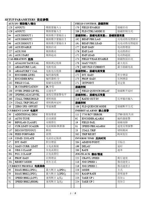
励磁控制
10
ZERO SPD. OFFSET
零速偏置
186
FLD QUENCH MODE
励磁断开方式
CURRENT LOOP电流环
INHIBIT ALARMS禁止报警30Βιβλιοθήκη ADDITIONAL DEM
附加要求
111
5730 RCV ERROR
5703接收失误
18
AUTO TUNE
自动调谐
92
程序停机时间
217
STOP LIMIT
停机极限
27
STOP TIME
停机时间
29
STOP ZERO SPEED
停机零速
SYSTEM系统
配置输入输出::模拟输入::ANIN 1(A2)
294
SPT SUM 1 DEST
设定值合计1目的
230
CALIBRATION
校准
442
TAPER
锥度
246
DESTINATION TAG
目的标记
CONFIGURE 5703配置输入输出::配置5703
231
MAX VALUE
最大值
135
DESTINATION TAG
目的标记
232
MIN VALUE
最小值
134
SOURCE TAG
源标记
配置输入输出::模拟输入::ANIN 2(A3)
CONFIGURE I/O配置输入输出
233
CALIBRATION
110
VALUE FOR FALSE
“虚”的值
241
MIN VALUE
最小值
109
Analog and Digital(模拟电子和数字电子)电子信息专业英语文章

Analog and Digital(模拟电子和数字电子)英文原稿:Analog and DigitalIdeal Operational Amplifiers and Practical Limitations In order to discuss the ideal parameters of operational amplifiers, we must firstdefine the terms, and then go on to describe what we regard as the ideal values forthose terms. At first sight, the specification sheet for an operational amplifier seems to list a large number of values, some in strange units, some interrelated, and often confusing to those unfamiliar with the subject. The approach to such a situation is to be methodical, and take the necessary time to read and understand each definition in the order that it is listed. Without a real appreciation of what each means, the designer is doomed to failure. The objective is to be able to design a circuit from the basis of the published data, and know that it will function as predicted when the prototype is constructed.1It is all too easy with linear circuits, which appear relatively simple when compared with today’s complex logic arrangements, to ignore detailed performance parameters which can drastically reduce the expected performance.Let us take a very simple but striking example. Consider a requirement for anamplifier having a voltage gain of 10 at 50 kHz driving into a 10 k load. A commonlow-cost, internally frequency-compensated op amp is chosen; it has the requiredbandwidth at a closed-loop gain of 10, and it would seem to meet the bill. The deviceis connected, and it is found to have the correct gain. But it will only produce a fewvolts output swing when the data clearly shows that the output should be capable ofdriving to within two or three volts of the supply rails. The designer has forgotten thatthe maximum output voltage swing is severely limited by frequency, and that themaximum low-frequency output swing becomes limited at about 10 kHz. Of course,the information is in fact on the data sheet, but its relevance has not been appreciated.This sort of problem occurs regularly for the inexperienced designer. So the moral isclear: always take the necessary time to write down the full operating requirementsbefore attempting a design. Attention to the detail of the performance specificationwill always be beneficial. It is suggested the following list of performance details beconsidered:1. Closed loop gain accuracy, stability with temperature, time and supply voltage2. Power supply requirements, source and load impedances, power dissipation3. Input error voltages and bias currents. Input and output resistance, drift withtime and temperature4. Frequency response, phase shift, output swing, transient response, slew rate,frequency stability, capacitive load driving, overload recovery5. Linearity, distortion and noise6. Input, output or supply protection required. Input voltage range,common-mode rejection7. External offset trimming requirementNot all of these terms will be relevant, but it is useful to remember that it is better to consider them initially rather than to be forced into retrospective modifications.All parameters are subject to wide variationsNever forget this fact. How many times has a circuit been designed using typical values, only to find that the circuit does not work because the device used is not typical? The above statement thus poses a tricky question: when should typical values and when should worst-case values be used in the design? This is where the judgment of the experienced designer must be brought to bear. Clearly, if certain performance requirements are mandatory, then worst-case values must be used. In many cases, however, the desirability of a certain defined performance will be a compromise between ease of implementation, degree of importance, and economic considerations. Do not over-specify or over-designIn the end, we are all controlled by cost, and it is really pointless taking a sledgehammer to crack a nut, Simplicity is of the essence since the low parts count implementation is invariably cheaper and more reliable.As an example of this judgment about worst-case design, consider a low-gain DC transducer amplifier required to amplify 10 mV from a voltage source to produce an output of .l V with an accuracy of ±1% over a temperature range of 0~70︒C. Notice that the specification calls for an accuracy of ±1%. This implies that the output should be 1 V ±10 mV from 0 ~ 70︒C. The first step is, of course, to consider our list above, and decide which of the many parameters are relevant. Two of the most important to this (very limited) specification are offset voltage drift and gain stability with temperature. We will assume that all initial errors are negligible (rarely the case in practice). The experienced designer would know that most op amps have a very large open-loop gain, usually very much greater than 10000. A closed-loop gain change of ±1% implies that the loop gain (as explained later) should change by less than ±100% for a closed-loop gain of 100. This is clearly so easily fulfilled that the designer knows immediately that he can use typical open-loop gain values in his calculations. However, offset voltage drift is another matter. Many op amp specifications include only typical values for offset voltage drift; this may well be in the order of 5 μV/︒C, with an unquoted maximum for any device of 30 μV/︒C. If by chance we use a device which has this worst-case drift, then the amplifier error could be 30×70=2100 μV=2.1 mV over temperature, which is a significant proportion of our total allowable error from all sources.Here is a case, then, where one can be confident that the typical value of open-loop gain can be used, but where the maximum value of drift may well cause significant errors. This sort of judgment is essential in careful design, and great care is required in interpreting manufacturers’ data. This consideration must be extended toall the details listed above apart from the fact that worst-case values are often not quoted. It is often found that values given are not 100% tested. Statistical testing is employed which, for example, guarantees that 90% of all devices fall within the range specified. It could be very inconvenient for the user who relies on the specified performance and then finds that he has several of the ‘other’ 10% actually plugged into his circuit.Data Registers and CountersData registerThe simplest type of register is a data register, which is used for the temporary storage of a “word” of data. In its simplest form, it consists of a set of N D flip-flops, all sharing a common clock. All of the digits in the N bit data word are connected to the data register by an N-line “data bus”. Figure 1.1 shows a 4 bit data register, implemented with four D flip-flops. The data register is said to be a synchronous device, because all the flip-flops change state at the same time.Shift registersAnother common form of register used in computers and in many other types of logic circuits is a shift register. It is simply a set of flip-flops (usually D latches or RS flip-flops) connected together so that the output of one becomes the input of the next, and so on in series. It is called a shift register because the data is shifted through the register by one bit position on each clock pulse. Figure 1.2 shows a 4 bit shift register, implemented with D flip-flops.On the leading edge of the first clock pulse, the signal on the DATA input is latched in the first flip-flop. On the leading edge of the next clock pulse, the contents of the first flip-flop is stored in the second flip-flop, and the signal which is present at the DATA input is stored in the first flip-flop, etc. Because the data is entered one bit at a time, this called a serial-in shift register. Since there is only one output, and data leaves the shift register one bit at a time, then it is also a serial out shift register. (Shift registers are named by their method of input and output; either serial or parallel.) Parallel input can be provided through the use of the preset and clear inputs to the flip-flop. The parallel loading of the flip-flop can be synchronous (i.e., occurs with the clock pulse) or asynchronous (independent of the clock pulse) depending on the design of the shift register. Parallel output can be obtained from the outputs of each flip-flop as shown in Figure 1.3.Communication between a computer and a peripheral device is usually done serially, while computation in the computer itself is usually performed with parallel logic circuitry. A shift register can be used to convert information from serial form to parallel form, and vice versa. Many different kinds of shift registers are available, depending upon the degree of sophistication required.Counters — weighted coding of binary numbersIn a sense, a shift register can be considered a counter based on the unary numbersystem. Unfortunately, a unary counter would require a flip-flop for each number in the counting range. A binary weighted counter, however, requires only flip-flops to count to N. A simple binary weighted counter can be made using T flip-flops. The flip-flops are attached to each other in a way so that the output of one acts as the clock for the next, and so on. In this case, the position of the flip-flop in the chain determines its weight; i.e., for a binary counter, the “power of two” it corresponds to.A 3-bit (modulo 8) binary counter could be configured with T flip-flops as shown in Figure 1.4. A timing diagram corresponding to this circuit is shown in Figure 1.5.Note that a set of lights attached to O0, O1, O2 would display the numbers of full clock pulses which had been completed, in binary (modulo 8), from the first pulse. As many T flip-flops as required could be combined to make a counter with a large number of digits.Note that in this counter, each flip-flops changes state on the falling edge of the pulse from the previous flip-flop. Therefore there will be a slight time delay, due to the propagation delay of the flip-flops between the time one flip-flop changes state and the time the next one changes state, i.e., the change of state ripples through the counter, and these counters are therefore called ripple counters. As in the case of a ripple carry adder, the propagation delay can become significant for large counters.It is possible to make, or buy in a single chip, counters which will count up, count down, and which can be preset to any desired number. Counters can also be constructed which count in BCD and base 12 or any other number base.A count down counter can be made by connecting the Q output to the clock input in the previous counter. By the use of preset and clear inputs, and by gating the output of each T flip- flop with another logic level using AND gates (say logic 0 for counting down, logic 1 for counting up), then a presetable up-down binary counter can be constructed. Figure 1.6 shows an up-down counter, without preset or clear.Synchronous countersThe counters shown previously have been “asynchronous counters”; so called because the flip-flops do not all change state at the same time, but change as a result of a previous output. The output of one flip-flop is the input to the next; the state changes consequently “ripple through” the flip-flops, requiring a time proportional to the length of the counter. It is possible to design synchronous counters, using JK flip-flops, where all flip-flops change state at the same time; i.e., the clock pulse is presented to each JK flip-flop at the same time. This can be easily done by nothing that, for a binary counter, any given digit changes its value (from 1 to 0 or from 0 to 1) whenever all the previous digits have a value of 1. A count down timer can be made by connecting the Q output to the J and K, through the AND gates. Preset and clear could also be provided, and the counter could be made “programmable” as in the previous case.The timing diagram is similar to that shown for the asynchronous (ripple) counters, except that the ripple time is now zero; all counters clock at the same time. It is common for synchronous counters to trigger on the positive edge of the clock,rather than the trailing edge.Nature of Phase LockThe phase detector compares the phase of a periodic input signal against the phase of the VCO. Output of PD is a measure of the phase difference between its two inputs. The difference voltage is then filtered by the loop filter and applied to the VCO. Control voltage on the VCO changes the frequency in a direction that reduces the phase difference between the input signal and the local oscillator.When the loop is locked, the control voltage is such that the frequency of the VCO is exactly equal to the average frequency of the input signal. For each cycle of input there is one, and only one, cycle of oscillator output. One obvious application of phase lock is in automatic frequency control (AFC). Perfect frequency control can be achieved by this method, whereas conventional AFC techniques necessarily entail some frequency error.To maintain the control voltage needed for lock it is generally necessary to have a nonzero output from the phase detector. Consequently, the loop operates with some phase error present. As a practical matter, however, this error tends to be small in a well-designed loop.A slightly different explanation may provide a better understanding of loop operation. Let us suppose that the incoming signal carries information in its phase or frequency; this signal is inevitably corrupted by additive noise. The task of a phase lock receiver is to reproduce the original signal while removing as much of the noise as possible.To reproduce the signal the receiver makes use of a local oscillator whose frequency is very close to that expected in the signal. Local oscillator and incoming signal waveforms are compared with one another by a phase detector whose error output indicates instantaneous phase difference. To suppress noise the error is averaged over some length of time, and the average is used to establish frequency of the oscillator.If the original signal is well behaved (stable in frequency), the local oscillator will need very little information to be able to track, and that information can be obtained by averaging for a long period of time, thereby eliminating noise that could be very large. The input to the loop is a noisy signal, whereas the output of the VCO is a cleaned-up version of the input. It is reasonable, therefore, to consider the loop as a kind of filter that passes signals and rejects noise.Two important characteristics of the filter are that the bandwidth can be very small and that the filter automatically tracks the signal frequency. These features, automatic tracking and narrow bandwidth, account for the major uses of phase lock receivers. Narrow bandwidth is capable of rejecting large amounts of noise; it is not at all unusual for a PLL to recover a signal deeply embedded in noise.History and applicationAn early description of phase lock was published by de Bellescize in 1932 and treated the synchronous reception of radio signals. Superheterodyne receivers hadcome into use during the 1920s, but there was a continual search for a simpler technique; one approach investigated was the synchronous, or homodyne, receiver. In essence, this receiver consists of nothing but a local oscillator, a mixer, and an audio amplifier. To operate, the oscillator must be adjusted to exactly the same frequency as the carrier of the incoming signal, which is then converted to an intermediate frequency of exactly 0 Hz. Output of the mixer contains demodulated information that is carried as sidebands by the signal. Interference will not be synchronous with the local oscillator, and therefore mixer output caused by an interfering signal is a beat-note that can be suppressed by audio filtering.Correct tuning of the local oscillator is essential to synchronous reception; any frequency error whatsoever will hopelessly garble the information. Furthermore, phase of the local oscillator must agree, within a fairly small fraction of a cycle, with the received carrier phase. In other words, the local oscillator must be phase locked to the incoming signal.For various reasons the simple synchronous receiver has never been used extensively. Present-day phase lock receivers almost invariably use the superheterodyne principle and tend to be highly complex. One of their most important applications is in the reception of the very weak signals from distant spacecraft. The first widespread use of phase lock was in the synchronization of horizontal and vertical scan in television receivers. The start of each line and the start of each interlaced half-frame of a television picture are signaled by a pulse transmitted with the video information. As a very crude approach to reconstructing a scan raster on the TV tube, these pulses can be stripped off and individually utilized to trigger a pair of single sweep generators.A slightly more sophisticated approach uses a pair of free-running relaxation oscillators to drive the sweep generators. In this way sweep is present even if synchronization is absent.Free-running frequencies of the oscillators are set slightly below the horizontal and vertical pulse rates, and the stripped pulses are used to trigger the oscillators prematurely and thus to synchronize them to the line and half-frame rates (half-frame because United States television interlaces the lines on alternate vertical scans).In the absence of noise this scheme can provide good synchronization and is entirely adequate. Unfortunately, noise is rarely absent, and any triggering circuit is particularly susceptible to it. As an extreme, triggered scan will completely fail at a signal-to-noise ratio that still provides a recognizable, though inferior, picture.Under less extreme conditions noise causes starting-time jitter and occasional misfiring far out of phase. Horizontal jitter reduces horizontal resolution and causes vertical lines to have a ragged appearance. Severe horizontal misfiring usually causes a narrow horizontal black streak to appear.Vertical jitter causes an apparent vertical movement of the picture. Also, the interlaced lines of successive half-frames would so move with respect to one another that further picture degradation would result.Noise fluctuation can be vastly reduced by phase locking the two oscillators to the stripped sync pulses. Instead of triggering on each pulse a phase-lock techniqueexamines the relative phase between each oscillator and many of its sync pulses and adjusts oscillator frequency so that the average phase discrepancy is small.Because it looks at many pulses, a phase lock synchronizer is not confused by occasional large noise pulses that disrupt a triggered synchronizer. The flywheel synchronizers in present day TV receivers are really phase-locked loops. The name “flywheel” is used because the circuit is able to coast through periods of increased noise or weak signal. Substantial improvement in synchronizing performance is obtained by phase-lock.In a color television receiver, the color burst is synchronized by a phase-lock loop.Space flight requirements inspired intensive application of phase lock methods. Space use of phase lock began with the launching of the first American artificial satellites. These vehicles carried low-power (10 mW) CW transmitters; received signals were correspondingly weak. Because of Doppler shift and drift of the transmitting oscillator, there was considerable uncertainty about the exact frequency of the received signal. At the 108 MHz frequency originally used, the Doppler shift could range over a ±3 kHz interval.With an ordinary, fixed-tuned receiver, bandwidth would therefore have to be at least 6 kHz, if not more. However, the signal itself occupies a very narrow spectrum and can be contained in something like a 6 Hz bandwidth.Noise power in the receiver is directly proportional to bandwidth. Therefore, if conventional techniques were used, a noise penalty of 1000 times (30 dB) would have to be accepted. The numbers have become even more spectacular as technology has progressed; transmission frequencies have moved up to S-band, making the Doppler range some ±75 kHz, whereas receiver bandwidths as small as 3 Hz have been achieved. The penalty for conventional techniques would thus be about 47 dB. Such penalties are intolerable and that is why narrowband, phase-locked, tracking receivers are used.Noise can be rejected by a narrowband filter, but if the filter is fixed the signal almost never will be within the pass-band. For a narrow filter to be usable it must be capable of tracking the signal. A phase-locked loop is capable of providing both the narrow bandwidth and the tracking that are needed. Moreover, extremely narrow bandwidths can be conveniently obtained (3 to 1000 Hz are typical for space applications); if necessary, bandwidth is easily changed.For a Doppler signal the information needed to determine vehicle velocity is the Doppler shift. A phase-lock receiver is well adapted to Doppler recovery, for it has no frequency error when locked.Other applicationsThe following applications, further discussed elsewhere in the book, represent some of the current uses of phase-lock.1. One method of tracking moving vehicles involves transmitting a coherentsignal to the vehicle, offsetting the signal frequency, and re-transmitting back to the ground. The coherent transponder in the vehicle must operate so that the input and output frequencies are exactly related in the ratio m/n, where m and nare integers. Phase-lock techniques are often used to establish coherence.2. A phase-locked loop can be used as a frequency demodulator, in which it hassuperior performance to a conventional discriminator.3. Noisy oscillators can be enclosed in a loop and locked to a clean signal. If theloop has a wide bandwidth, the oscillator tracks out its own noise and its output is greatly cleaned up.4. Frequency multipliers and dividers can be built by using PLLs.5. Synchronization of digital transmission is typically obtained by phase-lockmethods.6. Frequency synthesizers are conveniently built by phase-lock loops.中文翻译:模拟电子和数字电子理想运算放大器和实际限制为了讨论运算放大器的理想参数,我们必须首先定义一些指标项,然后对这些指标项讲述我们所认为的理想值。
Analog Devices IC (ADE) 产品系列简介说明书

Energy Measurement ProductsADE Product Family OverviewThe Analog Devices IC (ADE) family combines industry-leading data conversion technology with a fixed function digital signal processor (DSP) to perform the calculations essential to an electronic energy meter. The portfolio includes single-phase products and polyphase products for stepper motor and LCD display meter designs, with five critical measurements available: watt, V rms, I rms, VA, and VAR.With 175 million units deployed in the field, ADI has added to the portfolio the ADE71xx and ADE75xx product families that simplify energy meter design by providing all the features needed for an accurate, reliable, and fully functional energymeter with LCD display in a single IC.ADE Product Family • High accuracy exceeds IEC and ANSI standards • Proprietary 16-bit ADCs and DSP provide high accuracy over large variations in current, environmental conditions, and time • Reliability proven with over 175 million units deployed in the field• On-chip reference with low temperature drift (20 ppm to 30 ppm typ)• On-chip power supply monitoring• On-chip creep protection (no-load threshold)• Single 5 V supply • Low power consumption • Instantaneous active power output for calibration or interface to an MCU • Miswiring or reverse power indication• Tamper detection optionsADE Pulsed Output Products or Stepper Motor Display Meters • Exceeds IEC 61036/62053-21, IEC 60687/62053-22, ANSI C12.16, and ANSI C12.20• Active energy measurement with less than 0.1% error over a dynamic range of 500 to 1 at 25°C• Power consumption as low as 15 mW (typ) for single-phase products and 30 mW (typ) for polyphase products• Built-in current channelamplifier allows the use of low resistance, low cost shunts • Active energy, low frequency outputs directly driveelectromechanical counters • Single 5 V supplyADE Serial Interface Products for LCD Meters• Exceeds IEC 61036/62053-21, IEC 60687/62053-23 (for multifunction products), ANSI C12.16, and ANSI C12.20• Active energy measurement with less than 0.1% error over a dynamic range of 1000 to 1 at 25°C• Active energy and sampled waveform data• Multifunction products provide VAR, VA, V rms, and I rms • User-programmable power quality monitoring features • Digital calibration for power, phase, and offset• Serial peripheral interface (SPI) with interrupt request pin (IRQ)• Single 5 V supplyIntegrated Products for LCD Meters• Exceeds IEC 61036/62053-21, IEC 60687/62053-23 (for multifunction products), ANSI C12.16, and ANSI C12.20• Single chip solution integrates ADE measurement core for watts, VAR, VA, V rms, and I rms• 8052 MCU core with flash memory• 104-segment LCD driver with contrast control for low/high temperature visibility • Low power RTC (1.5 μA typ) with digital compensation for temperature performance • Power fail and batterymanagement with no external components• Reference with low temperature drift (5 ppm/°C typ)• Noninvasive in-circuitemulation/energymeterValue of ADE Products1. Proven TechnologyAnalog Devices is the market leader in sales of energy metering ICs with over 175 million meters deployed worldwide with ADE products.• Quality: Strict quality and test standards applied to ADE products throughout design and manufacturing stages ensure low meter production failure rate and uniform part-to-part characteristics.• Reliability: Accelerated life expectancy tests on ADE products, representing more than 60 years of field usage, reduce probability of meter failure due to IC failure.• Performance: Proprietary Σ-∆ ADCs provide excellent performance with an error of less than 0.1% over an extended current dynamic range.2. Ease of DesignAnalog Devices ADE solutions aim to simplify energy meter design, reduce system cost, and reduce time to market with:• Integration of ADCs and fixed function DSP on a single chip leading to a single IC energy meter• Integration of ADCs and fixed function DSP on a single chip reduces processing requirements, enabling the use of a lower cost MCU • Embedded essential energy calculations to ensure harmonic content is included (up to 233rd harmonics for watt-hour measurement)• Direct and flexible sensor interface without external gain amplifiers• Unparalleled design support including detailed data sheets, reference designs, application notes, evaluation tools, and technical support • Integrated MCU core, and all necessary peripherals, with field proven metering front end • Greater system control with minimized current consumption in battery mode3. Innovation and ChoiceAnalog Devices is committed to continuing its investment in the ADE product family and to enabling very competitive system costs while maintaining a high level of innovation.• 16 patents granted or pending on innovative energy measurement technology• Many energy measurement products currently available for single-phase and polyphase energy meters with more to come4. Quality• Samples from production lots constantly drawn for rigorous qualifications• ADI’s product analysis group continually addresses customer concerns and feedback on the quality of our products • Constant monitoring of electrical ppm failure rate of finished products• Electrical ppm failure rate is largely comprised of marginal parametric rejects that are fully functional but are most likely to experience failure in the field•ADI products have a consistently low ppm failure rate that reflects the stability and high quality of the manufacturing process• TIME DEPENDENT DIELECTRIC BREAKDOWN • ELECTROMIGRATION• HOT CARRIER INJECTION• THERMAL SHOCK SEQUENCE• TEMPERATURE CYCLING SEQUENCE• ELECTRICAL ENDURANCE—HTOL AND LTOL • EARLY LIFE FAILURE CHARACTERIZATION • HIGH TEMPERATURE STORAGE • MOISTURE ENDURANCE TEST • DIE SHEAR TEST• FABRICATION AND ASSEMBLY QUALIFICATION • ELECTRICAL STATIC DISCHARGE (ESD)• LATCH UPPRODUCTION QUALITY CONTROL SUPPLEMENTAL QUALIFICATIONS APPLICATION SPECIFIC QUALIFICATIONEND PRODUCT QUALIFICATIONFABRICATION QUALIFICATIONASSEMBLY QUALIFICATIONANALOG DEVICESSTANDARD QUALIFICATIONS LIST OF QUALIFICATIONSPASSEDPASSEDCUSTOMER FEEDBACK• BOND STRENGTH • BURN-IN SEQUENCE• CONSTANT ACCELERATION • HERMETICITY• HIGH TEMPERATURE STORAGE • INTERNAL WATER VAPOR TEST • LEAD FATIGUE • LID TORQUE• MARKING PERMANENCY • MECHANICAL SHOCK• MOISTURE SENSITIVITY CHARACTERIZATION• MOISTURE ENDURANCE SEQUENCE AND AUTOCLAVE • RESISTANCE TO SOLDERING HEAT • SOLDERABILITY• THERMAL IMPEDANCE• VIBRATION, VARIABLE FREQUENCY • X-RAY INSPECTIONReliabilityAnalog Devices conducted a high temperature operating lifetest (HTOL) to simulate aging of ADE products in the field.Method—ICs subjected to 150°C for 3000 hours:• With acceleration factor of 179×, the life expectancy correlates to 60 years at operating temperature of 60°C.• Four main parameters monitored: reference voltage, gain error, current, and voltage channel offset.Results—parameter distribution over time shows:• Negligible parameter distribution shifts.• Parameters maintain data sheet specifications.• Zero failures.Conclusions from HTOL test:• If other components in electronic meter have the same life expectancy, meter replacement is only needed every 60 years.• Proven stability and accuracy of digital energy measurement.Meter manufacturers must carefully select components to ensure that the overall reliability of electronic energy meter is maximized.10,000125OPERATING TEMPERATURE (°C)A C C E L E R A T I O N F A C T O R10001001010,0001L I F E T I M E (Y e a r s )100010010303540455055606570758085PerformanceThe unsurpassed accuracy of power calculation over a very wide dynamic range, harmonics, and stability over time are the primary reasons why ADE ICs are preferred by many meter manufacturers around the world. The plot to the right highlights the typical performance of ADE ICs over a dynamic range of 1000:1 and temperature range of –40°C to +85°C. Even at a low power factor (PF = 0.5), the ICs maintain their high accuracy.0.4–0.4AMPSE R R O R (%)0.30.20.10–0.1–0.2–0.3Reliability Lifetime PredictionsTypical Performance for ADE ICs"%$"%$"%$&/&3(:.&"463&.&/5%41*/5&3/"- 7 QQN $4*/(-&$:$-& .$66"3541* *$8%53".108&3 4611-:$0/530-108&3 4611-:.0/*503*/(-%0103"%$*/5&3/"-3&4&5"%$5&.1&3"563&4&/403*/5&3/"- 147 ."9$)"3(& 16.1%"$-$% %3*7&3 4&(.&/541--*/5&3/"-$-0$,35$'-"4).&.03:"%& YY "%& YYSelection GuideADE71xx/ADE75xx: Energy Measurement Computing EngineThe ADE71xx/ADE75xx family builds on Analog Devices’ 10 years of experience in energy measurement to provide the best analog-to-digital converters combined with the advanced digital signal processing required to build an accurate, robust, and fully featured energy meter with LCD display.Energy Measurement Key Features:• Exceeds IEC 61036/62053-21,IEC 60687/62053-22, IEC 61268/62053-23, ANSI C12.16, and ANSI C12.20• 4-quadrant power and energy measurement for:• Active, reactive, and apparent• Tampering protection• 2 current inputs for line and neutral • Tampering algorithms integrated • Special energy accumulation modes• Shunt, current transformer, and di/dt current sensor connectivity enabled• 2 high precision pulse outputs for calibration • Power line quality: SAG, period/frequency, peak, zero-crossing• Large phase calibration (5° @ 50 Hz)• Wide measurement frequency bandwidth (14 kHz) for harmonic measurementADE71xx/ADE75xx: LCD DriverThe ADE71xx/ADE75xx family has a unique LCD driver capable of maintainingmaximum contrast on the LCD independently of the power supply level using charge-pump circuitry. This technology combined with the on-chip temperature measurement enables the lowest power operation and maximum readability of the energy meter LCD display.LCD Driver Key Features:• 104-segment LCD driver• Adjustable LCD voltage (5 V max) independent of the power supply (2.7 V min)• LCD freeze and hardware blink functions for low power operation in battery mode • Low offset to minimize LCD fluid biasingRTC Key Features:•1.5 μA current consumption•Low voltage operation: 2.4 V•2 ppm/LSB digital frequency adjustment for calibration and temperature compensation •Alarm and midnight interruptsADE71xx/ADE75xx: Real-Time ClockThe ADE71xx/ADE75xx family provides a low power RTC with nominal and temperature dependent crystal frequency compensation capabilities enabling low drift and high accuracy timekeeping. The RTC functionality is also maintained at low power supply (2.4 V) and over all power supply connections, extending the operating life of the energy meter in battery mode.ADE71xx/ADE75xx: Battery ManagementThe ADE71xx/ADE75xx family has unique battery management features enabling low power consumption in battery mode and optimal power supply management when line voltage is lost.Battery Management Key Features:•No external circuitry for battery switching•Power supply switching based on absolute level•Early warning of power supply collapse with SAG and preregulated power supply monitoring•Internal power supply always valid by hardware controlled switchover to batteryKey Features Maintained in Battery Mode:•Real-time clock for timekeeping•LCD display•Temperature measurement•Meter wake-up events such as RTC alarms, I/O, UART activitiesADE Development ToolsThe ADE71xx and ADE75xx family of products share a common set of tools designedto minimize design time while improving the part understanding. These tools arecomprised of:• Energy meter reference design• 1-pin emulator with isolated USB interface• Isolated USB to UART debugger interface• Downloader software• Evaluation software• Integrated development environment from well-known vendor• Firmware libraries for common and part specific functionsThe energy meter reference design integrates the main functions of an LCD meter withIR port and RS-485 communication, battery backup, two current sensors, antitamperinterface, and EEPROM interface while using the features of the ADE71xx and ADE75xxseries such as battery management, antitamper detection, temperature compensatedreal-time clock, and LCD driver contrast.The reference design is accompanied by code libraries and an example of systemintegration code allowing easy evaluation and further development of solution.Isolated USB communication boards for debugging and emulation provide a safesolution for code development when the meter is connected to the line.The ADE71xx and ADE75xx series can be used with integrated developmentenvironments (IDE) from open market vendors to simulate, compile, debug, anddownload assembly or C code. A free of charge IDE with unlimited assembly codecapability and 4 kB limited C code capability is included in the evaluation kit. Inaddition, the part can be evaluated with a UART interface and a PC by using theversatile evaluation tools and downloader.Single-Phase Energy Metering ICs with Integrated OscillatorThe AD71056, ADE7768, and ADE7769 are single-phase ICs that provide watt-hour information using pulse outputs that directly drive a stepper motor counter.The AD71056, ADE7768, and ADE7769 are pin-reduced versions of the ADE7755, with the enhancement of an on-chip, precisionoscillator circuit that serves as the clock source for the IC. The direct interface to low resistance, low cost shunt resistors also helps to lower the cost of a meter built with AD71056, ADE7768, or ADE7769.These products are pin compatible. The AD71056 and ADE7769 accumulate bidirectional power information, and the ADE7768accumulates power only in the positive direction providing flexibility for various billing schemes. The ADE7769 indicates when the power is below the no-load threshold by holding the calibration frequencypin high. This is useful to indicate a tampering or miswired condition.Single-Phase Energy Metering ICs with Antitamper FeaturesThe ADE7761B detects two common tampering conditions: “fault” condition (when loads are grounded to earth instead of connected to neutral wire or when the meter is bypassed with external wires) and “missing neutral” condition (when the voltage input and return current are missing). The ADE7761B incorporates a novel tampering detection scheme which indicates the fault or missing neutral conditions and allows the meter to continue accurate billing by continuous monitoring of the phase and neutral (return) currents. A fault is indicated when these currents differ by more than 6.25%, and billing continues using the larger of the two currents. The missing neutral condition is detected when no voltage input is present, and billing is continued based on the active current signal. The ADE7761B also includes a power-supply monitoring circuit which ensures that the voltage and current channels are matched,eliminating creep effects in the meter.Polyphase Energy Metering ICs with Pulse OutputThe ADE7752A, ADE7752B, and ADE7762 are polyphase ICs that provide watt-hour information using pulse outputs that can directly drive a stepper motor counter. Compatible with a wide range of 3-phase grid configurations, including 3-wire and 4-wire delta and wye distributions, each of these products can be used for 3-phase commercial and industrial revenue meters or submeters, 3-phase motors or generators, industrial control, and utility automation. The ADE7762 and ADE7752B are optimized for 3-phase, 3-wire applica-tions with no-load threshold and REVP indication based on the sum of the phases.To ensure that energy is billed properly under miswiring or tamper-ing conditions, any of the ICs can be set to accumulate based on the sum of the absolute value in each phase. The active power accumu-lation is signed by default.The ADE7762 has four additional logic output pins. These four pins drive six LEDs for prioritized indication of phase dropout and phasesequence error as well as reverse polarity per phase.ADE7752A and ADE7752B are pin compatible with the legacy ADE7752 and have up to a 50% power consumption reduction from ADE7752. The four additional pins of ADE7762 are located at the top of the package so that the same PCB may be used with an ADE7752A-, ADE7752B-, or ADE7762-based meter.10Single-Phase Energy Metering ICs with Serial InterfaceADI has a range of product offerings for single-phase energy measurement solutions requiring serial interface. The ADE7756 measures active energy and allows digital calibration of phase, offset, and gain through a serial port interface. The ADE7759 has a built-in digital integrator for direct interface with a di/dt sensor such as a Rogowski coil and includes the capability to interface with low resistance shunts and traditional current transformers. The ADE7753 provides active, apparent, and reactive energy measurements, and incorporates a built-in digital integrator to allow direct interface with a Rogowski coil sensor in addition to a low resistance shunt or CT. The ADE7763 provides the same functionality as the ADE7753 but without reactive energy measurement. All four of these ADE single-phase energy metering ICs with SPI are pin compatible for ease of design migration.11Polyphase Energy Metering ICs with Serial InterfaceADI has a selection of product offerings for3-phase energy measurement solutions requiring serial interface. The ADE7758 features second-order sigma-delta ADCs, and is designed formidrange 3-phase energy meters. For each phase, the chip measures active, reactive, and apparent energy, as well as rms voltage and rms current. These measurements are accessed via an SPI that allows a fully automated digital calibration. The ADE7758 interfaces with a variety of sensors, including current transformers and di/dt current sensors, such as Rogowski coils. Additionally, the ADE7758 provides a programmable frequency pulse output for both active and apparent orreactive power.Analog Devices, Inc.Worldwide Headquarters Analog Devices, Inc. One Technology Way P .O. Box 9106Norwood, MA 02062-9106 U.S.A.Tel: 781.329.4700 (800.262.5643, U.S.A. only)Fax: 781.461.3113Analog Devices, Inc. Europe Headquarters Analog Devices, Inc.Wilhelm-Wagenfeld-Str. 6 80807 Munich GermanyTel: 49.89.76903.0 Fax: 49.89.76903.157Analog Devices, Inc. Japan Headquarters Analog Devices, KK New Pier Takeshiba South Tower Building 1-16-1 Kaigan, Minato-ku, Tokyo, 105-6891 JapanTel: 813.5402.8200 Fax: 813.5402.1064Analog Devices, Inc. Southeast Asia Headquarters Analog Devices22/F One Corporate Avenue 222 Hu Bin Road Shanghai, 200021 ChinaTel: 86.21.5150.3000 Fax: 86.21.5150.3222©2007 Analog Devices, Inc. All rights reserved. Trademarks and registered trademarks are the property of their respective owners.Printed in the U.S.A. BR04915-5-8/07(A)/energymeter。
ADRV9026四通道宽带RF接收器平台商品介绍说明书

VISIT ADRV9026Quad-Channel, Wideband RF Transceiver Platform200 MHz Bandwidth Integrated Radio Transceiver SolutionApplications►Macro base stations ►Massive MIMO►Small cell designs1See page 3 for future enhancements in the ADRV902x family roadmapSmallest Size, Lowest Power Transceiver Solution for Base Transceiver Stations (BTS )►Smallest size reduces footprint and enhances form factor flexibility►50% power consumption reduction over previous generation ADRV9009 for increased radio density►Enables ORAN small cell designs with lowest system power and costHighly Integrated, High Performance Software-Defined Radio►2× integration over ADRV9009►Supports up to 200 MHz bandwidth and covers all bands from 650 MHz to 6 GHz 1Common Platform Design for 3G/4G/5G Reduces Complexity, Development Costs, and Time to Market►Single-chip FDD/TDD solution simplifies hardware and software development ►Common API across multiple applications►Reduces product development cycles for band and power variants►Enables modular architecture for scalable radio solutionsADRV9026 Quad-Channel, Wideband RF Transceiver Platform RF SynthRF Synth ORX1/ORX2TX 1TX 2RX10°90°RX2RX3+RX3–RX4+RX4–RX1+RX1–RX2+RX2–TX3+TX3–TX4+TX4–TX1+TX1–TX2+TX2–ORX3+ORX3–ORX4+ORX4–ORX2+ORX2–ORX1+RF SynthLO 1LO 2GPIO AuxADC AuxDACGPINT1JESD204B/C Serial InterfaceClock GenerationandSynchronizationDEVCLK±SYSREF±LO 2LO 1LO 2LO 1RX3, RX4, TX3, TX4, ORX 3/ORX4RX1, RX2, TX1, TX2, ORX 1/ORX2pFIR,LO Leakage,QEC, Tuning,InterpolationGPIO_ANA_n AUXADC_nSPI_CLKSPI_EN SPI_DO SPI_DIORXn_EN TXn_EN ORXn_EN VDDA_1P8VDDA_1P3VDDA_1P0VDIG_1P0EXT_LO1±EXT_LO2±PWR MGMTGPINT2RESET TESTSERDOUTA±SYNCIN1±SYNCIN2±SYNCIN3±SERDINA±SERDINB±SERDINC±SERDIND±LO 3LO 3SYNCOUT1±SYNCOUT2±8419VIF444SERDOUTB±SERDOUTC±SERDOUTD±MicroprocessorADCADCDACDACADCADCDecimation,pFIR,DC Offset,QEC,Tuning,OverloadDecimation,pFIR, AGC,DC Offset,QECTuning RSSI,OverloadControl InterfaceSPI Port0°90°0°90°2ADRV9026 Quad-Channel, Wideband RF Transceiver Platform3Visit ADRV9026 Overview►Four differential transmitters ►Four differential receivers►Two observation receivers with two inputs each ►Center frequency: 650 MHz to 6000 MHz ►Maximum receiver bandwidth: 200 MHz ►Maximum transmitter bandwidth: 200 MHz►Maximum transmitter synthesis bandwidth: 450 MHz►Maximum observation receiver bandwidth: 450 MHz►Fully integrated independent fractional-N radio frequency synthesizers ►Fully integrated clock synthesizer►Multichip phase synchronization for all local oscillators and baseband clocks ►Support of TDD/FDD 3G/4G/5G applications►16 Gbps JESD204B/C digital interfaceSee roadmap below for future enhancementsADRV9026 Family RoadmapEnhanced features and functions will be added to the ADRV9026 over time, including:►25 Gbps SERDES support►Extending LO frequency range down to 75 MHz►Support for an external LO►Filter Wizard to generate custom profilesAn enhanced version from the ADRV902x family will be released in 2020 with integrated DPD and CFR, reducing FPGA requirements, as well as lowering total system power and cost.RadioVerse Ecosystem and PartnershipsRadioVerse ® is a design and technology ecosystem for advanced radio design and development. We offer market-leading integrated transceiver technology, software tools, evaluation and prototyping platforms, a range of reference designs, and radio solutions. RadioVerse is building up a global partnership network to provide customers all levels of design support. ADRV9026’s partner network and reference design ecosystem will be launched on /radioverse in 2020.Evaluation SystemThe evaluation system comprises an FPGA carrier board ADS9-V2EBZ and a radio daughtercard, coming with two frequency bands of matching: –HB for 2.8 GHz to 6 GHz and –MB for 650 MHz to 2.8 GHz. Compatible evaluation software is provided for download, including API library, Windows GUI, and a binary image for FPGA configuration.Radio CardsCarrier BoardsSoftware and DriverE v a l u a t i o n S y s t e m►ADRV902X-HB/PCBZ (for 2.8 GHz to 6 GHz )►ADRV902X-MB/PCBZ (for 650 MHz to 2.8 GHz )►ADS9-V2EBZ(FPGA motherboard with Xilinx ® UltraScale+™)►Operating system-agnostic API source in ANSI C►Windows GUI for transceiver configuration and data capture►Binary image for FPGA configurationFor regional headquarters, sales, and distributors orto contact customer service and technical support, visit /contact.Ask our ADI technology experts tough questions, browse FAQs, or join a conversation at the EngineerZone Online Support Community. Visit .©2019 Analog Devices, Inc. All rights reserved. Trademarks and registered trademarks are the property of their respective owners.PH21775-11/19(A)VISIT 。