lm1117 芯片中文资料
lm1117使用说明

概述LM1117是一个低压差电压调节器系列。
其压差在1.2V输出,负载电流为800mA时为1.2V。
它与国家半导体的工业标准器件LM317有相同的管脚排列。
LM1117有可调电压的版本,通过2个外部电阻可实现1.25~13.8V输出电压范围。
另外还有5个固定电压输出(1.8V、2.5V、2.85V、3.3V和5V)的型号。
LM1117提供电流限制和热保护。
电路包含1个齐纳调节的带隙参考电压以确保输出电压的精度在±1%以内。
LM1117系列具有LLP、TO-263、SOT-223、TO-220和TO-252 D-PAK封装。
输出端需要一个至少10uF的钽电容来改善瞬态响应和稳定性。
替换型号X1117是IC网络超市自主的品牌,可以很好的替换LM1117。
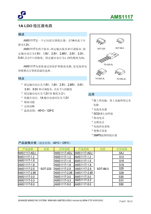
X1117是一款正电压输出的低压降三端线性稳压电路,在1A输出电流下的压降为1.2V。
分为两个版本,固定电压输出版本和可调电压输出版本。
固定输出电压1.5V、1.8V、2.5V、3.3V、5.0V和可调版本的电压精度为1%;固定电压为1.2V的产品输出电压精度为2%。
内部集成过热保护和限流电路,适用于各类电子产品。
A1117是台湾亿光研发生产的高效率低压降三端线性稳压器,A1117提供电流限制和热保护,以确保芯片和功率稳定性系统。
而在芯片上保证输出电压精度在±2%。
同时也提供了固定电压输出版本和可调电压输出版本,可调版本能输出从1.25V到13.8V。
特性提供1.8V、2.5V、2.85V、3.3V、5V和可调电压的型号节省空间的SOT-223和LLP封装电流限制和热保护功能输出电流可达800mA线性调整率:0.2% (Max)负载调整率:0.4% (Max).. 温度范围-LM1117:0℃~125℃-LM1117I:-40℃~125℃应用2.85V模块可用于SCSI-2有源终端开关DC/DC转换器的主调压器高效线性调整器电池充电器电池供电装置典型应用电路图。
MEMORY存储芯片LM1117IMPX-ADJ中文规格书
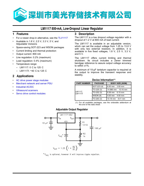
3 Description
The LM1117 is a low dropout voltage regulator with a dropout of 1.2 V at 800 mA of load current.
The LM1117 is available in an adjustable version, which can set the output voltage from 1.25 to 13.8 V with only two external resistors. In addition, it is available in five fixed voltages, 1.8 V, 2.5 V, 3.3 V, and 5 V.
(2) The maximum power dissipation is a function of TJ(max) , RθJA, and TA. The maximum allowable power dissipation at any ambient temperature is PD = (TJ(max)–TA)/RθJA. All numbers apply for packages soldered directly into a PCB.
A minimum of 10-µF tantalum capacitor is required at the output to improve the transient response and stability.
Device Information(1)
PART NUMBER PACKAGE
7.3 Recommended Operating Conditions
over operating free-air temperature range (unless otherwise noted)
LM1117-1.8 中文资料
1.176 1.2 1.224 V 1.152 1.2 1.248
1.485 1.500 1.515 V 1.470 1.500 1.530
VOUT AMS1117-1.8,
共10页 第4页
管脚排列图
AMS1117
AMS1117
AMS1117
AMS1117
AMS1117
AMS1117
管脚描述
管脚号 1 2 3
管脚名称 GND/ADJ
VOUT VIN
I/O
--/O 地/ADJ。
O
输出电压。
I
输入工作电压。
功能
ADVANCED MONOLITHIC SYSTEMS (translate by BONA 0755-82800289)
2.940 3.000 3.060
AMS1117-3.3, IOUT=10mA, VIN=5V,TJ=25°C , 0≤IOUT≤1A, 4.75V≤VIN≤10V
3.267 3.300 3.333 V 3.235 3.300 3.365
AMS1117-5.0,
IOUT=10mA, VIN=7V, TJ=25°C , 4.950 5.000 5.05 V
内部框图
ADVANCED MONOLITHIC SYSTEMS (translate by BONA 0755-82800289)
共10页 第2页
AMS1117
极限参数
参数 输入工作电压 引脚温度 (焊接5秒) 工作结温范围 储存温度 功耗 ESD能力 (最小值)
LM1117-2.5 中文资料

符号 VIN TLead TJ TSTG PD ESD
范围
20 260 150 -65 ~ +150 内部限制 (注1) 2000
单位 V °C °C °C
mW V
注1:最大允许功耗是最大工作结温TJ (max),结对空热阻θJA 和环境温度Tamb的函数。最大允许 功耗在给定的环境温度下, PD (max) = (TJ (max) - Tamb)/θJA,超过最大允许功耗会导致芯片 温度过高,调整器因此会进入到过热切断状态。不同封装类型的结对空热阻θJA 是不同的, 由封装技术决定。
ADJ R1
R2 VOUT=VREF x (1+R2/R1)+IADJ x R2
VOUT 22 F
图 2. 典型可调输出电压 注:以上线路及参数仅供参考,实际的应用电路请在充分的实测基础上设定参数。
111111111111111111111111111111111111111111111111111111 ADVANCED MONOLITHIC SYSTEMS (translate by BONA 0755-82800289)
VREF IOUT=10mA, VIN-VOUT=2V, TJ=25°C 1.238 1.250 1.262 V 10mA≤IOUT≤1A, 1.4V≤VIN-VOUT≤10V 1.225 1.250 1.270
AMS1117-1.2,
IOUT=10mΑ, VIN=3.2V ,TJ=25°C 10mA≤IOUT≤1A, 3.0V≤VIN≤10V
产品名称
AMS1117-ADJ AMS1117-1.2 AMS1117-1.5 AMS1117-1.8 AMS1117-2.5 AMS1117-2.85 AMS1117-3.0 AMS1117-3.3 AMS1117-5.0 AMS1117-ADJ AMS1117-1.2 AMS1117-1.5 AMS1117-1.8 AMS1117-2.5
LM1117_资料_new

(VIN - VOUT) ≤ 12V 时,该稳压器可保证正常工作。
应用注意点
LM1117 系列(可调整的和稳压的)应用简单但应防止短路和过热。 热保护电路在温 度超过165°C 时自动切断。引脚兼容带有老式三端调整器,这样在低电压偏差下提供了有 利的条件——精确了公差参数和提高了温度稳定性。
稳定性
LM1117 系列内部电路设计要求用一个输出电容器作为频率补偿。这个附加在输出部 分的22µF 的钽电容保证了所有运行条件的稳定性。当在这个调节器的旁路附加一个电容来 提高纹波抑制比时,它要求输出电容增大。22µF的钽电容代替了调整端的所有旁路,没有 这个旁路调整端要求更小的电容才能达到相同的效果。负载电流较大时为了得到好的瞬时特 性时,在许多的调整器里都是把电容定为100µf。其实可以进一步加大电容来提高稳定性和 纹波抑制比。
电池动力仪器
订购须知
封装类型
TO-252 LM1117T-ADJ LM1117T-1.5 LM1117T-1.8 LM1117T-2.5 LM1117T-2.85 LM1117T-3.3 LM1117T5.0
SOT-223 LM1117-ADJ LM1117-1.5 LM1117-1.8 LM1117-2.5 LM1117-2.85 LM1117-3.3 LM1117-5.0
10mA≤ IOUT ≤ 1A,
1.5V≤ (VIN - VOUT) ≤ 12V
T A =125°C, 1000Hrs
3
最小
标准
0.1 0.2 3 6 3 6 3 6 3 6 3 7 5 10
最大
0.3 0.4 10 20 10 20 12 20 12 20 15 25 20 35
单位
% % mV mV mV mV mV mV mV mV mV mV mV mV
LM1117_中文PDF资料
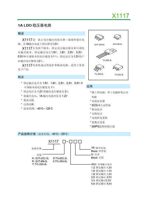
1A LDO稳压器电路概述是一款正电压输出的低压降三端线性稳压电路,在1A输出电流下的压降为1.2V。
分为两个版本,固定电压输出版本和可调电压输出版本。
固定输出电压1.5V、1.8V、2.5V、3.3V、5.0V和可调版本的电压精度为1%;固定电压为1.2V的产品输出电压精度为2%。
内部集成过热保护和限流电路,适用于各类电子产品。
特点*固定输出电压为1.5V、1.8V、2.5V、3.3V、5.0V和可调版本的电压精度为1%*固定电压为1.2V的输出电压精度为2%*低漏失电压:1A输出电流时仅为 1.2V*限流功能*过热切断*温度范围:-40°C~ 125°C应用*膝上型电脑,掌上电脑和笔记本电脑*电池充电器* SCSI-II主动终端*移动电话*无绳电话*电池供电系统*便携式设备* SMPS波斯特稳压器产品规格分类(温度范围:-40°C~ 125°C)X1117X1117X1117X1117X1117换页UX产品名称封装打印名称材料包装X 1117H - ADJ无铅编带X 1117H- 1.8TRX 1117H - 1.8编带X 1117H- 3.3TRX 1117H - 3.3编带SOT-223-3LX 1117H- ADJTR编带编带编带无铅无铅X 1117H- ADJTRX 1117H- 1.8TRX 1117H- 3.3TRX 1117H - ADJX 1117H - 3.3X 1117H - 1.8无卤无卤无卤内部框图3带隙限流TSD21AVOUTADJ/GNDVIN固定版本:F1和F2连接A断开可调版本: A连接, F1和 F2断开F1F2X1117换页极限参数参数符号范围单位输入工作电压引脚温度 (焊接5秒)TLead260°C工作结温范围TJ150°C储存温度TSTG-65 ~ +150°C功耗PD内部限制 (注1)mWESD能力 (最小值)ESD2000V注1:最大允许功耗是最大工作结温TJ (max),结对空热阻θJA和环境温度Tamb的函数。
LM1117_3.3中文PDF资料
范围 20 260 150
-65 ~ +150 内部限制 (注1)
2000
单位 V °C °C °C
mW V
注1:最大允许功耗是最大工作结温TJ (max),结对空热阻θJA 和环境温度Tamb的函数。最大允许 功耗在给定的环境温度下, PD (max) = (TJ (max) - Tamb)/θJA,超过最大允许功耗会导致芯片 温度过高,调整器因此会进入到过热切断状态。不同封装类型的结对空热阻θJA 是不同的, 由封装技术决定。
VIN 3
带隙 F1 A
TSD
限流
VOUT 2
固定版本: F1和F2 连接, A断开
F2
可调版本: A 连接, F1 和 F2 断开
1
ADJ/GND
X1117
极限参数
参数 输入工作电压 引脚温度 (焊接5秒) 工作结温范围 储存温度 功耗 ESD能力 (最小值)
符号 VIN TLead TJ TSTG PD ESD
图 2. 典型可调输出电压
注:以上线路及参数仅供参考,实际的应用电路请在充分的实测基础上设定参数。
封装外形图
SOT-223-3L
X1117
单位:毫米
SOT-89-3L
单位:毫米
封装外形图
TO-220-3L
X1117
单位:毫米
TO-263-3L
单位:毫米
封装外形图
TO-252-2L
X1117
单位:毫米
6.50±0.25 5.30±0.20
2.30±0.10 0.5±0.1
0.80±0.10
0.0~0.127
2.30 TYP 0.60±0.10
4.60±0.10
LM1117数据手册
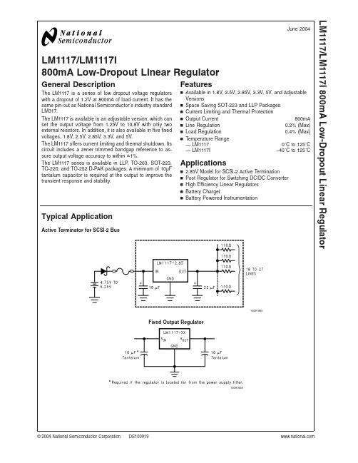
LM1117/LM1117I800mA Low-Dropout Linear RegulatorGeneral DescriptionThe LM1117is a series of low dropout voltage regulators with a dropout of 1.2V at 800mA of load current.It has the same pin-out as National Semiconductor’s industry standard LM317.The LM1117is available in an adjustable version,which can set the output voltage from 1.25V to 13.8V with only two external resistors.In addition,it is also available in five fixed voltages,1.8V,2.5V,2.85V,3.3V,and 5V.The LM1117offers current limiting and thermal shutdown.Its circuit includes a zener trimmed bandgap reference to as-sure output voltage accuracy to within ±1%.The LM1117series is available in LLP ,TO-263,SOT-223,TO-220,and TO-252D-PAK packages.A minimum of 10µF tantalum capacitor is required at the output to improve the transient response and stability.Featuresn Available in 1.8V,2.5V,2.85V,3.3V,5V,and Adjustable Versionsn Space Saving SOT-223and LLP Packages n Current Limiting and Thermal Protection n Output Current 800mA n Line Regulation 0.2%(Max)n Load Regulation 0.4%(Max)n Temperature Range —LM11170˚C to 125˚C —LM1117I −40˚C to 125˚CApplicationsn 2.85V Model for SCSI-2Active Termination n Post Regulator for Switching DC/DC Converter n High Efficiency Linear Regulators n Battery ChargernBattery Powered InstrumentationTypical ApplicationActive Terminator for SCSI-2Bus10091905Fixed Output Regulator10091928June 2004LM1117/LM1117I 800mA Low-Dropout Linear Regulator©2004National Semiconductor Corporation Ordering InformationPackage TemperatureRange Part Number Packaging MarkingTransport Media NSC Drawing 3-lead SOT-2230˚C to +125˚CLM1117MPX-ADJ N03A Tape and Reel MP04ALM1117MPX-1.8N12A Tape and Reel LM1117MPX-2.5N13A Tape and Reel LM1117MPX-2.85N04A Tape and Reel LM1117MPX-3.3N05A Tape and Reel LM1117MPX-5.0N06A Tape and Reel −40˚C to +125˚CLM1117IMPX-ADJ N03B Tape and Reel LM1117IMPX-3.3N05B Tape and Reel LM1117IMPX-5.0N06B Tape and Reel3-lead TO-2200˚C to +125˚CLM1117T-ADJ LM1117T-ADJ Rails T03B LM1117T-1.8LM1117T-1.8Rails LM1117T-2.5LM1117T-2.5Rails LM1117T-2.85LM1117T-2.85Rails LM1117T-3.3LM1117T-3.3Rails LM1117T-5.0LM1117T-5.0Rails 3-lead TO-2520˚C to +125˚CLM1117DTX-ADJ LM1117DT-ADJ Tape and Reel TD03B LM1117DTX-1.8LM1117DT-1.8Tape and Reel LM1117DTX-2.5LM1117DT-2.5Tape and Reel LM1117DTX-2.85LM1117DT-2.85Tape and Reel LM1117DTX-3.3LM1117DT-3.3Tape and Reel LM1117DTX-5.0LM1117DT-5.0Tape and Reel −40˚C to +125˚CLM1117IDTX-ADJ LM1117IDT-ADJ Tape and Reel LM1117IDTX-3.3LM1117IDT-3.3Tape and Reel LM1117IDTX-5.0LM1117IDT-5.0Tape and Reel 8-lead LLP0˚C to +125˚CLM1117LDX-ADJ 1117ADJ Tape and Reel LDC08A LM1117LDX-1.81117-18Tape and Reel LM1117LDX-2.51117-25Tape and Reel LM1117LDX-2.851117-28Tape and Reel LM1117LDX-3.31117-33Tape and Reel LM1117LDX-5.01117-50Tape and Reel −40˚C to 125˚CLM1117ILDX-ADJ 1117IAD Tape and Reel LM1117ILDX-3.31117I33Tape and Reel LM1117ILDX-5.01117I50Tape and Reel TO-2630˚C to +125˚CLM1117SX-ADJ LM1117SADJ Tape and Reel TS3B LM1117SX-2.85LM1117S2.85Tape and Reel LM1117SX-3.3LM1117S3.3Tape and Reel LM1117SX-5.0LM1117S5.0Tape and ReelL M 1117/L M 1117I 2Block Diagram10091901Connection DiagramsSOT-22310091904Top ViewTO-22010091902Top ViewTO-25210091938Top ViewTO-26310091944Top View10091945Side ViewLLP10091946When using the LLP packagePins2,3&4must be connected together andPins5,6&7must be connected togetherTop ViewLM1117/LM1117I3Absolute Maximum Ratings (Note 1)If Military/Aerospace specified devices are required,please contact the National Semiconductor Sales Office/Distributors for availability and specifications.Maximum Input Voltage (V IN to GND)20VPower Dissipation (Note 2)Internally LimitedJunction Temperature (T J )(Note 2)150˚CStorage Temperature Range -65˚C to 150˚CLead TemperatureTO-220(T)Package 260˚C,10sec SOT-223(IMP)Package 260˚C,4secESD Tolerance (Note 3)2000VOperating Ratings (Note 1)Input Voltage (V IN to GND)15VJunction Temperature Range (T J )(Note 2)LM11170˚C to 125˚C LM1117I−40˚C to 125˚CLM1117Electrical CharacteristicsTypicals and limits appearing in normal type apply for T J =25˚C.Limits appearing in Boldface type apply over the entire junc-tion temperature range for operation,0˚C to 125˚C.Symbol Parameter ConditionsMin (Note 5)Typ (Note 4)Max (Note 5)UnitsV REFReference VoltageLM1117-ADJI OUT =10mA,V IN -V OUT =2V,T J =25˚C 10mA ≤I OUT ≤800mA,1.4V ≤V IN -V OUT ≤10V1.2381.2251.2501.2501.2621.270V VV OUTOutput VoltageLM1117-1.8I OUT =10mA,V IN =3.8V,T J =25˚C 0≤I OUT ≤800mA,3.2V ≤V IN ≤10V 1.7821.746 1.8001.800 1.8181.854V V LM1117-2.5I OUT =10mA,V IN =4.5V,T J =25˚C 0≤I OUT ≤800mA,3.9V ≤V IN ≤10V 2.4752.450 2.5002.500 2.5252.550V V LM1117-2.85I OUT =10mA,V IN =4.85V,T J =25˚C 0≤I OUT ≤800mA,4.25V ≤V IN ≤10V 0≤I OUT ≤500mA,V IN =4.10V 2.8202.7902.790 2.8502.8502.850 2.8802.9102.910V V V LM1117-3.3I OUT =10mA,V IN =5V T J =25˚C 0≤I OUT ≤800mA,4.75V ≤V IN ≤10V 3.2673.235 3.3003.300 3.3333.365V V LM1117-5.0I OUT =10mA,V IN =7V,T J =25˚C 0≤I OUT ≤800mA,6.5V ≤V IN ≤12V4.9504.9005.0005.000 5.0505.100V V ∆V OUTLine Regulation (Note 6)LM1117-ADJI OUT =10mA,1.5V ≤V IN -V OUT ≤13.75V 0.0350.2%LM1117-1.8I OUT =0mA,3.2V ≤V IN ≤10V 16mV LM1117-2.5I OUT =0mA,3.9V ≤V IN ≤10V 16mVLM1117-2.85I OUT =0mA,4.25V ≤V IN ≤10V 16mV LM1117-3.3I OUT =0mA,4.75V ≤V IN ≤15V 16mV LM1117-5.0I OUT =0mA,6.5V ≤V IN ≤15V110mVL M 1117/L M 1117I 4LM1117Electrical Characteristics(Continued)Typicals and limits appearing in normal type apply for T J=25˚C.Limits appearing in Boldface type apply over the entire junc-tion temperature range for operation,0˚C to125˚C.Symbol Parameter ConditionsMin(Note5)Typ(Note4)Max(Note5)Units∆V OUT Load Regulation(Note6)LM1117-ADJV IN-V OUT=3V,10≤I OUT≤800mA0.20.4% LM1117-1.8V IN=3.2V,0≤I OUT≤800mA110mVLM1117-2.5V IN=3.9V,0≤I OUT≤800mA110mVLM1117-2.85V IN=4.25V,0≤I OUT≤800mA110mV LM1117-3.3V IN=4.75V,0≤I OUT≤800mA110mV LM1117-5.0V IN=6.5V,0≤I OUT≤800mA115mVV IN-V OUT Dropout Voltage(Note7)I OUT=100mA 1.10 1.20V I OUT=500mA 1.15 1.25V I OUT=800mA 1.20 1.30VI LIMIT Current Limit V IN-V OUT=5V,T J=25˚C80012001500mAMinimum Load Current(Note8)LM1117-ADJV IN=15V 1.75mAQuiescent Current LM1117-1.8V IN≤15V510mALM1117-2.5V IN≤15V510mALM1117-2.85V IN≤10V510mALM1117-3.3V IN≤15V510mALM1117-5.0V IN≤15V510mA Thermal Regulation T A=25˚C,30ms Pulse0.010.1%/W Ripple Regulation f RIPPLE=120Hz,V IN-V OUT=3V V RIPPLE=1V PP6075dB Adjust Pin Current60120µAAdjust Pin Current Change 10≤I OUT≤800mA,1.4V≤V IN-V OUT≤10V0.25µATemperature Stability0.5% Long Term Stability T A=125˚C,1000Hrs0.3% RMS Output Noise(%of V OUT),10Hz≤f≤10kHz0.003%Thermal Resistance Junction-to-Case 3-Lead SOT-22315.0˚C/W 3-Lead TO-220 3.0˚C/W 3-Lead TO-25210˚C/WThermal Resistance Junction-to-Ambient (No air flow)3-Lead SOT-223(No heat sink)136˚C/W3-Lead TO-220(No heat sink)79˚C/W3-Lead TO-252(Note9)(No heat sink)92˚C/W3-Lead TO-26355˚C/W8-Lead LLP(Note10)40˚C/WLM1117/LM1117I5LM1117I Electrical CharacteristicsTypicals and limits appearing in normal type apply for T J =25˚C.Limits appearing in Boldface type apply over the entire junc-tion temperature range for operation,−40˚C to 125˚C.Symbol Parameter ConditionsMin (Note 5)Typ (Note 4)Max (Note 5)UnitsV REFReference VoltageLM1117I-ADJI OUT =10mA,V IN -V OUT =2V,T J =25˚C 10mA ≤I OUT ≤800mA,1.4V ≤V IN -V OUT ≤10V1.2381.2001.2501.2501.2621.290V VV OUTOutput VoltageLM1117I-3.3I OUT =10mA,V IN =5V,T J =25˚C 0≤I OUT ≤800mA,4.75V ≤V IN ≤10V 3.2673.168 3.3003.300 3.3333.432V V LM1117I-5.0I OUT =10mA,V IN =7V,T J =25˚C 0≤I OUT ≤800mA,6.5V ≤V IN ≤12V4.9504.8005.0005.000 5.0505.200V V ∆V OUTLine Regulation (Note 6)LM1117I-ADJI OUT =10mA,1.5V ≤V IN -V OUT ≤13.75V 0.0350.3%LM1117I-3.3I OUT =0mA,4.75V ≤V IN ≤15V 110mV LM1117I-5.0I OUT =0mA,6.5V ≤V IN ≤15V115mV ∆V OUTLoad Regulation (Note 6)LM1117I-ADJV IN -V OUT =3V,10≤I OUT ≤800mA 0.20.5%LM1117I-3.3V IN =4.75V,0≤I OUT ≤800mA 115mV LM1117I-5.0V IN =6.5V,0≤I OUT ≤800mA120mV V IN -V OUTDropout Voltage (Note 7)I OUT =100mA 1.10 1.30V I OUT =500mA 1.15 1.35V I OUT =800mA1.20 1.40V I LIMITCurrent Limit V IN -V OUT =5V,T J =25˚C 80012001500mA Minimum Load Current (Note 8)LM1117I-ADJ V IN =15V 1.75mA Quiescent CurrentLM1117I-3.3V IN ≤15V 515mA LM1117I-5.0V IN ≤15V515mA Thermal Regulation T A =25˚C,30ms Pulse0.010.1%/W Ripple Regulation f RIPPLE =120Hz,V IN -V OUT =3V V RIPPLE =1V PP6075dBAdjust Pin Current 60120µA Adjust Pin Current Change10≤I OUT ≤800mA,1.4V ≤V IN -V OUT ≤10V 0.210µA Temperature Stability 0.5%Long Term Stability T A =125˚C,1000Hrs0.3%RMS Output Noise (%of V OUT ),10Hz ≤f ≤10kHz 0.003%Thermal Resistance Junction-to-Case 3-Lead SOT-22315.0˚C/W 3-Lead TO-25210˚C/W Thermal Resistance Junction-to-Ambient No air flow)3-Lead SOT-223(No heat sink)136˚C/W 3-Lead TO-252(No heat sink)(Note 9)92˚C/W 8-Lead LLP(Note 10)40˚C/WNote 1:Absolute Maximum Ratings indicate limits beyond which damage to the device may occur.Operating Ratings indicate conditions for which the device is intended to be functional,but specific performance is not guaranteed.For guaranteed specifications and the test conditions,see the Electrical Characteristics.L M 1117/L M 1117I 6Note 2:The maximum power dissipation is a function of T J(max),θJA ,and T A .The maximum allowable power dissipation at any ambient temperature is P D =(T J(max)–T A )/θJA .All numbers apply for packages soldered directly into a PC board.Note 3:For testing purposes,ESD was applied using human body model,1.5k Ωin series with 100pF.Note 4:Typical Values represent the most likely parametric norm.Note 5:All limits are guaranteed by testing or statistical analysis.Note 6:Load and line regulation are measured at constant junction room temperature.Note 7:The dropout voltage is the input/output differential at which the circuit ceases to regulate against further reduction in input voltage.It is measured when the output voltage has dropped 100mV from the nominal value obtained at V IN =V OUT +1.5V.Note 8:The minimum output current required to maintain regulation.Note 9:Minimum pad size of 0.038in 2Note 10:Thermal Performance for the LLP was obtained using JESD51-7board with six vias and an ambient temperature of 22˚C.For information about improved thermal performance and power dissipation for the LLP ,refer to Application Note AN-1187.Typical Performance CharacteristicsDropout Voltage (V IN -VOUT )Short-Circuit Current1009192210091923Load Regulation LM1117-ADJ Ripple Rejection1009194310091906LM1117/LM1117I7Typical Performance Characteristics(Continued)LM1117-ADJ Ripple Rejection vs.CurrentTemperature Stability1009190710091925Adjust Pin Current LM1117-2.85Load Transient Response1009192610091908LM1117-5.0Load Transient Response LM1117-2.85Line Transient Response1009190910091910L M 1117/L M 1117I 8Typical Performance Characteristics(Continued) LM1117-5.0Line Transient Response10091911Application Note1.0External Capacitors/Stability1.1Input Bypass CapacitorAn input capacitor is recommended.A10µF tantalum on theinput is a suitable input bypassing for almost all applications.1.2Adjust Terminal Bypass CapacitorThe adjust terminal can be bypassed to ground with a by-pass capacitor(C ADJ)to improve ripple rejection.This by-pass capacitor prevents ripple from being amplified as theoutput voltage is increased.At any ripple frequency,theimpedance of the C ADJ should be less than R1to prevent theripple from being amplified:1/(2π*f RIPPLE*C ADJ)<R1The R1is the resistor between the output and the adjust pin.Its value is normally in the range of100-200Ω.For example,with R1=124Ωand f RIPPLE=120Hz,the C ADJ should be>11µF.1.3Output CapacitorThe output capacitor is critical in maintaining regulator sta-bility,and must meet the required conditions for both mini-mum amount of capacitance and ESR(Equivalent Series Resistance).The minimum output capacitance required by the LM1117is10µF,if a tantalum capacitor is used.Any increase of the output capacitance will merely improve the loop stability and transient response.The ESR of the output capacitor should range between0.3Ω-22Ω.In the case of the adjustable regulator,when the C ADJ is used,a larger output capacitance(22µf tantalum)is required.2.0Output VoltageThe LM1117adjustable version develops a1.25V reference voltage,V REF,between the output and the adjust terminal. As shown in Figure1,this voltage is applied across resistor R1to generate a constant current I1.The current I ADJ from the adjust terminal could introduce error to the output.But since it is very small(60µA)compared with the I1and very constant with line and load changes,the error can be ig-nored.The constant current I1then flows through the output set resistor R2and sets the output voltage to the desired level.For fixed voltage devices,R1and R2are integrated inside the devices.3.0Load RegulationThe LM1117regulates the voltage that appears between itsoutput and ground pins,or between its output and adjustpins.In some cases,line resistances can introduce errors tothe voltage across the load.To obtain the best load regula-tion,a few precautions are needed.Figure2,shows a typical application using a fixed outputregulator.The Rt1and Rt2are the line resistances.It isobvious that the V LOAD is less than the V OUT by the sum ofthe voltage drops along the line resistances.In this case,theload regulation seen at the R LOAD would be degraded fromthe data sheet specification.To improve this,the load shouldbe tied directly to the output terminal on the positive side anddirectly tied to the ground terminal on the negative side.10091917FIGURE1.Basic Adjustable RegulatorLM1117/LM1117I9Application Note(Continued)When the adjustable regulator is used (Figure 3),the best performance is obtained with the positive side of the resistor R1tied directly to the output terminal of the regulator rather than near the load.This eliminates line drops from appearing effectively in series with the reference and degrading regu-lation.For example,a 5V regulator with 0.05Ωresistance between the regulator and load will have a load regulation due to line resistance of 0.05Ωx I L .If R1(=125Ω)is con-nected near the load,the effective line resistance will be 0.05Ω(1+R2/R1)or in this case,it is 4times worse.In addition,the ground side of the resistor R2can be returned near the ground of the load to provide remote ground sens-ing and improve load regulation.4.0Protection DiodesUnder normal operation,the LM1117regulators do not need any protection diode.With the adjustable device,the internal resistance between the adjust and output terminals limits the current.No diode is needed to divert the current around the regulator even with capacitor on the adjust terminal.The adjust pin can take a transient signal of ±25V with respect to the output voltage without damaging the device.When a output capacitor is connected to a regulator and the input is shorted to ground,the output capacitor will discharge into the output of the regulator.The discharge current de-pends on the value of the capacitor,the output voltage of the regulator,and rate of decrease of V IN .In the LM1117regu-lators,the internal diode between the output and input pins can withstand microsecond surge currents of 10A to 20A.With an extremely large output capacitor (≥1000µF),and with input instantaneously shorted to ground,the regulator could be damaged.In this case,an external diode is recommended between the output and input pins to protect the regulator,as shown in Figure 4.5.0Heatsink RequirementsWhen an integrated circuit operates with an appreciable current,its junction temperature is elevated.It is important to quantify its thermal limits in order to achieve acceptable performance and reliability.This limit is determined by sum-ming the individual parts consisting of a series of tempera-ture rises from the semiconductor junction to the operating environment.A one-dimensional steady-state model of con-duction heat transfer is demonstrated in Figure 5.The heat generated at the device junction flows through the die to the die attach pad,through the lead frame to the surrounding case material,to the printed circuit board,and eventually to the ambient environment.Below is a list of variables that may affect the thermal resistance and in turn the need for a heatsink.R θJC (ComponentVariables)R θCA (ApplicationVariables)Leadframe Size &Material Mounting Pad Size,Material,&Location No.of Conduction Pins Placement of Mounting PadDie SizePCB Size &Material Die Attach Material Traces Length &Width Molding Compound Size and MaterialAdjacent Heat Sources Volume of Air Ambient Temperatue Shape of Mounting Pad10091918FIGURE 2.Typical Application using Fixed OutputRegulator 10091919FIGURE 3.Best Load Regulation using AdjustableOutput Regulator 10091915FIGURE 4.Regulator with Protection Diode L M 1117/L M 1117I10Application Note(Continued)The LM1117regulators have internal thermal shutdown to protect the device from over-heating.Under all possible operating conditions,the junction temperature of the LM1117must be within the range of 0˚C to 125˚C.A heatsink may be required depending on the maximum power dissipation and maximum ambient temperature of the application.To deter-mine if a heatsink is needed,the power dissipated by the regulator,P D ,must be calculated:I IN =I L +I GP D =(V IN -V OUT )I L +V IN I GFigure 6shows the voltages and currents which are present in the circuit.The next parameter which must be calculated is the maxi-mum allowable temperature rise,T R (max):T R (max)=T J (max)-T A (max)where T J (max)is the maximum allowable junction tempera-ture (125˚C),and T A (max)is the maximum ambient tem-perature which will be encountered in the application.Using the calculated values for T R (max)and P D ,the maxi-mum allowable value for the junction-to-ambient thermal resistance (θJA )can be calculated:θJA =T R (max)/P DIf the maximum allowable value for θJA is found to be ≥136˚C/W for SOT-223package or ≥79˚C/W for TO-220package or ≥92˚C/W for TO-252package,no heatsink is needed since the package alone will dissipate enough heat to satisfy these requirements.If the calculated value for θJA falls below these limits,a heatsink is required.As a design aid,Table 1shows the value of the θJA of SOT-223and TO-252for different heatsink area.The copper patterns that we used to measure these θJA s are shown at the end of the Application Notes Section.Figure 7and Figure 8reflects the same test results as what are in the Table 1Figure 9and Figure 10shows the maximum allowable power dissipation vs.ambient temperature for the SOT-223and TO-252device.Figures Figure 11and Figure 12shows the maximum allowable power dissipation vs.copper area (in 2)for the SOT-223and TO-252devices.Please see AN1028for power enhancement techniques to be used with SOT-223and TO-252packages.*Application Note AN-1187discusses improved thermal per-formance and power dissipation for the LLP .TABLE 1.θJA Different Heatsink AreaLayout Copper AreaThermal ResistanceTop Side (in 2)*Bottom Side (in 2)(θJA ,˚C/W)SOT-223(θJA ,˚C/W)TO-25210.0123013610320.0660*******.30846040.530755450.76069526106647700.211584800.49870900.689631000.8825711017957120.0660.06612589130.1750.175937210091937FIGURE 5.Cross-sectional view of Integrated Circuit Mounted on a printed circuit board.Note that the case temperature is measured at the point where the leadscontact with the mounting pad surface 10091916FIGURE 6.Power Dissipation DiagramLM1117/LM1117IApplication Note(Continued)TABLE 1.θJA Different Heatsink Area (Continued)Layout Copper AreaThermal Resistance140.2840.2848361150.3920.3927555160.50.57053*Tab of device attached to topside copperL M 1117/L M 1117IApplication Note(Continued)10091913 FIGURE7.θJA vs.1oz Copper Area for SOT-22310091934 FIGURE8.θJA vs.2oz Copper Area for TO-25210091912 FIGURE9.Maximum Allowable Power Dissipation vs.Ambient Temperature for SOT-22310091936FIGURE10.Maximum Allowable Power Dissipation vs.Ambient Temperature for TO-25210091914FIGURE11.Maximum Allowable Power Dissipation vs.1oz Copper Area for SOT-22310091935FIGURE12.Maximum Allowable Power Dissipation vs.2oz Copper Area for TO-252LM1117/LM1117IApplication Note(Continued)10091941FIGURE 13.Top View of the Thermal Test Pattern in Actual ScaleL M 1117/L M 1117IApplication Note(Continued)10091942FIGURE14.Bottom View of the Thermal Test Pattern in Actual Scale LM1117/LM1117ITypical Application Circuits10091930Adjusting Output of Fixed Regulators10091931Regulator with Reference100919291.25V to 10V Adjustable Regulator with ImprovedRipple Rejection100919275V Logic Regulator with Electronic Shutdown*L M 1117/L M 1117ITypical Application Circuits(Continued)10091932Battery Backed-Up Regulated Supply10091933Low Dropout Negative Supply LM1117/LM1117IPhysical Dimensionsinches (millimeters)unless otherwise noted3-Lead SOT-223NS Package Number MP04A3-Lead TO-220NS Package Number T03BL M 1117/L M 1117IPhysical Dimensions inches(millimeters)unless otherwise noted(Continued)3-Lead TO-263NS Package Number TS3B LM1117/LM1117IPhysical Dimensionsinches (millimeters)unless otherwise noted (Continued)3-Lead TO-252NS Package Number TD03B8-Lead LLPNS Package Number LDC08AL M 1117/L M 1117INotesLIFE SUPPORT POLICYNATIONAL’S PRODUCTS ARE NOT AUTHORIZED FOR USE AS CRITICAL COMPONENTS IN LIFE SUPPORT DEVICES OR SYSTEMS WITHOUT THE EXPRESS WRITTEN APPROVAL OF THE PRESIDENT AND GENERAL COUNSEL OF NATIONAL SEMICONDUCTOR CORPORATION.As used herein:1.Life support devices or systems are devices orsystems which,(a)are intended for surgical implant into the body,or(b)support or sustain life,and whose failure to perform when properly used in accordance with instructions for use provided in the labeling,can be reasonably expected to result in a significant injury to the user.2.A critical component is any component of a lifesupport device or system whose failure to perform can be reasonably expected to cause the failure of the life support device or system,or to affect its safety or effectiveness.BANNED SUBSTANCE COMPLIANCENational Semiconductor certifies that the products and packing materials meet the provisions of the Customer Products Stewardship Specification(CSP-9-111C2)and the Banned Substances and Materials of Interest Specification (CSP-9-111S2)and contain no‘‘Banned Substances’’as defined in CSP-9-111S2.National Semiconductor Americas CustomerSupport CenterEmail:new.feedback@ Tel:1-800-272-9959National SemiconductorEurope Customer Support CenterFax:+49(0)180-5308586Email:europe.support@Deutsch Tel:+49(0)6995086208English Tel:+44(0)8702402171Français Tel:+33(0)141918790National SemiconductorAsia Pacific CustomerSupport CenterEmail:ap.support@National SemiconductorJapan Customer Support CenterFax:81-3-5639-7507Email:jpn.feedback@Tel:81-3-5639-7560 LM1117/LM1117I 800mA Low-Dropout Linear RegulatorNational does not assume any responsibility for use of any circuitry described,no circuit patent licenses are implied and National reserves the right at any time without notice to change said circuitry and specifications.。
- 1、下载文档前请自行甄别文档内容的完整性,平台不提供额外的编辑、内容补充、找答案等附加服务。
- 2、"仅部分预览"的文档,不可在线预览部分如存在完整性等问题,可反馈申请退款(可完整预览的文档不适用该条件!)。
- 3、如文档侵犯您的权益,请联系客服反馈,我们会尽快为您处理(人工客服工作时间:9:00-18:30)。
TO-263
温度范围
型号
封装标识
出货形式
0℃~125℃
LM1117MPX-ADJ N03A
编带和卷轴
LM1117MPX-1.8
N12A
编带和卷轴
LM1117MPX-2.5 LM1117MPX-2.85
N13A N04A
编带和卷轴 编带和卷轴
.
LM1117MPX-3.3 LM111 1.250
1.262 1.270
LM1117-1.8
IOUT = 10mA,VIN-VOUT =3.8V, TJ = 25℃
f 0≤IOUT≤800mA, 3.2V≤VIN≤10V
LM1117-2.5
. IOUT = 10mA,VIN-VOUT =4.5V, TJ = 25℃ w 0≤IOUT≤800mA, 3.9V≤VIN≤10V
VREF
参考电压
LM1117I-ADJ
IOUT = 10mA,VIN-VOUT =2V, TJ = 25℃
1.238 1.250 1.262 V
10mA≤IOUT≤800mA, 1.4V≤VIN-VOUT≤ 1.200 1.250 1.290 V
VOUT
10V LM1117I-3.3
.
IOUT = 10mA,VIN-VOUT =5V, TJ = 25℃ 0≤IOUT≤800mA, 4.75V≤VIN≤10V
编带和卷轴 编带和卷轴
wLM1117IDTX-3.3
LM1117IDTX-5.0
LM1117IDT-3.3 LM1117IDT-5.0
编带和卷轴 编带和卷轴
w 0℃~125℃
LM1117LTX-ADJ LM1117LTX-1.8
LM1117LT-ADJ 1117-1.8
编带和卷轴 编带和卷轴
w
LM1117LTX-2.5 LM1117LTX-2.85
a
-LM1117I: -40℃~125℃
LM1117 电气特性
符号
参数
VREF
参考电压
VOUT
输出电压
-
条件
a 最小值 典型值 最大值
LM1117-ADJ IOUT = 10mA,VIN-VOUT =2V, TJ = 25℃
g 10mA≤IOUT≤800mA, 1.4V≤VIN-VOUT≤ p 10V
0.2
5 uA
0.5
%
长期稳定性 TA = 125℃, 1000 小时 RMS 输出噪声 VOUT 的百分比,10Hz≤f≤10kHz
0.3
%
0.003
%
-5-
海纳电子资讯网:www.fpga-arm.com为您提供各种IC的中文资料,应用资料
LM1117I 电气特性
符号
参数
条件
最小值 典型值 最大值 单位
a1
10 mV
VIN = 4.75V, 0≤IOUT≤800mA LM1117-5.0
g1
10 mV
VIN-VOUT 压差
VIN = 6.5V, 0≤IOUT≤800mA IOUT = 100mA
p
1
15 mV
1.10 1.20 V
IOUT = 500mA IOUT = 800mA
f
1.15 1.25 V 1.20 1.30 V
f 高效线性调整器
电池充电器
. 电池供电装置
典型应用
ww SCSI-2 总线有源终端
w
固定电压输出
* 要求调压器远离电源滤波器 -1-
海纳电子资讯网:www.fpga-arm.com为您提供各种IC的中文资料,应用资料
订购信息
封装 3 引脚 SOT-223
3 引脚 SOT-220 3 引脚 SOT-252
续上表
符号
参数
条件
最小值 典型值 最大值 单位
∆VOUT 线性调整率
LM1117-2.85 IOUT = 0mA, 4.25V≤VIN≤10V
1
6 mV
LM1117-3.3
IOUT = 0mA, 4.75V≤VIN≤15V LM1117-5.0
1
6 mV
.
∆VOUT 负载调整率
IOUT = 0mA, 6.5V≤VIN≤15V LM1117-ADJ
1.782 1.746
1.800 1.800
1.818 1.818
2.475 2.450
2.500 2.500
2.525 2.550
单位
V V
V V
V V
LM1117-2.85 IOUT = 10mA,VIN-VOUT =4.85V, TJ = 25℃
w 0≤IOUT≤800mA, 4.25V≤VIN≤10V
1117I50
编带和卷轴
0℃~125℃
LM1117SX-ADJ
LM1117SADJ
编带和卷轴
LM1117SX-2.85
LM1117S2.85
编带和卷轴
LM1117SX-3.3
LM1117S3.3
编带和卷轴
LM1117SX-5.0
LM1117S5.0
编带和卷轴
-2-
海纳电子资讯网:www.fpga-arm.com为您提供各种IC的中文资料,应用资料
4.950 4.900
5.000 5.050 V 5.000 5.100 V
0.035 0.2 %
LM1117-1.8
IOUT = 0mA, 3.2V≤VIN≤10V
1
6 mV
LM1117-2.5
IOUT = 0mA, 3.9V≤VIN≤10V
1
6 mV
-4-
海纳电子资讯网:www.fpga-arm.com为您提供各种IC的中文资料,应用资料
ILIMIT
电流限制 最小负载电流
. VIN-VOUT = 5V, TJ = 25℃
LM1117-ADJ, VIN = 15V
800
1200 1500 mA
1.7
5 mA
空载电流
w LM1117-1.8, VIN≤15V
LM1117-2.5, VIN≤15V
5
10 mA
5
10 mA
w LM1117-2.85, VIN≤10V
1
10 mV
m
VIN-VOUT = 3V, 10≤IOUT≤800mA LM1117-1.8
0.2
r 0.4 %
VIN = 3.2V, 0≤IOUT≤800mA LM1117-2.5
1
a10 mV
VIN = 3.9V, 0≤IOUT≤800mA LM1117-2.85
-1
10 mV
VIN = 4.25V, 0≤IOUT≤800mA LM1117-3.3
pLM1117DT-1.8
LM1117DT-2.5
编带和卷轴 编带和卷轴
f LM1117DTX-2.85
LM1117DTX-3.3
LM1117DT-2.85 LM1117DT-3.3
编带和卷轴 编带和卷轴
-40℃~125℃
. LM1117DTX-5.0
LM1117IDTX-ADJ
LM1117DT-5.0 LM1117IDT-ADJ
g1
15 mV
VIN-VOUT = 3V, 10≤IOUT≤800mA LM1117I-3.3
p
0.2
0.5 %
f VIN = 4.75V, 0≤IOUT≤800mA
LM1117I-5.0
1
15 mV
VIN-VOUT 压差
. VIN = 6.5V, 0≤IOUT≤800mA
IOUT = 100mA
1
3.267 3.168
3.300 3.333 V 3.300 3.432 V
m
LM1117I-5.0 IOUT = 10mA,VIN-VOUT =7V, TJ = 25℃
4.950
5.000
5.050
rV
∆VOUT 线性调整率
0≤IOUT≤800mA, 6.5V≤VIN≤12V LM1117I-ADJ
20 mV
1.10 1.30 V
w IOUT = 500mA
IOUT = 800mA
1.15 1.35 V 1.20 1.40 V
ILIMIT
电流限制 最小负载电流
w VIN-VOUT = 5V, TJ = 25℃
LM1117T-1.8 LM1117T-2.5
-直条
直条
LM1117T-2.85 LM1117T-3.3
LM1117T-2.85 LM1117T-3.3
a直条 直条
0℃~125℃
LM1117T-5.0 LM1117DTX-ADJ
g LM1117T-5.0
LM1117DT-ADJ
直条 编带和卷轴
LM1117DTX-1.8 LM1117DTX-2.5
极限参数
最大输入电压(VIN to GND):20V 结温(TJ):150℃ 储存温度范围:-65℃~150℃
引脚温度:
-TO-220(T)封装:260℃,10 秒 -SOT-223(IMP)封装:260℃,4 秒
.
ESD 保护:2000V
m
工作参数
输入电压(VIN to GND):15V
r
结温(TJ)范围: -LM1117: 0℃~125℃
1117-2.5 1117-2.85
编带和卷轴 编带和卷轴
LM1117LTX-3.3
1117-3.3
编带和卷轴
LM1117LTX-5.0
1117-5.0
编带和卷轴