cd4543b
cd4553
MC14553B3-Digit BCD CounterThe MC14553B 3–digit BCD counter consists of 3 negative edge triggered BCD counters that are cascaded synchronously. A quad latch at the output of each counter permits storage of any given count. The information is then time division multiplexed, providing one BCD number or digit at a time. Digit select outputs provide display control.All outputs are TTL compatible.An on–chip oscillator provides the low–frequency scanning clock which drives the multiplexer output selector.This device is used in instrumentation counters, clock displays,digital panel meters, and as a building block for general logic applications.•TTL Compatible Outputs •On–Chip Oscillator •Cascadable•Clock Disable Input•Pulse Shaping Permits Very Slow Rise Times on Input Clock •Output Latches •Master ResetMAXIMUM RATINGS (Voltages Referenced to V ) (Note 1.)may occur.2.Temperature Derating:Plastic “P and D/DW” Packages: – 7.0 mW/_C From 65_C To 125_C This device contains protection circuitry to guard against damage due to high static voltages or electric fields. However, precautions must be taken to avoid applications of any voltage higher than maximum rated voltages to this high–impedance circuit. For proper operation, V in and V out should be constrained to the range V SS v (V in or V out ) v V DD .Unused inputs must always be tied to an appropriate logic voltage level (e.g.,either V SS or V DD ). Unused outputs must be left open.DevicePackage Shipping ORDERING INFORMATIONMC14553BCP PDIP–1625/Rail MC14553BDWSOIC–1647/Rail查询CD4553 供应商Figure 1. Block Diagram121011139765142115V DD = PIN 16V SS = PIN 8TRUTH TABLE4.The formulas given are for the typical characteristics only at 25_C.5.To calculate total supply current at loads other than 50 pF:I T(C L) = I T(50 pF) + (C L – 50) Vfkwhere: I T is in µA (per package), C L in pF, V = (V DD – V SS) in volts, f in kHz is input frequency, and k = 0.004.7.Data labelled “Typ” is not to be used for design purposes but is intended as an indication of the IC’s potential performance.Figure 2. 3–Digit Counter Timing Diagram (Reference Figure 4)100099999899799699599499399299199090190089910110099989796959493929190898887861716151413121110987654321UNITS CLOCKUNITS Q0UNITS Q1UNITS Q2UNITS Q3TENS CLOCKTENS Q0TENS Q3HUNDREDSCLOCK HUNDREDS Q0HUNDREDS Q3DISABLE OVERFLOW MASTER RESET SCAN OSCILLATOR DIGIT SELECT 1DIGIT SELECT 2DIGIT SELECT 3LLOPERATING CHARACTERISTICSThe MC14553B three–digit counter, shown in Figure 4,consists of three negative edge–triggered BCD counters which are cascaded in a synchronous fashion. A quad latch at the output of each of the three BCD counters permits storage of any given count. The three sets of BCD outputs (active high), after going through the latches, are time division multiplexed, providing one BCD number or digit at a time. Digit select outputs (active low) are provided for display control. All outputs are TTL compatible.An on–chip oscillator provides the low frequency scanning clock which drives the multiplexer output selector.The frequency of the oscillator can be controlled externally by a capacitor between pins 3 and 4, or it can be overridden and driven with an external clock at pin 4. Multiple devices can be cascaded using the overflow output, which provides one pulse for every 1000 counts.The Master Reset input, when taken high, initializes the three BCD counters and the multiplexer scanning circuit.While Master Reset is high the digit scanner is set to digit one; but all three digit select outputs are disabled to prolong display life, and the scan oscillator is inhibited. The Disable input, when high, prevents the input clock from reaching the counters, while still retaining the last count. A pulse shaping circuit at the clock input permits the counters to continue operating on input pulses with very slow rise rmation present in the counters when the latch input goes high, will be stored in the latches and will be retained while the latch input is high, independent of other rmation can be recovered from the latches after the counters have been reset if Latch Enable remains high during the entire reset cycle.Figure 4. Expanded Block DiagramBCD OUTPUTS (ACTIVE HIGH)(ACTIVE HIGH)Figure 5. Six–Digit DisplayS T R O R E S C L O C K I N P U TD I S P L A Y S A RE L O W C U R R E N T L E D s(I p e a k < 10 m A P E R S E G M E N T )PDIP–16P SUFFIX PLASTIC DIP PACKAGENOTES:1.DIMENSIONING AND TOLERANCING PER ANSIY14.5M, 1982.2.CONTROLLING DIMENSION: INCH.3.DIMENSION L TO CENTER OF LEADS WHENFORMED PARALLEL.4.DIMENSION B DOES NOT INCLUDE MOLD FLASH.5.ROUNDED CORNERS OPTIONAL.MDIM MIN MAX MIN MAXMILLIMETERSINCHESA0.7400.77018.8019.55B0.2500.270 6.35 6.85C0.1450.175 3.69 4.44D0.0150.0210.390.53F0.0400.70 1.02 1.77G0.100 BSC 2.54 BSCH0.050 BSC 1.27 BSCJ0.0080.0150.210.38K0.1100.130 2.80 3.30L0.2950.3057.507.74M0 10 0 10S0.0200.0400.51 1.01____SOIC–16DW SUFFIX PLASTIC SOIC PACKAGE CASE 751G–03Notes11NotesON Semiconductor and are trademarks of Semiconductor Components Industries, LLC (SCILLC). SCILLC reserves the right to make changes without further notice to any products herein. SCILLC makes no warranty, representation or guarantee regarding the suitability of its products for any particular purpose, nor does SCILLC assume any liability arising out of the application or use of any product or circuit, and specifically disclaims any and all liability, including without limitation special, consequential or incidental damages. “Typical” parameters which may be provided in SCILLC data sheets and/or specifications can and do vary in different applications and actual performance may vary over time. All operating parameters, including “Typicals” must be validated for each customer application by customer’s technical experts. SCILLC does not convey any license under its patent rights nor the rights of others.SCILLC products are not designed, intended, or authorized for use as components in systems intended for surgical implant into the body, or other applications intended to support or sustain life, or for any other application in which the failure of the SCILLC product could create a situation where personal injury or death may occur. Should Buyer purchase or use SCILLC products for any such unintended or unauthorized application, Buyer shall indemnify and hold SCILLC and its officers, employees, subsidiaries, affiliates, and distributors harmless against all claims, costs, damages, and expenses, and reasonable attorney fees arising out of, directly or indirectly, any claim of personal injury or death associated with such unintended or unauthorized use, even if such claim alleges that SCILLC was negligent regarding the design or manufacture of the part. SCILLC is an Equal Opportunity/Affirmative Action Employer. PUBLICATION ORDERING INFORMATIONCENTRAL/SOUTH AMERICA:Spanish Phone:303–308–7143 (Mon–Fri 8:00am to 5:00pm MST)Email:ONlit–spanish@Toll–Free from Mexico: Dial 01–800–288–2872 for Access –then Dial 866–297–9322ASIA/PACIFIC: LDC for ON Semiconductor – Asia SupportPhone:303–675–2121 (Tue–Fri 9:00am to 1:00pm, Hong Kong Time)Toll Free from Hong Kong & Singapore:001–800–4422–3781Email: ONlit–asia@JAPAN: ON Semiconductor, Japan Customer Focus Center4–32–1 Nishi–Gotanda, Shinagawa–ku, Tokyo, Japan 141–0031Phone: 81–3–5740–2700。
CD4553
数字脉搏测试电路的设计正常人的脉搏次数是每分钟60~80次(婴儿为90~140次,老年人则为100~150次), 这种频率信号属于低频范畴.因此,脉搏计的用来测量低频信号的装置,它的基本功能要求应该是:1.要把人体的脉搏数(振动)转换成电信号,这就需要借助传感器。
2.对转换后的电信号要进行放大和整形处理,以保证其它电路能正常加工和处理。
3.在很短的时间(若干秒)内,测出经放大后的电信号频率值。
总之,脉搏计的核心是要对低频信号在固定的短时间计数,最后以数字形式显示出来。
可见,脉搏计的主要组成部分是计数器和数字显示器。
1 设计思想脉搏计的上述功能要求,可采用两个不同的方案来实现:1.把转换为电信号的脉搏信号,在单位时间内(一分钟或半分钟)进行计数,并用数字显示其计数值,从而直接得到每分钟的脉搏数。
2.测量脉搏跳动固定次数(比如5次,10次)所需的时间,然后转换为没分钟的脉搏数。
这两种方案比较起来,第一种更直观,所需的电路结构更简单些;第二种方案的测量误差比较小,但实现起来电路要复杂些。
为了使脉搏计轻巧而便宜,通常采用第一种方案。
本文进行的设计就基于这一方案。
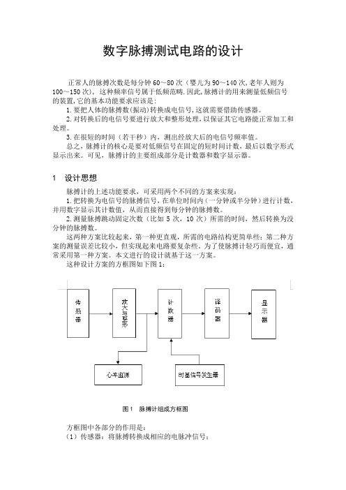
这种设计方案的方框图如下图1:图1 脉搏计组成方框图方框图中各部分的作用是:(1)传感器:将脉搏转换成相应的电脉冲信号;(2)放大电路:对微小电脉冲信号进行放大;(3)时基产生电路:产生固定时间(1分钟或半分钟)的控制信号,作为计数器的门控,使计数器只有在此期间才进行计数;(4)计数、译码、显示电路:在门控信号作用期间,对电脉冲信号进行技术,并显示译码器译码,再由数码管显示计数值;(5)心率监测电路:如果出现心率不齐,应有所告警。
2 功能模块实现2.1 传感器为了把脉搏转换成电信号,应采用压电式传感器。
它有两种基本类型:石英晶体和压电陶瓷。
前者温度稳定性和机械强度都很高,工作温度范围宽,转换精度也高。
而压电陶瓷是人工制造的压电材料。
优点是压电系数大、灵敏度高、价格便宜,只是温度稳定性和强度不如石英晶体。
AC781x 数据手册说明书
版本: 1.3 日期: 2021-12-30© 2013 – 2021 AutoChips Inc.本文档包含杰发科技的专有信息。
未经授权,严禁复制或披露本文档包含的任何信息。
本文档如有更改,不另行通知。
AC781x 数据手册适用于以下产品:型号 子型号环境温度AC7811xxxx AC7811QBGE, AC7811OBGE, AC7811MBGE,AC7811QBFE, AC7811OBFE, AC7811MBFE, AC7811JBFE, AC7811QJGE, AC7811OJGE, AC7811MJGE, AC7811OJFE, AC7811MJFE, AC7811JJFE-40~125°CAC7813xxxx AC7813QBGE, AC7813OBGE, AC7813MBGE, AC7813OBFE, AC7813MBFE, AC7813JBFE -40~85°C AC7815xxxx AC7815QBGE, AC7815OBGE, AC7815MBGE, AC7815QBFE, AC7815OBFE, AC7815MBFE, AC7815JBFE-40~85°C修订记录文档目录修订记录 (2)文档目录 (3)1主要特性 (5)2器件标识 (6)2.1说明 (6)2.2格式 (6)2.3字段 (6)2.4示例 (6)3参数分类 (7)4额定值 (8)4.1热学操作额定值 (8)4.2湿度操作额定值 (8)4.3ESD 操作额定值 (8)4.4电压和电流操作额定值 (9)5通用 (10)5.1静态电气规格 (10)5.1.1电源和地引脚 (10)5.1.2DC 特性 (10)5.1.3电源电流特性 (13)5.2动态规格 (14)5.2.1控制时序 (14)5.2.2PWM模块时序 (15)5.3热规格 (16)5.3.1热特性 (16)6外设工作要求和行为 (18)6.1内核模块 (18)6.1.1SWD 电气规格 (18)6.2外部振荡器 (OSC) 和 ICS 特性 (18)6.2.1外部振荡器(OSC) 特性 (18)6.2.2内部RC 特性 (19)6.2.3PLL 特性 (19)6.3片内Flash 规格 (20)6.4模拟 (21)6.4.1ADC 特性 (21)6.4.2模拟比较器(ACMP)电气规格 (22)6.5通信接口 (22)6.5.1SPI 开关规格 (22)6.5.2CAN特性 (25)7尺寸 (26)7.1LQFP64封装信息 (26)7.2LQFP80封装信息 (28)8引脚分配 (30)8.1信号多路复用和引脚分配 (30)8.2器件引脚分配 (34)1主要特性∙操作特性电压范围:2.7 到5.5 V温度范围 (环境): -40 到125°C∙性能高达100 MHz的 ARM® Cortex-M3内核单周期 32位 x 32位乘法器快速I/O访问接口∙存储器和存储器接口最高256 KB的片内Flash最高 64 KB的静态随机存储器∙时钟振荡器 (Oscillator) –支持4 MHz到 30 MHz 石英晶体振荡器;可选择低功耗或高增益振荡器内部时钟源 (ICS) –内部PLL ,集成内部或外部基准时钟源, 8 MHz预校准内部基准时钟源,可用于100 MHz系统时钟内部32 kHz低功耗振荡器 (LPO)∙系统外设电源管理模块(PMC) 有三个功率模式:运行、待机和停止低压检测复位电路 (LVD)带独立时钟源的看门狗(WDOG)可编程循环冗余校验(CRC)模块串行线调试(SWD) & JTAG 接口Cortex®-M3 嵌入式跟踪宏单元™SRAM 位处理映射区域 (BIT-BAND) 1个12 通道 DMA ∙人机接口68 个通用输入输出接口 (GPIO)外部中断 (IRQ)模块∙模拟模块1个多达 16通道、12位的SAR ADC,工作在停止模式,可选硬件触发器 (ADC)2个包含6位DAC和可编程参考输入的模拟比较器(ACMP)∙定时器1个6通道脉宽调制(PWM)单元3个双通道 PWM1个8通道周期性中断定时器(TIMER)1个脉宽定时器 (PWDT)1个实时时钟 (RTC)∙通信接口2个 SPI 模块6个 UART模块(其中一路兼容Software LIN)2个I2C 模块2个CAN 模块1个硬件 LIN 模块∙封装选项80引脚 LQFP64引脚LQFP2器件标识2.1说明芯片器件型号包含可识别具体器件的字段。
个人贷款担保合同范本(2024年版)版

20XX 专业合同封面COUNTRACT COVER甲方:XXX乙方:XXX个人贷款担保合同范本(2024年版)版本合同目录一览1. 担保合同概述1.1 合同主体1.1.1 贷款人信息1.1.2 借款人信息1.1.3 担保人信息1.2 贷款金额与用途1.3 贷款期限1.4 贷款利率2. 担保方式2.1 抵押担保2.1.1 抵押物描述2.1.2 抵押物权属证明2.1.3 抵押物评估价值2.2 质押担保2.2.1 质押物描述2.2.2 质押物权属证明2.2.3 质押物评估价值2.3 保证担保2.3.1 保证人资格2.3.2 保证范围2.3.3 保证期限3. 担保责任与义务3.1 贷款人的权利与义务3.2 借款人的权利与义务3.3 担保人的权利与义务4. 合同的变更与终止4.1 合同变更4.1.1 变更条件4.1.2 变更程序4.2 合同终止4.2.1 终止条件4.2.2 终止程序5. 违约责任5.1 贷款人的违约责任5.2 借款人的违约责任5.3 担保人的违约责任6. 争议解决6.1 协商解决6.2 调解解决6.3 仲裁解决6.4 诉讼解决7. 合同的生效、修改与解除7.1 合同生效条件7.2 合同修改条件7.3 合同解除条件8. 其他约定8.1 信息保密8.2 法律适用8.3 合同文本8.4 附件9. 签署页9.1 贷款人签署9.2 借款人签署9.3 担保人签署10. 日期11. 合同编号12. 附件清单12.1 抵押物权属证明文件12.2 质押物权属证明文件12.3 其他重要文件13. 补充条款14. 签署人授权证明第一部分:合同如下:第一条担保合同概述1.1 合同主体1.1.1 贷款人信息贷款人全称:_______,统一社会信用代码:_______,地址:_______,联系电话:_______,法定代表人:_______。
1.1.2 借款人信息借款人全称:_______,统一社会信用代码:_______,地址:_______,联系电话:_______,法定代表人:_______。
CD4541中文资料以及PDF引脚功能

CD4541中文资料pdf 引脚功能CD4541/CC4541是一个可编程分频器,它为十六级二分频器。
当脉冲源产生的脉冲信号后,一般其频率较高,这样就需要分频把高频脉冲变换成合适于计时的低频脉冲信号,得到50HZ的脉冲信号。
真值表:比率表:引脚图逻辑图Absolute Maximum Ratings 绝对最大额定值:Supply Voltage电源电压(VDD) −0.5V to +18VInput Voltage输入电压(VIN) −0.5V to VDD +0.5VStorage Temperature Range储存温度范围(TS) −65℃to +150℃Power Dissipation功耗(PD)Recommended Operating Conditions 建议操作条件:DC Electrical Characteristics 直流电气特性:AC Electrical Characteristics 交流电气特性:应用电路:图1 定时电路图此定时电路为声纳浮标定时器,控制系统工作时间长短。
此电路结构简单,定时精确度高,此电路定时控制时间最大为15小时,在电路设计上,V+为电压输入端,输入范围在3~15 V,9 013 代表接面二极管(Junction Diodes),K为6 V继电器,做为控制电路开关。
由于此IC 为频率振荡器,以R(电阻)与C(电容)匹配振荡频率。
其电路设计上之振荡频率匹配须符合1 kHz≤1/(2.3RC)≤100 kHz 及R≥10Ωk,RS≈2R的条件,所以匹配后得到R=150 kΩ,C=4.7 μf,RS=300 kΩ。
在工作时间设定参考(式1)进行设定。
其中时间T 之单位为秒,控制参数n 取值如下表所示,所以欲使系统工作时间达4 小时,其控制参数n 值为8,192,A 与B值皆为0,所以A、B两点均须连接到接地端。
定时电路设定:T = 2.3nRC (式1)。
7400、CD4000系列集成电路管脚及功能表大全
7400、CD4000系列集成电路管脚及功能表大全7400、CD4000系列集成电路管脚及功能表大全7400 TTL 2输入端四与非门7401 TTL 集电极开路2输入端四与非门7402 TTL 2输入端四或非门7403 TTL 集电极开路2输入端四与非门7404 TTL 六反相器7405 TTL 集电极开路六反相器7406 TTL 集电极开路六反相高压驱动器7407 TTL 集电极开路六正相高压驱动器7408 TTL 2输入端四与门7409 TTL 集电极开路2输入端四与门7410 TTL 3输入端3与非门74107 TTL 带清除主从双J-K触发器74109 TTL 带预置清除正触发双J-K触发器7411 TTL 3输入端3与门74112 TTL 带预置清除负触发双J-K触发器7412 TTL 开路输出3输入端三与非门74121 TTL 单稳态多谐振荡器74122 TTL 可再触发单稳态多谐振荡器74123 TTL 双可再触发单稳态多谐振荡器74125 TTL 三态输出高有效四总线缓冲门74126 TTL 三态输出低有效四总线缓冲门7413 TTL 4输入端双与非施密特触发器74132 TTL 2输入端四与非施密特触发器74133 TTL 13输入端与非门74136 TTL 四异或门74138 TTL 3-8线译码器/复工器74139 TTL 双2-4线译码器/复工器7414 TTL 六反相施密特触发器74145 TTL BCD—十进制译码/驱动器7415 TTL 开路输出3输入端三与门74150 TTL 16选1数据选择/多路开关74151 TTL 8选1数据选择器74153 TTL 双4选1数据选择器74154 TTL 4线—16线译码器74155 TTL 图腾柱输出译码器/分配器74156 TTL 开路输出译码器/分配器74157 TTL 同相输出四2选1数据选择器74158 TTL 反相输出四2选1数据选择器7416 TTL 开路输出六反相缓冲/驱动器74160 TTL 可预置BCD异步清除计数器74161 TTL 可予制四位二进制异步清除计数器74162 TTL 可预置BCD同步清除计数器74163 TTL 可予制四位二进制同步清除计数器74164 TTL 八位串行入/并行输出移位寄存器74165 TTL 八位并行入/串行输出移位寄存器74166 TTL 八位并入/串出移位寄存器74169 TTL 二进制四位加/减同步计数器7417 TTL 开路输出六同相缓冲/驱动器74170 TTL 开路输出4×4寄存器堆74173 TTL 三态输出四位D型寄存器74174 TTL 带公共时钟和复位六D触发器74175 TTL 带公共时钟和复位四D触发器74180 TTL 9位奇数/偶数发生器/校验器74181 TTL 算术逻辑单元/函数发生器74185 TTL 二进制—BCD代码转换器74190 TTL BCD同步加/减计数器74191 TTL 二进制同步可逆计数器74192 TTL 可预置BCD双时钟可逆计数器74193 TTL 可预置四位二进制双时钟可逆计数器74194 TTL 四位双向通用移位寄存器74195 TTL 四位并行通道移位寄存器74196 TTL 十进制/二-十进制可预置计数锁存器74197 TTL 二进制可预置锁存器/计数器7420 TTL 4输入端双与非门7421 TTL 4输入端双与门7422 TTL 开路输出4输入端双与非门74221 TTL 双/单稳态多谐振荡器74240 TTL 八反相三态缓冲器/线驱动器74241 TTL 八同相三态缓冲器/线驱动器74243 TTL 四同相三态总线收发器74244 TTL 八同相三态缓冲器/线驱动器74245 TTL 八同相三态总线收发器74247 TTL BCD—7段15V输出译码/驱动器74248 TTL BCD—7段译码/升压输出驱动器74249 TTL BCD—7段译码/开路输出驱动器74251 TTL 三态输出8选1数据选择器/复工器74253 TTL 三态输出双4选1数据选择器/复工器74256 TTL 双四位可寻址锁存器74257 TTL 三态原码四2选1数据选择器/复工器74258 TTL 三态反码四2选1数据选择器/复工器74259 TTL 八位可寻址锁存器/3-8线译码器7426 TTL 2输入端高压接口四与非门74260 TTL 5输入端双或非门74266 TTL 2输入端四异或非门7427 TTL 3输入端三或非门74273 TTL 带公共时钟复位八D触发器74279 TTL 四图腾柱输出S-R锁存器7428 TTL 2输入端四或非门缓冲器74283 TTL 4位二进制全加器74290 TTL 二/五分频十进制计数器74293 TTL 二/八分频四位二进制计数器74295 TTL 四位双向通用移位寄存器74298 TTL 四2输入多路带存贮开关74299 TTL 三态输出八位通用移位寄存器7430 TTL 8输入端与非门7432 TTL 2输入端四或门74322 TTL 带符号扩展端八位移位寄存器74323 TTL 三态输出八位双向移位/存贮寄存器7433 TTL 开路输出2输入端四或非缓冲器74347 TTL BCD—7段译码器/驱动器74352 TTL 双4选1数据选择器/复工器74353 TTL 三态输出双4选1数据选择器/复工器74365 TTL 门使能输入三态输出六同相线驱动器74365 TTL 门使能输入三态输出六同相线驱动器74366 TTL 门使能输入三态输出六反相线驱动器74367 TTL 4/2线使能输入三态六同相线驱动器74368 TTL 4/2线使能输入三态六反相线驱动器7437 TTL 开路输出2输入端四与非缓冲器74373 TTL 三态同相八D锁存器74374 TTL 三态反相八D锁存器74375 TTL 4位双稳态锁存器74377 TTL 单边输出公共使能八D锁存器74378 TTL 单边输出公共使能六D锁存器74379 TTL 双边输出公共使能四D锁存器7438 TTL 开路输出2输入端四与非缓冲器74380 TTL 多功能八进制寄存器7439 TTL 开路输出2输入端四与非缓冲器74390 TTL 双十进制计数器74393 TTL 双四位二进制计数器7440 TTL 4输入端双与非缓冲器7442 TTL BCD—十进制代码转换器74352 TTL 双4选1数据选择器/复工器74353 TTL 三态输出双4选1数据选择器/复工器74365 TTL 门使能输入三态输出六同相线驱动器74366 TTL 门使能输入三态输出六反相线驱动器74367 TTL 4/2线使能输入三态六同相线驱动器74368 TTL 4/2线使能输入三态六反相线驱动器7437 TTL 开路输出2输入端四与非缓冲器74373 TTL 三态同相八D锁存器74374 TTL 三态反相八D锁存器74375 TTL 4位双稳态锁存器74377 TTL 单边输出公共使能八D锁存器74378 TTL 单边输出公共使能六D锁存器74379 TTL 双边输出公共使能四D锁存器7438 TTL 开路输出2输入端四与非缓冲器74380 TTL 多功能八进制寄存器7439 TTL 开路输出2输入端四与非缓冲器74390 TTL 双十进制计数器74393 TTL 双四位二进制计数器7440 TTL 4输入端双与非缓冲器7442 TTL BCD—十进制代码转换器74447 TTL BCD—7段译码器/驱动器7445 TTL BCD—十进制代码转换/驱动器74450 TTL 16:1多路转接复用器多工器74451 TTL 双8:1多路转接复用器多工器74453 TTL 四4:1多路转接复用器多工器7446 TTL BCD—7段低有效译码/驱动器74460 TTL 十位比较器74461 TTL 八进制计数器74465 TTL 三态同相2与使能端八总线缓冲器74466 TTL 三态反相2与使能八总线缓冲器74467 TTL 三态同相2使能端八总线缓冲器74468 TTL 三态反相2使能端八总线缓冲器74469 TTL 八位双向计数器7447 TTL BCD—7段高有效译码/驱动器7448 TTL BCD—7段译码器/内部上拉输出驱动74490 TTL 双十进制计数器74491 TTL 十位计数器74498 TTL 八进制移位寄存器7450 TTL 2-3/2-2输入端双与或非门74502 TTL 八位逐次逼近寄存器74503 TTL 八位逐次逼近寄存器7451 TTL 2-3/2-2输入端双与或非门74533 TTL 三态反相八D锁存器74534 TTL 三态反相八D锁存器7454 TTL 四路输入与或非门74540 TTL 八位三态反相输出总线缓冲器7455 TTL 4输入端二路输入与或非门74563 TTL 八位三态反相输出触发器74564 TTL 八位三态反相输出D触发器74573 TTL 八位三态输出触发器74574 TTL 八位三态输出D触发器74645 TTL 三态输出八同相总线传送接收器74670 TTL 三态输出4×4寄存器堆7473 TTL 带清除负触发双J-K触发器7474 TTL 带置位复位正触发双D触发器7476 TTL 带预置清除双J-K触发器7483 TTL 四位二进制快速进位全加器7485 TTL 四位数字比较器7486 TTL 2输入端四异或门7490 TTL 可二/五分频十进制计数器7493 TTL 可二/八分频二进制计数器7495 TTL 四位并行输入\输出移位寄存器7497 TTL 6位同步二进制乘法器CD系列:CD4000 双3输入端或非门+单非门 TICD4001 四2输入端或非门 HIT/NSC/TI/GOLCD4002 双4输入端或非门 NSCCD4006 18位串入/串出移位寄存器 NSCCD4007 双互补对加反相器 NSCCD4008 4位超前进位全加器 NSCCD4009 六反相缓冲/变换器 NSCCD4010 六同相缓冲/变换器 NSCCD4011 四2输入端与非门 HIT/TICD4012 双4输入端与非门 NSCCD4013 双主-从D型触发器 FSC/NSC/TOSCD4014 8位串入/并入-串出移位寄存器 NSCCD4015 双4位串入/并出移位寄存器 TICD4016 四传输门 FSC/TICD4017 十进制计数/分配器 FSC/TI/MOTCD4018 可预制1/N计数器 NSC/MOTCD4019 四与或选择器 PHICD4020 14级串行二进制计数/分频器 FSCCD4021 08位串入/并入-串出移位寄存器 PHI/NSC CD4022 八进制计数/分配器 NSC/MOTCD4023 三3输入端与非门 NSC/MOT/TICD4024 7级二进制串行计数/分频器 NSC/MOT/TICD4025 三3输入端或非门 NSC/MOT/TICD4026 十进制计数/7段译码器 NSC/MOT/TICD4027 双J-K触发器 NSC/MOT/TICD4028 BCD码十进制译码器 NSC/MOT/TICD4029 可预置可逆计数器 NSC/MOT/TICD4030 四异或门 NSC/MOT/TI/GOLCD4031 64位串入/串出移位存储器 NSC/MOT/TICD4032 三串行加法器 NSC/TICD4033 十进制计数/7段译码器 NSC/TICD4034 8位通用总线寄存器 NSC/MOT/TICD4035 4位并入/串入-并出/串出移位寄存 NSC/MOT/TI CD4038 三串行加法器 NSC/TICD4040 12级二进制串行计数/分频器 NSC/MOT/TICD4041 四同相/反相缓冲器 NSC/MOT/TICD4042 四锁存D型触发器 NSC/MOT/TICD4043 4三态R-S锁存触发器("1"触发) NSC/MOT/TI CD4044 四三态R-S锁存触发器("0"触发) NSC/MOT/TI CD4046 锁相环 NSC/MOT/TI/PHICD4047 无稳态/单稳态多谐振荡器 NSC/MOT/TICD4048 4输入端可扩展多功能门 NSC/HIT/TICD4049 六反相缓冲/变换器 NSC/HIT/TICD4050 六同相缓冲/变换器 NSC/MOT/TICD4051 八选一模拟开关 NSC/MOT/TICD4052 双4选1模拟开关 NSC/MOT/TICD4053 三组二路模拟开关 NSC/MOT/TICD4054 液晶显示驱动器 NSC/HIT/TICD4055 BCD-7段译码/液晶驱动器 NSC/HIT/TICD4056 液晶显示驱动器 NSC/HIT/TICD4059 “N”分频计数器 NSC/TICD4060 14级二进制串行计数/分频器 NSC/TI/MOT CD4063 四位数字比较器 NSC/HIT/TICD4066 四传输门 NSC/TI/MOTCD4067 16选1模拟开关 NSC/TICD4068 八输入端与非门/与门 NSC/HIT/TICD4069 六反相器 NSC/HIT/TICD4070 四异或门 NSC/HIT/TICD4071 四2输入端或门 NSC/TICD4072 双4输入端或门 NSC/TICD4073 三3输入端与门 NSC/TICD4075 三3输入端或门 NSC/TICD4076 四D寄存器CD4077 四2输入端异或非门 HITCD4078 8输入端或非门/或门CD4081 四2输入端与门 NSC/HIT/TICD4082 双4输入端与门 NSC/HIT/TICD4085 双2路2输入端与或非门CD4086 四2输入端可扩展与或非门CD4089 二进制比例乘法器CD4093 四2输入端施密特触发器 NSC/MOT/ST CD4094 8位移位存储总线寄存器 NSC/TI/PHICD4095 3输入端J-K触发器CD4096 3输入端J-K触发器CD4097 双路八选一模拟开关CD4098 双单稳态触发器 NSC/MOT/TICD4099 8位可寻址锁存器 NSC/MOT/STCD40100 32位左/右移位寄存器CD40101 9位奇偶较验器CD40102 8位可预置同步BCD减法计数器CD40103 8位可预置同步二进制减法计数器CD40104 4位双向移位寄存器CD40105 先入先出FI-FD寄存器CD40106 六施密特触发器 NSC\\TICD40107 双2输入端与非缓冲/驱动器 HAR\\TICD40108 4字×4位多通道寄存器CD40109 四低-高电平位移器CD40110 十进制加/减,计数,锁存,译码驱动 STCD40147 10-4线编码器 NSC\\MOTCD40160 可预置BCD加计数器 NSC\\MOTCD40161 可预置4位二进制加计数器 NSC\\MOTCD40162 BCD加法计数器 NSC\\MOTCD40163 4位二进制同步计数器 NSC\\MOTCD40174 六锁存D型触发器 NSC\\TI\\MOTCD40175 四D型触发器 NSC\\TI\\MOTCD40181 4位算术逻辑单元/函数发生器CD40182 超前位发生器CD40192 可预置BCD加/减计数器(双时钟) NSC\\TI CD40193 可预置4位二进制加/减计数器 NSC\\TICD40194 4位并入/串入-并出/串出移位寄存 NSC\\MOT CD40195 4位并入/串入-并出/串出移位寄存 NSC\\MOT CD40208 4×4多端口寄存器CD4501 4输入端双与门及2输入端或非门CD4502 可选通三态输出六反相/缓冲器CD4503 六同相三态缓冲器CD4504 六电压转换器CD4506 双二组2输入可扩展或非门CD4508 双4位锁存D型触发器CD4510 可预置BCD码加/减计数器CD4511 BCD锁存,7段译码,驱动器CD4512 八路数据选择器CD4513 BCD锁存,7段译码,驱动器(消隐) CD4514 4位锁存,4线-16线译码器CD4515 4位锁存,4线-16线译码器CD4516 可预置4位二进制加/减计数器CD4517 双64位静态移位寄存器CD4518 双BCD同步加计数器CD4519 四位与或选择器CD4520 双4位二进制同步加计数器CD4521 24级分频器CD4522 可预置BCD同步1/N计数器CD4526 可预置4位二进制同步1/N计数器CD4527 BCD比例乘法器CD4528 双单稳态触发器CD4529 双四路/单八路模拟开关CD4530 双5输入端优势逻辑门CD4531 12位奇偶校验器CD4532 8位优先编码器CD4536 可编程定时器CD4538 精密双单稳CD4539 双四路数据选择器CD4541 可编程序振荡/计时器CD4543 BCD七段锁存译码,驱动器CD4544 BCD七段锁存译码,驱动器CD4547 BCD七段译码/大电流驱动器CD4549 函数近似寄存器CD4551 四2通道模拟开关CD4553 三位BCD计数器CD4555 双二进制四选一译码器/分离器CD4556 双二进制四选一译码器/分离器CD4558 BCD八段译码器CD4560 "N"BCD加法器CD4561 "9"求补器CD4573 四可编程运算放大器CD4574 四可编程电压比较器CD4575 双可编程运放/比较器CD4583 双施密特触发器CD4584 六施密特触发器CD4585 4位数值比较器CD4599 8位可寻址锁存器CD451174ls46 bcd-七段译码器/驱动器74ls47 bcd-七段译码器/驱动器74ls48 bcd-七段译码器/驱动器74ls49 bcd-七段译码器/驱动器(oc)74ls246 4线-七段译码/驱动器(30v)74ls247 4线-七段译码/驱动器(15v)74ls248 4线-七段译码/驱动器74ls249 4线-七段译码/驱动器74LS电路系列名称解释----------------------------------------------------型号内容---------------------------------------------------- 74ls00 2输入四与非门74ls01 2输入四与非门 (oc)74ls02 2输入四或非门74ls03 2输入四与非门 (oc)74ls04 六倒相器74ls05 六倒相器(oc)74ls06 六高压输出反相缓冲器/驱动器(oc,30v)74ls07 六高压输出缓冲器/驱动器(oc,30v)74ls08 2输入四与门74ls09 2输入四与门(oc)74ls10 3输入三与非门74ls11 3输入三与门74ls12 3输入三与非门 (oc)74ls13 4输入双与非门 (斯密特触发)74ls14 六倒相器(斯密特触发)74ls15 3输入三与门 (oc)74ls16 六高压输出反相缓冲器/驱动器(oc,15v)74ls17 六高压输出缓冲器/驱动器(oc,15v)74ls18 4输入双与非门 (斯密特触发)74ls19 六倒相器(斯密特触发)74ls20 4输入双与非门74ls21 4输入双与门74ls22 4输入双与非门(oc)74ls23 双可扩展的输入或非门74ls24 2输入四与非门(斯密特触发)74ls25 4输入双或非门(有选通)74ls26 2输入四高电平接口与非缓冲器(oc,15v) 74ls27 3输入三或非门74ls28 2输入四或非缓冲器74ls30 8输入与非门74ls31 延迟电路74ls32 2输入四或门74ls33 2输入四或非缓冲器(集电极开路输出) 74ls34 六缓冲器74ls35 六缓冲器(oc)74ls36 2输入四或非门(有选通)74ls37 2输入四与非缓冲器74ls38 2输入四或非缓冲器(集电极开路输出) 74ls39 2输入四或非缓冲器(集电极开路输出) 74ls40 4输入双与非缓冲器74ls41 bcd-十进制计数器74ls42 4线-10线译码器(bcd输入)74ls43 4线-10线译码器(余3码输入)74ls44 4线-10线译码器(余3葛莱码输入) 74ls45 bcd-十进制译码器/驱动器74ls46 bcd-七段译码器/驱动器74ls47 bcd-七段译码器/驱动器74ls48 bcd-七段译码器/驱动器74ls49 bcd-七段译码器/驱动器(oc)74ls50 双二路2-2输入与或非门(一门可扩展) 74ls51 双二路2-2输入与或非门74ls51 二路3-3输入,二路2-2输入与或非门74ls52 四路2-3-2-2输入与或门(可扩展)74ls53 四路2-2-2-2输入与或非门(可扩展) 74ls53 四路2-2-3-2输入与或非门(可扩展) 74ls54 四路2-2-2-2输入与或非门74ls54 四路2-3-3-2输入与或非门74ls54 四路2-2-3-2输入与或非门74ls55 二路4-4输入与或非门(可扩展)74ls60 双四输入与扩展74ls61 三3输入与扩展74ls62 四路2-3-3-2输入与或扩展器74ls63 六电流读出接口门74ls64 四路4-2-3-2输入与或非门74ls65 四路4-2-3-2输入与或非门(oc)74ls70 与门输入上升沿jk触发器74ls71 与输入r-s主从触发器74ls72 与门输入主从jk触发器74ls73 双j-k触发器(带清除端)74ls74 正沿触发双d型触发器(带预置端和清除端)74ls75 4位双稳锁存器74ls76 双j-k触发器(带预置端和清除端)74ls77 4位双稳态锁存器74ls78 双j-k触发器(带预置端,公共清除端和公共时钟端) 74ls80 门控全加器74ls81 16位随机存取存储器74ls82 2位二进制全加器(快速进位)74ls83 4位二进制全加器(快速进位)74ls84 16位随机存取存储器74ls85 4位数字比较器74ls86 2输入四异或门74ls87 四位二进制原码/反码/oi单元74ls89 64位读/写存储器74ls90 十进制计数器74ls91 八位移位寄存器74ls92 12分频计数器(2分频和6分频)74ls93 4位二进制计数器74ls94 4位移位寄存器(异步)74ls95 4位移位寄存器(并行io)74ls96 5位移位寄存器74ls97 六位同步二进制比率乘法器74ls100 八位双稳锁存器74ls103 负沿触发双j-k主从触发器(带清除端)74ls106 负沿触发双j-k主从触发器(带预置,清除,时钟) 74ls107 双j-k主从触发器(带清除端)74ls108 双j-k主从触发器(带预置,清除,时钟)74ls109 双j-k触发器(带置位,清除,正触发)74ls110 与门输入j-k主从触发器(带锁定)74ls111 双j-k主从触发器(带数据锁定)74ls112 负沿触发双j-k触发器(带预置端和清除端) 74ls113 负沿触发双j-k触发器(带预置端)74ls114 双j-k触发器(带预置端,共清除端和时钟端) 74ls116 双四位锁存器74ls120 双脉冲同步器/驱动器74ls121 单稳态触发器(施密特触发)74ls122 可再触发单稳态多谐振荡器(带清除端)74ls123 可再触发双单稳多谐振荡器74ls125 四总线缓冲门(三态输出)74ls126 四总线缓冲门(三态输出)74ls128 2输入四或非线驱动器74ls131 3-8译码器74ls132 2输入四与非门(斯密特触发)74ls133 13输入端与非门74ls134 12输入端与门(三态输出)74ls135 四异或/异或非门74ls136 2输入四异或门(oc)74ls137 八选1锁存译码器/多路转换器74ls138 3-8线译码器/多路转换器74ls139 双2-4线译码器/多路转换器74ls140 双4输入与非线驱动器74ls141 bcd-十进制译码器/驱动器74ls142 计数器/锁存器/译码器/驱动器74ls145 4-10译码器/驱动器74ls147 10线-4线优先编码器74ls148 8线-3线八进制优先编码器74ls150 16选1数据选择器(反补输出)74ls151 8选1数据选择器(互补输出)74ls152 8选1数据选择器多路开关74ls153 双4选1数据选择器/多路选择器74ls154 4线-16线译码器74ls155 双2-4译码器/分配器(图腾柱输出)74ls156 双2-4译码器/分配器(集电极开路输出) 74ls157 四2选1数据选择器/多路选择器74ls158 四2选1数据选择器(反相输出)74ls160 可预置bcd计数器(异步清除)74ls161 可预置四位二进制计数器(并清除异步) 74ls162 可预置bcd计数器(异步清除)74ls163 可预置四位二进制计数器(并清除异步) 74ls164 8位并行输出串行移位寄存器74ls165 并行输入8位移位寄存器(补码输出) 74ls166 8位移位寄存器74ls167 同步十进制比率乘法器74ls168 4位加/减同步计数器(十进制)74ls169 同步二进制可逆计数器74ls170 4*4寄存器堆74ls171 四d触发器(带清除端)74ls172 16位寄存器堆74ls173 4位d型寄存器(带清除端)74ls174 六d触发器74ls175 四d触发器74ls176 十进制可预置计数器74ls177 2-8-16进制可预置计数器74ls178 四位通用移位寄存器74ls179 四位通用移位寄存器74ls180 九位奇偶产生/校验器74ls181 算术逻辑单元/功能发生器74ls182 先行进位发生器74ls183 双保留进位全加器74ls184 bcd-二进制转换器74ls185 二进制-bcd转换器74ls190 同步可逆计数器(bcd,二进制)74ls191 同步可逆计数器(bcd,二进制)74ls192 同步可逆计数器(bcd,二进制)74ls193 同步可逆计数器(bcd,二进制)74ls194 四位双向通用移位寄存器74ls195 四位通用移位寄存器74ls196 可预置计数器/锁存器74ls197 可预置计数器/锁存器(二进制)74ls198 八位双向移位寄存器74ls199 八位移位寄存器74ls210 2-5-10进制计数器74ls213 2-n-10可变进制计数器74ls221 双单稳触发器74ls230 八3态总线驱动器74ls231 八3态总线反向驱动器74ls240 八缓冲器/线驱动器/线接收器(反码三态输出) 74ls241 八缓冲器/线驱动器/线接收器(原码三态输出) 74ls242 八缓冲器/线驱动器/线接收器74ls243 4同相三态总线收发器74ls244 八缓冲器/线驱动器/线接收器74ls245 八双向总线收发器74ls246 4线-七段译码/驱动器(30v)74ls247 4线-七段译码/驱动器(15v)74ls248 4线-七段译码/驱动器74ls249 4线-七段译码/驱动器74ls251 8选1数据选择器(三态输出)74ls253 双四选1数据选择器(三态输出)74ls256 双四位可寻址锁存器74ls257 四2选1数据选择器(三态输出)74ls258 四2选1数据选择器(反码三态输出) 74ls259 8为可寻址锁存器74ls260 双5输入或非门74ls261 4*2并行二进制乘法器74ls265 四互补输出元件74ls266 2输入四异或非门(oc)74ls270 2048位rom (512位四字节,oc) 74ls271 2048位rom (256位八字节,oc) 74ls273 八d触发器74ls274 4*4并行二进制乘法器74ls275 七位片式华莱士树乘法器74ls276 四jk触发器74ls278 四位可级联优先寄存器74ls279 四s-r锁存器74ls280 9位奇数/偶数奇偶发生器/较验器74ls28174ls283 4位二进制全加器74ls290 十进制计数器74ls291 32位可编程模74ls293 4位二进制计数器74ls294 16位可编程模74ls295 四位双向通用移位寄存器74ls298 四-2输入多路转换器(带选通)74ls299 八位通用移位寄存器(三态输出)74ls348 8-3线优先编码器(三态输出)74ls352 双四选1数据选择器/多路转换器74ls353 双4-1线数据选择器(三态输出)74ls354 8输入端多路转换器/数据选择器/寄存器,三态补码输出74ls355 8输入端多路转换器/数据选择器/寄存器,三态补码输出74ls356 8输入端多路转换器/数据选择器/寄存器,三态补码输出74ls357 8输入端多路转换器/数据选择器/寄存器,三态补码输出74ls365 6总线驱动器74ls366 六反向三态缓冲器/线驱动器74ls367 六同向三态缓冲器/线驱动器74ls368 六反向三态缓冲器/线驱动器74ls373 八d锁存器74ls374 八d触发器(三态同相)74ls375 4位双稳态锁存器74ls377 带使能的八d触发器74ls378 六d触发器74ls379 四d触发器74ls381 算术逻辑单元/函数发生器74ls382 算术逻辑单元/函数发生器74ls384 8位*1位补码乘法器74ls385 四串行加法器/乘法器74ls386 2输入四异或门74ls390 双十进制计数器74ls391 双四位二进制计数器74ls395 4位通用移位寄存器74ls396 八位存储寄存器74ls398 四2输入端多路开关(双路输出)74ls399 四-2输入多路转换器(带选通)74ls422 单稳态触发器74ls423 双单稳态触发器74ls440 四3方向总线收发器,集电极开路74ls441 四3方向总线收发器,集电极开路74ls442 四3方向总线收发器,三态输出74ls443 四3方向总线收发器,三态输出74ls444 四3方向总线收发器,三态输出74ls445 bcd-十进制译码器/驱动器,三态输出74ls446 有方向控制的双总线收发器74ls448 四3方向总线收发器,三态输出74ls449 有方向控制的双总线收发器74ls465 八三态线缓冲器74ls466 八三态线反向缓冲器74ls467 八三态线缓冲器74ls468 八三态线反向缓冲器74ls490 双十进制计数器74ls540 八位三态总线缓冲器(反向)74ls541 八位三态总线缓冲器74ls589 有输入锁存的并入串出移位寄存器74ls590 带输出寄存器的8位二进制计数器74ls591 带输出寄存器的8位二进制计数器74ls592 带输出寄存器的8位二进制计数器74ls593 带输出寄存器的8位二进制计数器74ls594 带输出锁存的8位串入并出移位寄存器74ls595 8位输出锁存移位寄存器74ls596 带输出锁存的8位串入并出移位寄存器74ls597 8位输出锁存移位寄存器74ls598 带输入锁存的并入串出移位寄存器74ls599 带输出锁存的8位串入并出移位寄存器74ls604 双8位锁存器74ls605 双8位锁存器74ls606 双8位锁存器74ls607 双8位锁存器74ls620 8位三态总线发送接收器(反相)74ls621 8位总线收发器74ls622 8位总线收发器74ls623 8位总线收发器74ls640 反相总线收发器(三态输出)74ls641 同相8总线收发器,集电极开路74ls642 同相8总线收发器,集电极开路74ls643 8位三态总线发送接收器74ls644 真值反相8总线收发器,集电极开路74ls645 三态同相8总线收发器74ls646 八位总线收发器,寄存器74ls647 八位总线收发器,寄存器74ls648 八位总线收发器,寄存器74ls649 八位总线收发器,寄存器74ls651 三态反相8总线收发器74ls652 三态反相8总线收发器74ls653 反相8总线收发器,集电极开路74ls654 同相8总线收发器,集电极开路74ls668 4位同步加/减十进制计数器74ls669 带先行进位的4位同步二进制可逆计数器74ls670 4*4寄存器堆(三态)74ls671 带输出寄存的四位并入并出移位寄存器74ls672 带输出寄存的四位并入并出移位寄存器74ls673 16位并行输出存储器,16位串入串出移位寄存器74ls674 16位并行输入串行输出移位寄存器74ls681 4位并行二进制累加器74ls682 8位数值比较器(图腾柱输出)74ls683 8位数值比较器(集电极开路)74ls684 8位数值比较器(图腾柱输出)74ls685 8位数值比较器(集电极开路)74ls686 8位数值比较器(图腾柱输出)74ls687 8位数值比较器(集电极开路)74ls688 8位数字比较器(oc输出)74ls689 8位数字比较器74ls690 同步十进制计数器/寄存器(带数选,三态输出,直接清除) 74ls691 计数器/寄存器(带多转换,三态输出)74ls692 同步十进制计数器(带预置输入,同步清除)74ls693 计数器/寄存器(带多转换,三态输出)74ls696 同步加/减十进制计数器/寄存器(带数选,三态输出,直接清除)74ls697 计数器/寄存器(带多转换,三态输出)74ls698 计数器/寄存器(带多转换,三态输出)74ls699 计数器/寄存器(带多转换,三态输出)74ls716 可编程模n十进制计数器74ls718 可编程模n十进制计数器。
惠普HP打印机墨盒通用型号对照表

惠普HP打印机墨盒通用型号对照表HP惠普绘图仪墨盒产品名称产品描述HP C1806A/黑色适用于DJ2000CP/2500CP/2800CP/ 3500CP/3000CP/3500CP/3800CP (户内)HP C1807A/青色适用于DJ2000CP/2500CP/2800CP/ 3500CP/3000CP/3500CP/3800CP (户内)HP C1808A/品红色适用于DJ2000CP/2500CP/2800CP/ 3500CP/3000CP/3500CP/3800CP (户内)HP C1809A/黄色适用于DJ2000CP/2500CP/2800CP/ 3500CP/3000CP/3500CP/3800CP (户内)UV C1892A/黑色适用于DJ2000CP/2500CP/2800CP/ 3500CP/3000CP/3500CP/3800CP (户外)UV C1893A青色适用于DJ2000CP/2500CP/2800CP/ 3500CP/3000CP/3500CP/3800CP (户外)UV C1894A/品红色适用于DJ2000CP/2500CP/2800CP/ 3500CP/3000CP/3500CP/3800CP (户外)UV C1895A/黄色适用于DJ2000CP/2500CP/2800CP/ 3500CP/3000CP/3500CP/3800CP (户外)HP 51626A/黑色适用于DJ200/220/600HP 51640A/黑色适用于DJ230/250/330/350/430/450/455/488/650CHP 51645A/黑色适用于DJ700/750C/750C Plus/755CMHP 51644C/青色适用于DJ350C/450C/455/488/ 750C/750C Plus/755CMHP 51644M/品红色适用于DJ350C/450C/455/488/750C/ 750C Plus/755CMHP 51644Y/黄色适用于DJ350C/450C/455/488/ 750C/750C Plus/755CMHP 51650C/青色适用于DJ250C/650CHP 51650M/品红色适用于HP250C/650CHP 51650Y/黄色适用于DJ250C/650CHP C4871A/黑色适用于DJ1050C/1050CMHP C4871A/青色适用于DJ1050C/1050CMHP C4871A/黄色适用于DJ1050C/1050CMHP C4871A/品红色适用于DJ1050C/1050CMHP C4844A/黑色适用于DJ500/500PS/800/800PSHP C4911A/青色适用于DJ500/500PS/800/800PSHP C4912A/品红色适用于DJ500/500PS/800/800PSHP C4913A/黄色适用于DJ500/500PS/800/800PSHP C4930A/黑色适用于DJ5000/5000PS/5500/5500PS (户内)HP C4940A (户外)HP C3931A/青色适用于DJ5000/5000PS/5500/5500PS (户内)HP C4941A (户外)HP C3932A/品红色适用于DJ5000/5000PS/5500/5500PS (户内)HP C4942A (户外)HP C3933A/黄色适用于DJ5000/5000PS/5500/5500PS (户内)HP C4943A (户外)HP C3934A/浅青色适用于DJ5000/5000PS/5500/5500PS (户内)HP C4944A (户外)HP C3935A/浅红色适用于DJ5000/5000PS/5500/5500PS (户内)HP C4945A (户外)HP惠普喷墨打印机墨盒产品名称产品描述惠普 51625A/彩色适用于HP 200/200Cci/320/340/400/420/500/550/560打印机惠普 51626A/黑色适用于HP 400/420/500/550/560打印机惠普 51629A/黑色适用于HP 600系列打印机/OfficeJet 725打印机惠普 51633M/黑色适用于HP 320/340打印机惠普 51640A/黑色适用于HP 1200打印机惠普 51640C/青色适用于HP 1200/1600C/1600CM 打印机惠普 51640M/品红色适用于HP 1200/1600C/1600CM 打印机惠普 51640Y/黄色适用于HP 1200/1600C/1600CM 打印机惠普 51641A/彩色适用于HP 820Cxi/850Cxi/870/1000打印机惠普51645A/黑色适用于HP 710/820/830/850/870/930/950/970/990/1120/1180/1220/1600 打印机惠普 51649A/彩色适用于HP 600系列打印机惠普 C1823D/彩色适用于HP 710/720/810/830/880/890/895/1120/1125打印机惠普 C1843A/黑色适用于HP 200/220Cci打印机惠普 C4804A/青色适用于HP Inkjet 3000打印机惠普 C4805A/品红色适用于HP Inkjet 3000打印机惠普 C4806A/黄色适用于HP Inkjet 3000打印机惠普 C4810A/浅黑色适用于HP CP1700/1755/2230/2280 打印机惠普 C4811A/浅青色适用于HP CP1700/1755/2230/2280 打印机惠普 C4812A/浅品红色适用于HP CP1700/1755/2230/2280 打印机惠普 C4813A/浅黄色适用于HP CP1700/1755/2230/2280 打印机惠普 C4836A/青色适用于HP CP1700/1755/2230/2280/1100 打印机惠普 C4837A/品红色适用于HP CP1700/1755/2230/2280/1100 打印机惠普 C4838A/黄色适用于HP CP1700/1755/2230/2280/1100 打印机惠普 C4844A/黑色适用于HP CP1700/1755/2230/2280/3000/1100打印机惠普 C6577A/黑色适用于HP 600/610/695cci打印机惠普C6578D/彩色适用于HP 920/930/948/950/970/990/1180/1220/3820/6122/OfficeJet 5110打印机惠普 C6614D/黑色适用于HP 610/630/640/656打印机惠普 C6615D/黑色适用于HP 750/810/840/845/920/948/950/3820/OfficeJet 40/5110打印机惠普 C6625A /彩色适用于HP 840/845打印机惠普 C6656A/黑色适用于HP Photo130/7150/7550/PSC2110/DJ450/5550/OfficeJet 4110打印机惠普 C6657A/彩色适用于HP Photo130/7150/7550/PSC2110/DJ450/5550/OfficeJet 4110打印机惠普 C6658A/彩色适用于HP Photo7150/7550/PSC2110/DJ5550打印机(照片墨盒)惠普 C8816A/黑色适用于HP3558/3658/3668/5168/3538/PSC1118/1218/photo7268打印机惠普 C8817A/彩色适用于HP3558/3538/3658/3668/5168/PSC1118/2329/photo148/7268打印机惠普 C8727A/黑色适用于HP3325/3420打印机惠普 C8728A/彩色适用于HP3325/3420/4110打印机惠普 C9359A 适用于HP photo 148/245/7660/7960HP惠普硒鼓通用一览表产品名称产品描述HP C4182X 适用于LJ 8100/8500系列/8150HP C8061A 适用于LJ 4100系列/4100MFPHP C8061X LJ 4100系列/4100MFPHP C8543X LJ 9000系列/lj9000MFPHP Q2610A LJ 2300系列HP Q1338A LJ 4200系列HP Q1339A LJ 4300系列HP C4092A LJ 1100系列/3200系列HP C4127A LJ 4000/4050系列HP C4127X LJ 4000/4050系列HP C4129X LJ 5000/5100系列HP C4096A LJ 2100/2200系列HP C7115A LJ 1200系列/1000/1005/3300系列/3380HP Q2624A LJ 1150HP Q2612A Color LJ1010/1012/1015/多功能一体机3015/3020/3030 HP Q2613A LJ 1300HP 92298A LJ 4/4M/4 Plus/4M Plus/5/5M/5NHP 92291A LJ IIISI/IIISiMX/4SI/4SIMXHP C3909A LJ 5Si/5SiMX/5SiNX/5Si mopier/8000系列HP C3906F LJ 5L系列/LJ 6L系列/LJ 3100/3150HP C3903F LJ 5P/5MP/6P/6MPHP C3900A LJ 4V/4MVHP 92274A LJ 4L/4ML/4P/4MPHP 92275A LJ IIP/IIP Plus/IIIPHP 92295A LJ II/IID LJ III/IIIDHP C4191A/92A/93A/94A Color 4500/4550系列HP C9720A/21A/22A/23A Color 4600系列HP C4149A/50A/51A/52A Color 8500/8550系列HP C9700A/01A/02A/03A Color 1500/2500系列HP C9730A/31A/32A/33A Color 5500系列HP C8550A/51A/52A/53A Color 9500系列HP Q2670A/71A/72A/73A Color 3500HP Q2670A/81A/82A/83A Color 3700HP Q3683C LJ 9055/9065。
CD4522BE中文资料
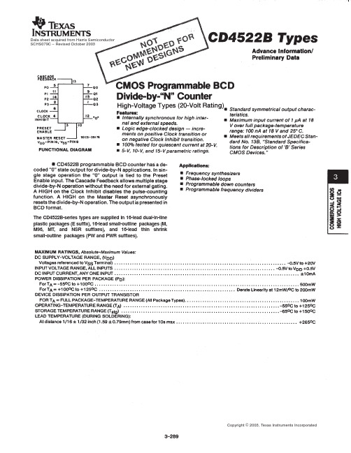
Data sheet acquired from Harris SemiconductorSCHS079C − Revised October 2003The CD4522B-series types are supplied in 16-lead dual-in-line plastic packages (E suffix), 16-lead small-outline packages (M, M96, MT, and NSR suffixes), and 16-lead thin shrink small-outline packages (PW and PWR suffixes).PACKAGING INFORMATIONOrderable Device Status(1)PackageType PackageDrawingPins PackageQtyEco Plan(2)Lead/Ball Finish MSL Peak Temp(3)CD4522BE ACTIVE PDIP N1625Pb-Free(RoHS)CU NIPDAU N/A for Pkg TypeCD4522BEE4ACTIVE PDIP N1625Pb-Free(RoHS)CU NIPDAU N/A for Pkg TypeCD4522BM ACTIVE SOIC D1640Green(RoHS&no Sb/Br)CU NIPDAU Level-1-260C-UNLIMCD4522BM96ACTIVE SOIC D162500Green(RoHS&no Sb/Br)CU NIPDAU Level-1-260C-UNLIMCD4522BM96E4ACTIVE SOIC D162500Green(RoHS&no Sb/Br)CU NIPDAU Level-1-260C-UNLIMCD4522BM96G4ACTIVE SOIC D162500Green(RoHS&no Sb/Br)CU NIPDAU Level-1-260C-UNLIMCD4522BME4ACTIVE SOIC D1640Green(RoHS&no Sb/Br)CU NIPDAU Level-1-260C-UNLIMCD4522BMG4ACTIVE SOIC D1640Green(RoHS&no Sb/Br)CU NIPDAU Level-1-260C-UNLIMCD4522BMT ACTIVE SOIC D16250Green(RoHS&no Sb/Br)CU NIPDAU Level-1-260C-UNLIMCD4522BMTE4ACTIVE SOIC D16250Green(RoHS&no Sb/Br)CU NIPDAU Level-1-260C-UNLIMCD4522BMTG4ACTIVE SOIC D16250Green(RoHS&no Sb/Br)CU NIPDAU Level-1-260C-UNLIMCD4522BNSR ACTIVE SO NS162000Green(RoHS&no Sb/Br)CU NIPDAU Level-1-260C-UNLIMCD4522BNSRE4ACTIVE SO NS162000Green(RoHS&no Sb/Br)CU NIPDAU Level-1-260C-UNLIMCD4522BNSRG4ACTIVE SO NS162000Green(RoHS&no Sb/Br)CU NIPDAU Level-1-260C-UNLIMCD4522BPW ACTIVE TSSOP PW1690Green(RoHS&no Sb/Br)CU NIPDAU Level-1-260C-UNLIMCD4522BPWE4ACTIVE TSSOP PW1690Green(RoHS&no Sb/Br)CU NIPDAU Level-1-260C-UNLIMCD4522BPWG4ACTIVE TSSOP PW1690Green(RoHS&no Sb/Br)CU NIPDAU Level-1-260C-UNLIMCD4522BPWR ACTIVE TSSOP PW162000Green(RoHS&no Sb/Br)CU NIPDAU Level-1-260C-UNLIMCD4522BPWRE4ACTIVE TSSOP PW162000Green(RoHS&no Sb/Br)CU NIPDAU Level-1-260C-UNLIMCD4522BPWRG4ACTIVE TSSOP PW162000Green(RoHS&no Sb/Br)CU NIPDAU Level-1-260C-UNLIM(1)The marketing status values are defined as follows:ACTIVE:Product device recommended for new designs.LIFEBUY:TI has announced that the device will be discontinued,and a lifetime-buy period is in effect.NRND:Not recommended for new designs.Device is in production to support existing customers,but TI does not recommend using this part in a new design.PREVIEW:Device has been announced but is not in production.Samples may or may not be available.OBSOLETE:TI has discontinued the production of the device.(2)Eco Plan-The planned eco-friendly classification:Pb-Free(RoHS),Pb-Free(RoHS Exempt),or Green(RoHS&no Sb/Br)-please check /productcontent for the latest availability information and additional product content details.TBD:The Pb-Free/Green conversion plan has not been defined.Pb-Free(RoHS):TI's terms"Lead-Free"or"Pb-Free"mean semiconductor products that are compatible with the current RoHS requirements for all6substances,including the requirement that lead not exceed0.1%by weight in homogeneous materials.Where designed to be soldered at high temperatures,TI Pb-Free products are suitable for use in specified lead-free processes.Pb-Free(RoHS Exempt):This component has a RoHS exemption for either1)lead-based flip-chip solder bumps used between the die and package,or2)lead-based die adhesive used between the die and leadframe.The component is otherwise considered Pb-Free(RoHS compatible)as defined above.Green(RoHS&no Sb/Br):TI defines"Green"to mean Pb-Free(RoHS compatible),and free of Bromine(Br)and Antimony(Sb)based flame retardants(Br or Sb do not exceed0.1%by weight in homogeneous material)(3)MSL,Peak Temp.--The Moisture Sensitivity Level rating according to the JEDEC industry standard classifications,and peak solder temperature.Important Information and Disclaimer:The information provided on this page represents TI's knowledge and belief as of the date that it is provided.TI bases its knowledge and belief on information provided by third parties,and makes no representation or warranty as to the accuracy of such information.Efforts are underway to better integrate information from third parties.TI has taken and continues to take reasonable steps to provide representative and accurate information but may not have conducted destructive testing or chemical analysis on incoming materials and chemicals.TI and TI suppliers consider certain information to be proprietary,and thus CAS numbers and other limited information may not be available for release.In no event shall TI's liability arising out of such information exceed the total purchase price of the TI part(s)at issue in this document sold by TI to Customer on an annual basis.TAPE AND REELINFORMATION*All dimensionsare nominalDevicePackage Type Package Drawing Pins SPQReel Diameter (mm)Reel Width W1(mm)A0(mm)B0(mm)K0(mm)P1(mm)W (mm)Pin1Quadrant CD4522BM96SOIC D 162500330.016.4 6.510.3 2.18.016.0Q1CD4522BNSR SO NS 162000330.016.48.210.5 2.512.016.0Q1CD4522BPWRTSSOPPW162000330.012.47.05.61.68.012.0Q1PACKAGE MATERIALS INFORMATION19-Mar-2008*All dimensionsare nominalDevice Package TypePackage DrawingPins SPQ Length (mm)Width (mm)Height (mm)CD4522BM96SOIC D 162500333.2345.928.6CD4522BNSR SO NS 162000346.0346.033.0CD4522BPWRTSSOPPW162000346.0346.029.0PACKAGE MATERIALS INFORMATION19-Mar-2008Pack Materials-Page 2IMPORTANT NOTICETexas Instruments Incorporated and its subsidiaries(TI)reserve the right to make corrections,modifications,enhancements,improvements, and other changes to its products and services at any time and to discontinue any product or service without notice.Customers should obtain the latest relevant information before placing orders and should verify that such information is current and complete.All products are sold subject to TI’s terms and conditions of sale supplied at the time of order acknowledgment.TI warrants performance of its hardware products to the specifications applicable at the time of sale in accordance with TI’s standard warranty.Testing and other quality control techniques are used to the extent TI deems necessary to support this warranty.Except where mandated by government requirements,testing of all parameters of each product is not necessarily performed.TI assumes no liability for applications assistance or customer product design.Customers are responsible for their products and applications using TI components.To minimize the risks associated with customer products and applications,customers should provide adequate design and operating safeguards.TI does not warrant or represent that any license,either express or implied,is granted under any TI patent right,copyright,mask work right, or other TI intellectual property right relating to any combination,machine,or process in which TI products or services are rmation published by TI regarding third-party products or services does not constitute a license from TI to use such products or services or a warranty or endorsement e of such information may require a license from a third party under the patents or other intellectual property of the third party,or a license from TI under the patents or other intellectual property of TI.Reproduction of TI information in TI data books or data sheets is permissible only if reproduction is without alteration and is accompanied by all associated warranties,conditions,limitations,and notices.Reproduction of this information with alteration is an unfair and deceptive business practice.TI is not responsible or liable for such altered rmation of third parties may be subject to additional restrictions.Resale of TI products or services with statements different from or beyond the parameters stated by TI for that product or service voids all express and any implied warranties for the associated TI product or service and is an unfair and deceptive business practice.TI is not responsible or liable for any such statements.TI products are not authorized for use in safety-critical applications(such as life support)where a failure of the TI product would reasonably be expected to cause severe personal injury or death,unless officers of the parties have executed an agreement specifically governing such use.Buyers represent that they have all necessary expertise in the safety and regulatory ramifications of their applications,and acknowledge and agree that they are solely responsible for all legal,regulatory and safety-related requirements concerning their products and any use of TI products in such safety-critical applications,notwithstanding any applications-related information or support that may be provided by TI.Further,Buyers must fully indemnify TI and its representatives against any damages arising out of the use of TI products in such safety-critical applications.TI products are neither designed nor intended for use in military/aerospace applications or environments unless the TI products are specifically designated by TI as military-grade or"enhanced plastic."Only products designated by TI as military-grade meet military specifications.Buyers acknowledge and agree that any such use of TI products which TI has not designated as military-grade is solely at the Buyer's risk,and that they are solely responsible for compliance with all legal and regulatory requirements in connection with such use. TI products are neither designed nor intended for use in automotive applications or environments unless the specific TI products are designated by TI as compliant with ISO/TS16949requirements.Buyers acknowledge and agree that,if they use any non-designated products in automotive applications,TI will not be responsible for any failure to meet such requirements.Following are URLs where you can obtain information on other Texas Instruments products and application solutions:Products ApplicationsAmplifiers AudioData Converters AutomotiveDSP BroadbandClocks and Timers Digital ControlInterface MedicalLogic MilitaryPower Mgmt Optical NetworkingMicrocontrollers SecurityRFID TelephonyRF/IF and ZigBee®Solutions Video&ImagingWirelessMailing Address:Texas Instruments,Post Office Box655303,Dallas,Texas75265Copyright©2008,Texas Instruments Incorporated。
- 1、下载文档前请自行甄别文档内容的完整性,平台不提供额外的编辑、内容补充、找答案等附加服务。
- 2、"仅部分预览"的文档,不可在线预览部分如存在完整性等问题,可反馈申请退款(可完整预览的文档不适用该条件!)。
- 3、如文档侵犯您的权益,请联系客服反馈,我们会尽快为您处理(人工客服工作时间:9:00-18:30)。
Data sheet acquired from Harris Semiconductor SCHS086D − Revised April 2004The CD4543B is supplied in 16-lead dual-in-line plasticpackages (E suffix), 16-lead small-outline packages (M, M96,MT , and NSR suffixes), and 16-lead thin shrink small-outlinepackages (PW and PWR suffixes).1PACKAGING INFORMATIONOrderable Device Status(1)PackageType PackageDrawingPins PackageQtyEco Plan(2)Lead/Ball Finish MSL Peak Temp(3)CD4543BE ACTIVE PDIP N1625Pb-Free(RoHS)CU NIPDAU N/A for Pkg TypeCD4543BEE4ACTIVE PDIP N1625Pb-Free(RoHS)CU NIPDAU N/A for Pkg TypeCD4543BM ACTIVE SOIC D1640Green(RoHS&no Sb/Br)CU NIPDAU Level-1-260C-UNLIMCD4543BM96ACTIVE SOIC D162500Green(RoHS&no Sb/Br)CU NIPDAU Level-1-260C-UNLIMCD4543BM96E4ACTIVE SOIC D162500Green(RoHS&no Sb/Br)CU NIPDAU Level-1-260C-UNLIMCD4543BM96G4ACTIVE SOIC D162500Green(RoHS&no Sb/Br)CU NIPDAU Level-1-260C-UNLIMCD4543BME4ACTIVE SOIC D1640Green(RoHS&no Sb/Br)CU NIPDAU Level-1-260C-UNLIMCD4543BMG4ACTIVE SOIC D1640Green(RoHS&no Sb/Br)CU NIPDAU Level-1-260C-UNLIMCD4543BMT ACTIVE SOIC D16250Green(RoHS&no Sb/Br)CU NIPDAU Level-1-260C-UNLIMCD4543BMTE4ACTIVE SOIC D16250Green(RoHS&no Sb/Br)CU NIPDAU Level-1-260C-UNLIMCD4543BMTG4ACTIVE SOIC D16250Green(RoHS&no Sb/Br)CU NIPDAU Level-1-260C-UNLIMCD4543BNSR ACTIVE SO NS162000Green(RoHS&no Sb/Br)CU NIPDAU Level-1-260C-UNLIMCD4543BNSRE4ACTIVE SO NS162000Green(RoHS&no Sb/Br)CU NIPDAU Level-1-260C-UNLIMCD4543BNSRG4ACTIVE SO NS162000Green(RoHS&no Sb/Br)CU NIPDAU Level-1-260C-UNLIMCD4543BPW ACTIVE TSSOP PW1690Green(RoHS&no Sb/Br)CU NIPDAU Level-1-260C-UNLIMCD4543BPWE4ACTIVE TSSOP PW1690Green(RoHS&no Sb/Br)CU NIPDAU Level-1-260C-UNLIMCD4543BPWG4ACTIVE TSSOP PW1690Green(RoHS&no Sb/Br)CU NIPDAU Level-1-260C-UNLIMCD4543BPWR ACTIVE TSSOP PW162000Green(RoHS&no Sb/Br)CU NIPDAU Level-1-260C-UNLIMCD4543BPWRE4ACTIVE TSSOP PW162000Green(RoHS&no Sb/Br)CU NIPDAU Level-1-260C-UNLIMCD4543BPWRG4ACTIVE TSSOP PW162000Green(RoHS&no Sb/Br)CU NIPDAU Level-1-260C-UNLIM(1)The marketing status values are defined as follows:ACTIVE:Product device recommended for new designs.LIFEBUY:TI has announced that the device will be discontinued,and a lifetime-buy period is in effect.NRND:Not recommended for new designs.Device is in production to support existing customers,but TI does not recommend using this part in a new design.PREVIEW:Device has been announced but is not in production.Samples may or may not be available.OBSOLETE:TI has discontinued the production of the device.(2)Eco Plan-The planned eco-friendly classification:Pb-Free(RoHS),Pb-Free(RoHS Exempt),or Green(RoHS&no Sb/Br)-please check /productcontent for the latest availability information and additional product content details.TBD:The Pb-Free/Green conversion plan has not been defined.Pb-Free(RoHS):TI's terms"Lead-Free"or"Pb-Free"mean semiconductor products that are compatible with the current RoHS requirements for all6substances,including the requirement that lead not exceed0.1%by weight in homogeneous materials.Where designed to be soldered at high temperatures,TI Pb-Free products are suitable for use in specified lead-free processes.Pb-Free(RoHS Exempt):This component has a RoHS exemption for either1)lead-based flip-chip solder bumps used between the die and package,or2)lead-based die adhesive used between the die and leadframe.The component is otherwise considered Pb-Free(RoHS compatible)as defined above.Green(RoHS&no Sb/Br):TI defines"Green"to mean Pb-Free(RoHS compatible),and free of Bromine(Br)and Antimony(Sb)based flame retardants(Br or Sb do not exceed0.1%by weight in homogeneous material)(3)MSL,Peak Temp.--The Moisture Sensitivity Level rating according to the JEDEC industry standard classifications,and peak solder temperature.Important Information and Disclaimer:The information provided on this page represents TI's knowledge and belief as of the date that it is provided.TI bases its knowledge and belief on information provided by third parties,and makes no representation or warranty as to the accuracy of such information.Efforts are underway to better integrate information from third parties.TI has taken and continues to take reasonable steps to provide representative and accurate information but may not have conducted destructive testing or chemical analysis on incoming materials and chemicals.TI and TI suppliers consider certain information to be proprietary,and thus CAS numbers and other limited information may not be available for release.In no event shall TI's liability arising out of such information exceed the total purchase price of the TI part(s)at issue in this document sold by TI to Customer on an annual basis.TAPE AND REEL INFORMATION*All dimensions are nominal Device Package Type Package DrawingPinsSPQ Reel Diameter (mm)Reel Width W1(mm)A0(mm)B0(mm)K0(mm)P1(mm)W (mm)Pin1Quadrant CD4543BM96SOICD 162500330.016.4 6.510.3 2.18.016.0Q1CD4543BNSR SONS 162000330.016.48.210.5 2.512.016.0Q1CD4543BPWR TSSOP PW 162000330.012.47.0 5.6 1.68.012.0Q1*All dimensions are nominalDevice Package Type Package Drawing Pins SPQ Length(mm)Width(mm)Height(mm) CD4543BM96SOIC D162500333.2345.928.6 CD4543BNSR SO NS162000346.0346.033.0 CD4543BPWR TSSOP PW162000346.0346.029.0IMPORTANT NOTICETexas Instruments Incorporated and its subsidiaries(TI)reserve the right to make corrections,modifications,enhancements,improvements, and other changes to its products and services at any time and to discontinue any product or service without notice.Customers should obtain the latest relevant information before placing orders and should verify that such information is current and complete.All products are sold subject to TI’s terms and conditions of sale supplied at the time of order acknowledgment.TI warrants performance of its hardware products to the specifications applicable at the time of sale in accordance with TI’s standard warranty.Testing and other quality control techniques are used to the extent TI deems necessary to support this warranty.Except where mandated by government requirements,testing of all parameters of each product is not necessarily performed.TI assumes no liability for applications assistance or customer product design.Customers are responsible for their products and applications using TI components.To minimize the risks associated with customer products and applications,customers should provide adequate design and operating safeguards.TI does not warrant or represent that any license,either express or implied,is granted under any TI patent right,copyright,mask work right, or other TI intellectual property right relating to any combination,machine,or process in which TI products or services are rmation published by TI regarding third-party products or services does not constitute a license from TI to use such products or services or a warranty or endorsement e of such information may require a license from a third party under the patents or other intellectual property of the third party,or a license from TI under the patents or other intellectual property of TI.Reproduction of TI information in TI data books or data sheets is permissible only if reproduction is without alteration and is accompanied by all associated warranties,conditions,limitations,and notices.Reproduction of this information with alteration is an unfair and deceptive business practice.TI is not responsible or liable for such altered rmation of third parties may be subject to additional restrictions.Resale of TI products or services with statements different from or beyond the parameters stated by TI for that product or service voids all express and any implied warranties for the associated TI product or service and is an unfair and deceptive business practice.TI is not responsible or liable for any such statements.TI products are not authorized for use in safety-critical applications(such as life support)where a failure of the TI product would reasonably be expected to cause severe personal injury or death,unless officers of the parties have executed an agreement specifically governing such use.Buyers represent that they have all necessary expertise in the safety and regulatory ramifications of their applications,and acknowledge and agree that they are solely responsible for all legal,regulatory and safety-related requirements concerning their products and any use of TI products in such safety-critical applications,notwithstanding any applications-related information or support that may be provided by TI.Further,Buyers must fully indemnify TI and its representatives against any damages arising out of the use of TI products in such safety-critical applications.TI products are neither designed nor intended for use in military/aerospace applications or environments unless the TI products are specifically designated by TI as military-grade or"enhanced plastic."Only products designated by TI as military-grade meet military specifications.Buyers acknowledge and agree that any such use of TI products which TI has not designated as military-grade is solely at the Buyer's risk,and that they are solely responsible for compliance with all legal and regulatory requirements in connection with such use. TI products are neither designed nor intended for use in automotive applications or environments unless the specific TI products are designated by TI as compliant with ISO/TS16949requirements.Buyers acknowledge and agree that,if they use any non-designated products in automotive applications,TI will not be responsible for any failure to meet such requirements.Following are URLs where you can obtain information on other Texas Instruments products and application solutions:Products ApplicationsAmplifiers AudioData Converters AutomotiveDLP®Products BroadbandDSP Digital ControlClocks and Timers MedicalInterface MilitaryLogic Optical NetworkingPower Mgmt SecurityMicrocontrollers TelephonyRFID Video&ImagingRF/IF and ZigBee®Solutions WirelessMailing Address:Texas Instruments,Post Office Box655303,Dallas,Texas75265Copyright©2009,Texas Instruments Incorporated。