dac8811
铜及铜合金的金相制备

铜的铸造历史悠久,但是直到20世纪 20年代,人们才开始尝试铜及其合 金的热轧及拔丝工艺。现在,大多数 生产的铜均为锻造形式,凭借高导电 性,铜广泛用于电缆、开关元件、变 压器、电动机绕组和发电机等领域。 无氧铜主要用于电子工业。
铜良好的耐腐蚀性和热传导性使其特 别适用于化学、食品和饮料工业的管 路、容器和热交换器等。除了传统的 水管和加热管之外,建筑师们近年来 还发现建筑物外墙若采用氧化铜板结 构会具有非常好的外观。
如制备数据表所示,对于软合金,推 荐用细粒度SiC薄片进行精磨;对于较 硬的合金,可以使用带金刚石的MDLargo。使用MD-Largo可以获得更好 的平整度和边缘保护。
必须通过金刚石抛光除去研磨产生的 所有变形以及嵌入的磨粒。使用二氧 化硅进行化学-机械精抛可以获得几乎 没有任何划痕的表面,因此这种方法 特别重要。对于纯铜,实践证明用含 有硝酸铁的溶液进行终抛可以获得非 常好的结果。对于铜合金,推荐采用 带过氧化氢的OP-S悬浮液和氨水的混 合液(配方见下表)。抛光1分钟后, 在显微镜下检查结果。如有必要,继 续抛光1分钟,并再次检查结果。建议 重复执行此抛光/检查程序,直到获得 要求的质量结果为止。如果抛光过快 或过强,则应该用水稀释混合液。
图15:α-β黄铜铸件,机械抛光,未侵蚀, 放大200x。
图16:试样同图15,电解抛光,未侵蚀, 放大200x。
侵蚀 对铜及铜合金可应用多种侵蚀剂,并且 侵蚀相对比较容易。大多数铸造合金并 不难侵蚀。为某些锻造合金寻找适合的 侵蚀剂则比较困难,特别是当合金进行 过深度冷作时。此时,可以采用着色腐 蚀。 需要注意:铅会被侵蚀剂除去,几乎只 剩下一个个黑洞。在侵蚀之前,必须拍 摄显微照片,确定铅的数量和分布。纯 铅的颜色为灰蓝色。
可控增益放大+电路优化_regina

• 基于乘法器型DAC设计一个可控增益放大器 • 基本要求
– 放大倍数1至128可调,按键控制,步进为4倍循环 – 输入信号1KHz,200mVpp 正弦/方波 – 输出无失真
• 发挥要求
– 自动增益 – 输入信号1KHz,200mVpp-2Vpp间变化 – 输出信号稳定在0.5Vpp
R3
R4
RG
uLM 78 A5
2.5V Reference
VDD = 5V VDD
R3
R4
A4
DOUT ADS7829 CS/SHDN To MSP430
VDD R1 R2
LCL816G
+
A1
R2 R1
1/2 of OPA2337
+
A2
DCLOCK
元器件参数
• 仪表放大器外围的电阻值
– R3 = 400 kW – R4 = 100 kW – RG = 5.33 kW
• OPA2337 = 单电源供电,CMOS,双通道运算放大器 • ADS7829 = 12位,SAR型A/D转换器
电路布局 #1
Op Amp Circuit
ADC Sensor
电路板 #1 底层
ADC采样结果测试 #1
90
Number of Occurrences
80 70 60 50 40
������������������������ ������ode ������in = − × ������ 4096 ������out 4096 = −������in × ������������������������
TI 乘法型DAC
= Parallel
DAC8811中文资料
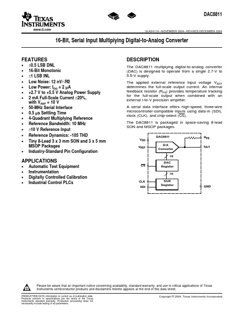
FEATURES DESCRIPTIONAPPLICATIONSR FBI OUTGNDV DDV REFCSCLKSDIDAC8811SLAS411A–NOVEMBER2004–REVISED DECEMBER2004 16-Bit,Serial Input Multiplying Digital-to-Analog Converter•±0.5LSB DNL The DAC8811multiplying digital-to-analog converter •16-Bit Monotonic(DAC)is designed to operate from a single2.7-V to5.5-V supply.•±1LSB INL•Low Noise:12nV/√Hz The applied external reference input voltage VREFdetermines the full-scale output current.An internal •Low Power:I DD=2µAfeedback resistor(R FB)provides temperature tracking •+2.7V to+5.5V Analog Power Supplyfor the full-scale output when combined with an •2mA Full-Scale Current±20%,external I-to-V precision amplifier.with V REF=10VA serial data interface offers high-speed,three-wire•50-MHz Serial Interfacemicrocontroller-compatible inputs using data-in(SDI),•0.5µs Settling Time clock(CLK),and chip-select(CS).•4-Quadrant Multiplying ReferenceThe DAC8811is packaged in space-saving8-lead •Reference Bandwidth:10MHzSON and MSOP packages.•±10V Reference Input•Reference Dynamics:-105THD•Tiny8-Lead3x3mm SON and3x5mmMSOP Packages•Industry-Standard Pin Configuration•Automatic Test Equipment•Instrumentation•Digitally Controlled Calibration•Industrial Control PLCsPlease be aware that an important notice concerning availability,standard warranty,and use in critical applications of TexasInstruments semiconductor products and disclaimers thereto appears at the end of this data sheet.PRODUCTION DATA information is current as of publication date.Copyright©2004,Texas Instruments Incorporated Products conform to specifications per the terms of the TexasInstruments standard warranty.Production processing does notnecessarily include testing of all parameters.元器件交易网ABSOLUTE MAXIMUM RATINGSDAC8811SLAS411A–NOVEMBER 2004–REVISED DECEMBER 2004This integrated circuit can be damaged by ESD.Texas Instruments recommends that all integratedcircuits be handled with appropriate precautions.Failure to observe proper handling and installation procedures can cause damage.ESD damage can range from subtle performance degradation to complete device failure.Precision integrated circuits may be more susceptible to damage because very small parametric changes could cause the device not to meet its published specifications.PACKAGE/ORDERING INFORMATION (1)MINIMUM RELATIVE DIFFERENTIAL PACKAGE-SPECIFIED TRANSPORT ACCURACYNONLINEARITYLEADTEMPERATUREPACKAGE ORDERING MEDIA,PRODUCT (LSB)(LSB)(DESIGNATOR)RANGE MARKINGNUMBER QUANTITY DAC8811C ±1±1MSOP-8(DGK)-40°C to +85°C D11DAC8811ICDGKT Tape and Reel,250DAC8811C ±1±1MSOP-8(DGK)-40°C to +85°C D11DAC8811ICDGKR Tape and Reel,2500DAC8811C ±1±1SON-8(DRB)-40°C to +85°C D11DAC8811ICDRBT Tape and Reel,250DAC8811C ±1±1SON-8(DRB)-40°C to +85°C D11DAC8811ICDRBR Tape and Reel,2500DAC8811B ±2±1MSOP-8(DGK)-40°C to +85°C D11DAC8811IBDGKT Tape and Reel,250DAC8811B ±2±1MSOP-8(DGK)-40°C to +85°C D11DAC8811IBDGKR Tape and Reel,2500DAC8811B ±2±1SON-8(DRB)-40°C to +85°C D11DAC8811IBDRBT Tape and Reel,250DAC8811B±2±1SON-8(DRB)-40°C to +85°CD11DAC8811IBDRBRTape and Reel,2500(1)For the most current specifications and package information,see the Package Option Addendum located at the end of this data sheet or refer to our web site at .over operating free-air temperature range (unless otherwise noted)(1)DAC8811UNIT V DD to GND-0.3to +7V Digital input voltage to GND -0.3to +V DD +0.3V V (I OUT )to GND-0.3to +V DD +0.3V Operating temperature range -40to +105°C Storage temperature range-65to +150°C Junction temperature range (T J max)+125°CPower dissipation (T J max -T A )/R ΘJAThermal impedance,R ΘJA 55°C/W Lead temperature,soldering Vapor phase (60s)215°C Lead temperature,soldering Infrared (15s)220°C ESD rating,HBM 1500V ESD rating,CDM 1000V (1)Stresses above those listed under absolute maximum ratings may cause permanent damage to the device.Exposure to absolute maximum conditions for extended periods may affect device reliability.2元器件交易网ELECTRICAL CHARACTERISTICSDAC8811 SLAS411A–NOVEMBER2004–REVISED DECEMBER2004V DD =+2.7V to+5.5V;IOUT=Virtual GND,GND=0V;VREF=10V;TA=full operating temperature.All specifications-40°Cto+85°C,unless otherwise noted.DAC8811PARAMETER CONDITIONS MIN TYP MAX UNITS STATIC PERFORMANCE(1)Resolution16BitsRelative accuracy DAC8811C±1LSBRelative accuracy DAC8811B±2LSBDifferential nonlinearity±1LSBOutput leakage current Data=0000h,T A=+25°C10nAOutput leakage current Data=0000h,T A=T MAX10nAFull-scale gain error All ones loaded to DAC register±1±4mVFull-scale tempco±3ppm/°COUTPUT CHARACTERISTICS(2)Output current2mAOutput capacitance Code dependent50pFREFERENCE INPUTVREF Range-1515VInput resistance5kΩInput capacitance5pFLOGIC INPUTS AND OUTPUT(2)Input low voltage V IL V DD=+2.7V0.6VV IL V DD=+5V0.8V Input high voltage V IH V DD=+2.7V 2.1VV IH V DD=+5V 2.4V Input leakage current I IL10µAInput capacitance C IL10pFINTERFACE TIMINGClock input frequency f CLK50MHzClock pulse width high10nsClock pulse width low10nsCS to Clock setup time0nsClock to CS hold time10nsData setup time5nsData hold time10nsPOWER REQUIREMENTSV DD 2.7 5.5VI DD(normal operation)Logic inputs=0V5µAV DD=+4.5V to+5.5V V IH=V DD and V IL=GND35µAV DD=+2.7V to+3.6V V IH=V DD and V IL=GND1 2.5µAAC CHARACTERISTICSOutput voltage settling time0.5µsReference multiplying BW V REF=5V PP,Data=FFFFh10MHzV REF=0V to10V,DAC glitch impulse2nV/sData=7FFFh to8000h to7FFFhFeedthrough error V OUT/V REF Data=0000h,V REF=100kHz-70dBDigital feedthrough2nV/s(1)Linearity calculated using a reduced code range of48to4047;output unloaded.(2)Specified by design and characterization;not production tested.3元器件交易网 PIN ASSIGNMENTSDRB PACKAGEDGK PACKAGER VR VDAC8811SLAS411A–NOVEMBER2004–REVISED DECEMBER2004 ELECTRICAL CHARACTERISTICS(continued)V DD =+2.7V to+5.5V;IOUT=Virtual GND,GND=0V;VREF=10V;TA=full operating temperature.All specifications-40°Cto+85°C,unless otherwise noted.DAC8811PARAMETER CONDITIONS MIN TYP MAX UNITS Total harmonic distortion-105dBOutput spot noise voltage12nV/√HzTable1.TERMINAL FUNCTIONSPIN NAME DESCRIPTION1CLK Clock input;positive edge triggered clocks data into shift registerSerial register input;data loads directly into the shift register MSB first.Extra 2SDIleading bits are ignored.3R FB Internal matching feedback resistor.Connect to external op amp output.DAC reference input pin.Establishes DAC full-scale voltage.Constant input 4V REFresistance versus code.DAC current output.Connects to inverting terminal of external precision I/V op 5I OUTamp.6GND Analog and digital ground.7V DD Positive power supply input.Specified operating range of2.7V to5.5V.Chip-select;active low digital input.Transfers shift register data to DAC register 8CSon rising edge.See Table2for operation.4元器件交易网TYPICAL CHARACTERISTICS:V DD =+5V1.00.80.60.40.20−0.2−0.4−0.6−0.8−1.0819216384245763276840960495125734465536I N L (L S B )Digital Input CodeT A =+25_C1.00.80.60.40.20−0.2−0.4−0.6−0.8−1.0D N L (L S B )T A =+25_C819216384245763276840960495125734465536Digital Input Code1.00.80.60.40.20−0.2−0.4−0.6−0.8−1.0T A =−40_CD N L (L S B )819216384245763276840960495125734465536Digital Input Code1.00.80.60.40.20−0.2−0.4−0.6−0.8−1.0T A =−40_CI N L (L S B )819216384245763276840960495125734465536Digital Input Code1.00.80.60.40.20−0.2−0.4−0.6−0.8−1.0I N L (L S B )T A =+85_C819216384245763276840960495125734465536Digital Input Code 1.00.80.60.40.20−0.2−0.4−0.6−0.8−1.0D N L (L S B )T A =+85_C819216384245763276840960495125734465536Digital Input CodeDAC8811SLAS411A–NOVEMBER 2004–REVISED DECEMBER 2004At T A =+25°C,+V DD =+5V,unless otherwise noted.LINEARITY ERROR DIFFERENTIAL LINEARITY ERRORvs DIGITAL INPUT CODEvs DIGITAL INPUT CODEFigure 1.Figure 2.LINEARITY ERROR DIFFERENTIAL LINEARITY ERRORvs DIGITAL INPUT CODEvs DIGITAL INPUT CODEFigure 3.Figure 4.LINEARITY ERROR DIFFERENTIAL LINEARITY ERRORvs DIGITAL INPUT CODEvs DIGITAL INPUT CODEFigure 5.Figure 6.5元器件交易网1.61.41.21.00.80.60.40.2000.51.01.52.02.53.03.54.04.55.0Logic Input Voltage (V)S u p p l y C u r r e n t , I D D (m A )60−6−12−18−24−30−36−42−48−54−60−66−72−78−84−90−96−102−108−114101001k10k100k1M10M100MA t t e n u a t i o n (dB )Bandwidth(Hz)Time (0.1µs/div)O u t p u t V o l t a g e (5V /d i v )Time (0.2µs/div)O u t p u t V o l t a g e (50m V /d i v )DAC8811SLAS411A–NOVEMBER 2004–REVISED DECEMBER 2004TYPICAL CHARACTERISTICS:V DD =+5V (continued)At T A =+25°C,+V DD =+5V,unless otherwise noted.SUPPLY CURRENTvs LOGIC INPUT VOLTAGEREFERENCE MULTIPLYING BANDWIDTHFigure 7.Figure 8.DAC GLITCHDAC SETTLING TIMEFigure 9.Figure 10.6元器件交易网TYPICAL CHARACTERISTICS:V DD =+2.7V1.00.80.60.40.20−0.2−0.4−0.6−0.8−1.0I N L (L S B )T A =+25_C819216384245763276840960495125734465536Digital Input Code1.00.80.60.40.20−0.2−0.4−0.6−0.8−1.0D N L (L S B )T A =+25_C819216384245763276840960495125734465536Digital Input Code1.00.80.60.40.20−0.2−0.4−0.6−0.8−1.0T A =−40_CI N L (L S B )819216384245763276840960495125734465536Digital Input Code T A =−40_C1.00.80.60.40.20−0.2−0.4−0.6−0.8−1.0D N L (L S B )819216384245763276840960495125734465536Digital Input Code1.00.80.60.40.20−0.2−0.4−0.6−0.8−1.0I N L (L S B )T A =+85_C819216384245763276840960495125734465536Digital Input Code 1.00.80.60.40.20−0.2−0.4−0.6−0.8−1.0D N L (L S B )T A =+85_C819216384245763276840960495125734465536Digital Input CodeDAC8811SLAS411A–NOVEMBER 2004–REVISED DECEMBER 2004At T A =+25°C,+V DD =+2.7V,unless otherwise noted.LINEARITY ERROR DIFFERENTIAL LINEARITY ERRORvs DIGITAL INPUT CODEvs DIGITAL INPUT CODEFigure 11.Figure 12.LINEARITY ERROR DIFFERENTIAL LINEARITY ERRORvs DIGITAL INPUT CODEvs DIGITAL INPUT CODEFigure 13.Figure 14.LINEARITY ERROR DIFFERENTIAL LINEARITY ERRORvs DIGITAL INPUT CODEvs DIGITAL INPUT CODEFigure 15.Figure 16.7元器件交易网THEORY OF OPERATIONV REFGNDI OUTV OUT +*V REF CODE65536(1)V OV REFDAC8811SLAS411A–NOVEMBER 2004–REVISED DECEMBER 2004The DAC8811is a single channel current output,16-bit digital-to-analog converter (DAC).The architecture,illustrated in Figure 17,is an R-2R ladder configuration with the three MSBs segmented.Each 2R leg of the ladder is either switched to GND or the I OUT terminal.The I OUT terminal of the DAC is held at a virtual GND potential by the use of an external I/V converter op amp.The R-2R ladder is connected to an external reference input V REF that determines the DAC full-scale current.The R-2R ladder presents a code independent load impedance to the external reference of 5k Ω±25%.The external reference voltage can vary in a range of -15V to 15V,thus providing bipolar I OUT current operation.By using an external I/V converter and the DAC8811R FB resistor,output voltage ranges of -V REF to V REF can be generated.Figure 17.Equivalent R-2R DAC CircuitWhen using an external I/V converter and the DAC8811R FB resistor,the DAC output voltage is given by Equation 1:Each DAC code determines the 2R leg switch position to either GND or I OUT .Because the DAC outputimpedance as seen looking into the I OUT terminal changes versus code,the external I/V converter noise gain will also change.Because of this,the external I/V converter op amp must have a sufficiently low offset voltage such that the amplifier offset is not modulated by the DAC I OUT terminal impedance change.External op amps with large offset voltages can produce INL errors in the transfer function of the DAC8811due to offset modulation versus DAC code.For best linearity performance of the DAC8811,an op amp (OPA277)is recommended (Figure 18).This circuit allows V REF swinging from -10V to +10V.Figure 18.Voltage Output Configuration8元器件交易网SDI CLKCSAPPLICATION INFORMATIONStabilityCircuitV OUTPositive Voltage Output CircuitDAC8811SLAS411A–NOVEMBER 2004–REVISED DECEMBER 2004THEORY OF OPERATION (continued)Figure 19.DAC8811Timing Diagram Table 2.Control Logic Truth Table (1)CLK CS Serial Shift Register DAC Register X H No effectLatched ↑+L Shift register data advanced one bit Latched X H No effectLatchedX ↑+Shift register data transferred to DAC registerNew data loaded from serial register(1)↑+Positive logic transition;X =Don't careTable 3.Serial Input Register Data Format,Data Loaded MSB FirstB15B0Bit (MSB)B14B13B12B11B10B9B8B7B6B5B4B3B2B1(LSB)DataD15D14D13D12D11D10D9D8D7D6D5D4D3D2D1D0For a current-to-voltage design (see Figure 20),the DAC8811current output (I OUT )and the connection with the inverting node of the op amp should be as short as possible and according to correct PCB layout design.For each code change there is a step function.If the GBP of the op amp is limited and parasitic capacitance is excessive at the inverting node then gain peaking is possible.Therefore,for circuit stability,a compensation capacitor C1(4pF to 20pF typ)can be added to the design,as shown in Figure 20.Figure 20.Gain Peaking Prevention Circuit With Compensation CapacitorAs Figure 21illustrates,in order to generate a positive voltage output,a negative reference is input to the DAC8811.This design is suggested instead of using an inverting amp to invert the output due to tolerance errors of the resistor.For a negative reference,V OUT and GND of the reference are level-shifted to a virtual ground and a -2.5V input to the DAC8811with an op amp.9元器件交易网V OUTBipolar Output CircuitV OUT+ǒD32,768*1ǓV REF(2)V OUT10 k W10 k W+2.5V(+10V)Programmable Current Source CircuitI L +(R2)R3)ńR1R3VREFD(3)DAC8811SLAS411A–NOVEMBER2004–REVISED DECEMBER2004APPLICATION INFORMATION(continued)Figure21.Positive Voltage Output CircuitThe DAC8811,as a2-quadrant multiplying DAC,can be used to generate a unipolar output.The polarity of the full-scale output I OUT is the inverse of the input reference voltage at V REF.Some applications require full4-quadrant multiplying capabilities or bipolar output swing.As shown in Figure22, external op amp U4is added as a summing amp and has a gain of2X that widens the output span to5V.A 4-quadrant multiplying circuit is implemented by using a 2.5-V offset of the reference voltage to bias U4.According to the circuit transfer equation given in Equation2,input data(D)from code0to full scale produces output voltages of V OUT=-2.5V to V OUT=+2.5V.External resistance mismatching is the significant error in Figure22.Figure22.Bipolar Output CircuitA DAC8811can be integrated into the circuit in Figure23to implement an improved Howland current pump forprecise voltage to current conversions.Bidirectional current flow and high voltage compliance are two features of the circuit.With a matched resistor network,the load current of the circuit is shown by Equation3:10元器件交易网ZO+R1ȀR3(R1)R2)R1(R2Ȁ)R3Ȁ)*R1Ȁ(R2)R3)(4)V REFR244OUTCross-ReferenceDAC8811 SLAS411A–NOVEMBER2004–REVISED DECEMBER2004The value of R3in the previous equation can be reduced to increase the output current drive of U3.U3can drive ±20mA in both directions with voltage compliance limited up to15V by the U3voltage supply.Elimination of the circuit compensation capacitor C1in the circuit is not suggested as a result of the change in the output impedance Z O,according to Equation4:As shown in Equation4,with matched resistors,Z O is infinite and the circuit is optimum for use as a current source.However,if unmatched resistors are used,Z O is positive or negative with negative output impedance being a potential cause of oscillation.Therefore,by incorporating C1into the circuit,possible oscillation problems are eliminated.The value of C1can be determined for critical applications;for most applications,however,a value of several pF is suggested.Figure23.Programmable Bidirectional Current Source CircuitThe DAC8811has an industry-standard pinout.Table4provides the cross-reference information.Table4.Cross-ReferenceSPECIFIEDTEMPERATURE PACKAGE PACKAGE CROSS-PRODUCT INL(LSB)DNL(LSB)RANGE DESCRIPTION OPTION REFERENCE PART DAC8811ICDGK±1±1-40°C to+85°C8-Lead MicroSOIC MSOP-8N/ADAC8811IBDGK±2±1-40°C to+85°C8-Lead MicroSOIC MSOP-8AD5543BRMDAC8811ICDRB±1±1-40°C to+85°C8-Lead Small Outline SON-8N/ADAC8811IBDRD±2±1-40°C to+85°C8-Lead Small Outline SON-8N/A N/A±2±1-40°C to+85°C8-Lead SOIC SOIC-8AD5543BR11元器件交易网PACKAGING INFORMATIONOrderable Device Status (1)Package Type Package Drawing Pins Package Qty Eco Plan (2)Lead/Ball FinishMSL Peak Temp (3)DAC8811IBDGKR ACTIVE MSOP DGK 82500TBD Call TI Call TIDAC8811IBDGKT ACTIVE MSOP DGK 8250TBD Call TILevel-1-220C-UNLIMDAC8811IBDRBR ACTIVE SON DRB 83000TBD CU POST PLATE Level-1-240C-UNLIM DAC8811IBDRBT ACTIVE SON DRB 8250TBD CU POST PLATE Level-1-240C-UNLIMDAC8811ICDGKR ACTIVE MSOP DGK 82500TBD Call TI Level-1-220C-UNLIM DAC8811ICDGKT ACTIVE MSOP DGK 8250TBD Call TI Level-1-220C-UNLIM DAC8811ICDRBR ACTIVE SON DRB 83000TBD CU SNPB Level-1-240C-UNLIM DAC8811ICDRBTACTIVESONDRB8250TBDCU SNPBLevel-1-240C-UNLIM(1)The marketing status values are defined as follows:ACTIVE:Product device recommended for new designs.LIFEBUY:TI has announced that the device will be discontinued,and a lifetime-buy period is in effect.NRND:Not recommended for new designs.Device is in production to support existing customers,but TI does not recommend using this part in a new design.PREVIEW:Device has been announced but is not in production.Samples may or may not be available.OBSOLETE:TI has discontinued the production of the device.(2)Eco Plan -The planned eco-friendly classification:Pb-Free (RoHS)or Green (RoHS &no Sb/Br)-please check /productcontent for the latest availability information and additional product content details.TBD:The Pb-Free/Green conversion plan has not been defined.Pb-Free (RoHS):TI's terms "Lead-Free"or "Pb-Free"mean semiconductor products that are compatible with the current RoHS requirements for all 6substances,including the requirement that lead not exceed 0.1%by weight in homogeneous materials.Where designed to be soldered at high temperatures,TI Pb-Free products are suitable for use in specified lead-free processes.Green (RoHS &no Sb/Br):TI defines "Green"to mean Pb-Free (RoHS compatible),and free of Bromine (Br)and Antimony (Sb)basedflame retardants (Br or Sb do not exceed 0.1%by weight in homogeneous material)(3)MSL,Peak Temp.--The Moisture Sensitivity Level rating according to the JEDEC industry standard classifications,and peak solder temperature.Important Information and Disclaimer:The information provided on this page represents TI's knowledge and belief as of the date that it is provided.TI bases its knowledge and belief on information provided by third parties,and makes no representation or warranty as to the accuracy of such information.Efforts are underway to better integrate information from third parties.TI has taken and continues to take reasonable steps to provide representative and accurate information but may not have conducted destructive testing or chemical analysis on incoming materials and chemicals.TI and TI suppliers consider certain information to be proprietary,and thus CAS numbers and other limited information may not be available for release.In no event shall TI's liability arising out of such information exceed the total purchase price of the TI part(s)at issue in this document sold by TI to Customer on an annual basis.PACKAGE OPTION ADDENDUM17-Jun-2005Addendum-Page 1IMPORTANT NOTICETexas Instruments Incorporated and its subsidiaries (TI) reserve the right to make corrections, modifications, enhancements, improvements, and other changes to its products and services at any time and to discontinue any product or service without notice. Customers should obtain the latest relevant information before placing orders and should verify that such information is current and complete. All products are sold subject to TI’s terms and conditions of sale supplied at the time of order acknowledgment.TI warrants performance of its hardware products to the specifications applicable at the time of sale in accordance with TI’s standard warranty. T esting and other quality control techniques are used to the extent TI deems necessary to support this warranty. Except where mandated by government requirements, testing of all parameters of each product is not necessarily performed.TI assumes no liability for applications assistance or customer product design. Customers are responsible for their products and applications using TI components. T o minimize the risks associated with customer products and applications, customers should provide adequate design and operating safeguards.TI does not warrant or represent that any license, either express or implied, is granted under any TI patent right, copyright, mask work right, or other TI intellectual property right relating to any combination, machine, or process in which TI products or services are used. Information published by TI regarding third-party products or services does not constitute a license from TI to use such products or services or a warranty or endorsement thereof. Use of such information may require a license from a third party under the patents or other intellectual property of the third party, or a license from TI under the patents or other intellectual property of TI.Reproduction of information in TI data books or data sheets is permissible only if reproduction is without alteration and is accompanied by all associated warranties, conditions, limitations, and notices. Reproduction of this information with alteration is an unfair and deceptive business practice. TI is not responsible or liable for such altered documentation.Resale of TI products or services with statements different from or beyond the parameters stated by TI for that product or service voids all express and any implied warranties for the associated TI product or service and is an unfair and deceptive business practice. TI is not responsible or liable for any such statements. Following are URLs where you can obtain information on other Texas Instruments products and application solutions:Products ApplicationsAmplifiers Audio /audioData Converters Automotive /automotiveDSP Broadband /broadbandInterface Digital Control /digitalcontrolLogic Military /militaryPower Mgmt Optical Networking /opticalnetwork Microcontrollers Security /securityTelephony /telephonyVideo & Imaging /videoWireless /wirelessMailing Address:Texas InstrumentsPost Office Box 655303 Dallas, Texas 75265Copyright 2005, Texas Instruments Incorporated。
Zynq的PS端的SPI

Zynq的PS端的SPIZynq 赛灵思公司(Xilinx)推出的⾏业第⼀个可扩展处理平台Zynq系列。
旨在为视频监视、汽车驾驶员辅助以及⼯⼚⾃动化等⾼端嵌⼊式应⽤提供所需的处理与计算性能⽔平。
Zynq中包含FPGA资源和ARM资源,可⽤AXI⽚内总线进⾏互联。
PS端的SPI 在zynq中,PS端有两个SPI控制器,每个控制器可以接3个设备,因为zynq除了ARM之外,还含有FPGA资源,因此可以利⽤FPGA资源将SPI控制器可控制的设备进⾏⼀个扩展,本次在使⽤SPI中遇到了⼀些问题,在此记下。
使⽤SPI控制DAC8811的问题描述 设计中,做了⼀个程控放⼤器,采⽤的芯⽚是DAC8811,这个芯⽚是采⽤SPI进⾏通讯,它⾥⾯是⼀个16位的寄存器,每次通过SPI写这个16位的寄存器就可以达到调整输出的⽬的。
但是使⽤zynq的SPI控制控制该设备后,因为zynq提供的SPI的裸机驱动,每次只能发送⼀个字节,因此控制DAC8811的寄存器更新需要发送两个字节。
我使⽤spi连续发送两个字节后,程控放⼤器的放⼤倍数和我设置的有区别,更改写⼊的值出现貌似⽆规律的跳变,⽆法对该芯⽚进⾏正常的控制。
原因 将spi输出的信号利⽤⽰波器进⾏观察,发现似乎并没有什么⽑病,于是我将时钟信号和⽚选信号都进⾏观察,利⽤⽚选信号的上升沿捕捉信号,发现在发送了第⼀个字节后发第⼆个⾃字节的中间,⽚选信号由低电平跳变为⾼电平,这个时间是很短的,可以认为这是⼀个⾼频信号。
⽽DAC8811在⽚选信号上升沿时将会将寄存器中的值更新到输出,这样实际上就是寄存器只接收了⼀个字节就更新了,本来是应该接收两个字节后更新的。
查看zynq的spi代码,⾥⾯是有设置各个延时的函数的,但是设置了延时到最⼩值,还是会出现着这样的问题。
解决⽅案 ⽅案⼀:使⽤zynq的PL资源写⼀个⾼频滤波器,对⽚选信号进⾏滤波,已达到将⾼频跳变去除。
⽅案⼆:⾼频的东西滤除更简单的是使⽤电容,根据容抗的计算公式: 电容值越⼩,容抗越⼤,在这⾥将⽚选信号线对地接⼀个2nF的电容即可达到⽬的。
DAC选型手册
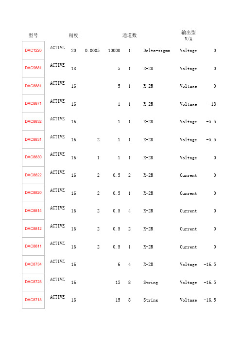
精度通道数输出型V/A200.0005100001 Delta-sigma Voltage 018 51 R-2R Voltage 016 51 R-2R Voltage 016 11 R-2R Voltage -1816 11 R-2R Voltage -5.516211 R-2R Voltage -5.516111 R-2R Voltage 01620.52 R-2R Current 01620.51 R-2R Current 01620.54 R-2R Current 01620.52 R-2R Current 01620.51 R-2R Current 016 64 R-2R Voltage -16.516 158 String Voltage -16.516 158 String Voltage -16.51630.651 String Voltage -5.516160.651 String Voltage -6160.043104 String Voltage -6160.043101 String Voltage 016 58 String Voltage 0160.284 String Voltage 0160.284 String Voltage 0 DAC856216 72 String Voltage 0160.281 String Voltage 0160.2104 String Voltage 0160.2104 String Voltage 0160.2102 String Voltage 0160.2101 String Voltage 0160.2101 String Voltage 016 84 String Voltage 0160.1101 String Voltage 0160.093104 String Voltage 0160.093102 String Voltage 0160.093101 String Voltage 0160.093101 String Voltage 016 61 String Voltage 0160.1104 R-2R Voltage -10160.251 R-2R Voltage -10160.251 R-2R Voltage -10160.089104 R-2R Voltage -10160.17251 R-2R Voltage -10160.1124 R-2R Voltage -2.5160.1124 R-2R Voltage -2.5160.1104 R-2R Voltage -2.5160.1102 R-2R Voltage -2.5160.1101 R-2R Voltage -2.5160.089104 R-2R Voltage -2.5160.089102 R-2R Voltage -2.5160.093101 R-2R Voltage -2.5160.086101 R-2R Voltage 0160.1101 R-2R Voltage 0160.086101 R-2R Voltage -10160.1101 R-2R Voltage -10168000.0112 Current sink Current 2168000.0112 Current sink Current 2165000.0122 Current sink Current 2165000.0122 Current sink Current 21610000.01042 Current sink Current 21610000.01041 Current sink Current 21610000.01041 Current sink Current 2168000.01042 Current sink Current 2166250.01042 Current sink Current 2160.000520001 Delta-sigma Voltage 0141250.0351 Current source Current 2142000.031 Current source Current 21420.51 R-2R Current 01420.52 R-2R Current 01420.54 R-2R Current 01420.52 R-2R Current 01420.51 R-2R Current 014 61 String Voltage 014 64 R-2R Voltage -16.514 158 String Voltage -16.514 158 String Voltage -16.514 58 String Voltage 014 84 String Voltage 014 84 String Voltage 0DAC816214 72 String Voltage 0144000.021 Current source Current 2142750.022 Current source Current 2142750.022 Current source Current 2142400 Current sink Current120.28611 String Voltage 0120.23312 String Voltage 0120.23311 String Voltage 0120.28611 String Voltage 0120.28318 String Voltage 012111 String Voltage 0120.10231 String Voltage 0120.10234 String Voltage 0120.102 4 String Voltage 0120.10234 String Voltage 0120.28611 String Voltage 0120.28318 String Voltage 0120.28318 String Voltage 0120.28318 String Voltage 0120.075 2.52 String Voltage 0121250.0351 Current source Current 2126661 R Ladder Voltage 0.78122000.031 Current source Current 2120.16741 R-2R Voltage -10120.2541 R-2R Voltage -10120.28411 R-2R Current 012100.22 R-2R Current 012100.21 R-2R Current 01250.21 R-2R Current 012 1.250.82 R-2R Current 012 1.250.82 R-2R Current 012 1.250.82 R-2R Current 012 158 String Voltage -16.5120.1104 R-2R Voltage -10120.1104 R-2R Voltage -1012 158 String Voltage -16.512 64 R-2R Voltage -16120.089104 R-2R Voltage -10120.089104 R-2R Voltage -10 ACTIVE 12 78 String Voltage 0 120.1104 R-2R Voltage -10120.1104 R-2R Voltage -2.5120.143101 R-2R Voltage -2.5120.089104 R-2R Voltage 0120.089104 R-2R Voltage 0120.089104 R-2R Voltage 0120.089104 R-2R Voltage -2.5120.1101 R-2R Voltage -2.5120.13102 R-2R Voltage -2.5120.132101 R-2R Voltage 0ACTIVE 12 78 String Voltage 0 120.043104 String Voltage 0120.043104 String Voltage 0120.05101 String Voltage 012 58 String Voltage 012 84 String Voltage 012 84 String Voltage 0 DAC756212 72 String Voltage 0120.558 String Voltage 012 54 String Voltage 012152 String Voltage 012152 String Voltage 0120.551 String Voltage 0120.095101 String Voltage 0120.095101 String Voltage 012 152 String Voltage -512 152 String Voltage -512 61 String Voltage 0122750.022 Current source Current 0122750.022 Current source Current 212400.0252 Current source Current 0.5100.2780.82 String Voltage 0100.28318 String Voltage 0100.093 2.52 String Voltage 0100.28318 String Voltage 0100.10231 String Voltage 0100.10234 String Voltage 0100.07512.51 String Voltage 0101250.0351 Current source Current 2102000.031 Current source Current 2102000.031 Current source Current 2 ACTIVE 10 78 String Voltage 0 100.18894 String Voltage 0100.18894 String Voltage 010 91 String Voltage 010 152 String Voltage -510 152 String Voltage -510 61 String Voltage 0102750.022 Current source Current 2102750.022 Current source Current 280.28318 String Voltage 080.28318 String Voltage 080.045108 String Voltage 080.107 2.54 String Voltage 080.2780.82 String Voltage 080.09332 String Voltage 080.23311 String Voltage 080.10231 String Voltage 080.008104 R-2R Voltage 080.048104 R-2R Voltage 08100.12 R-2R Current -108100.12 R-2R Current -108100.11 R-2R Current -1080.14354 R-2R Voltage -580.14354 R-2R Voltage -580.045108 String Voltage 080.048104 String Voltage 08300.031 I-steering Voltage 081000.0351 Current source Current 282000.031 Current source Current 2 ACTIVE 8 78 String Voltage 080.18884 String Voltage 080.18884 String Voltage 08 81 String Voltage 08 152 String Voltage -58 61 String Voltage 08 61 String Voltage 0ACTIVE 0.2561001 I-steering Current输入方式基准源E/I5.5 Serial SPI 1120 2.5 Ext 4.75 5.5 Serial SPI 1218 6 Ext 1.7 5.5 Serial SPI 1116 6 Ext 2.7 18 Serial SPI 1116 0.015 Ext 2.7 5.5 Serial SPI 1116 0.015 Ext 2.7 5.5 Serial SPI 1116 0.015 Ext 2.7 5.5 Serial SPI 1116 0.015 Ext 2.72 Parallel 1116 0.025 Ext 2.72 Parallel 1116 0.025 Ext 2.72 Serial SPI 1116 0.0275 Ext 2.72 Serial SPI 1116 0.025 Ext 2.72 Serial SPI 1116 0.025 Ext 2.7 16.5 Serial SPI 1116 280 Ext 2.7 33 Parallel 1416 107 Ext 2.7 33 Serial SPI 1416 115 Ext 2.75.5 Serial SPI 0.56416115100175 Ext 1.86 Serial SPI 16416115100175 Ext 1.86 Serial I2C 16416 2.7 Ext 2.7 5.5 Serial I2C 16516 0.42 Ext 2.7 5.5 Serial SPI 112168363 2.2 Int/Ext 2.7 5.5 Serial SPI 18168879 3.1 Int/Ext 1.8 5.5 Serial SPI 18168879 3.1 Int/Ext 1.85 Serial SPI 11216 0.5 Int/Ext5.5 Serial SPI 18168879 2.6 Int/Ext 2.7 5.5 Serial SPI 1121695873 Ext 1.8 5.5 Serial SPI 1121695873 Ext 1.8 5.5 Serial SPI 181695873 Ext 2.7 5.5 Serial SPI 1816 1 Ext 2.7 5.5 Serial SPI 181695871 Ext 2.7 5.5 Parallel 16516 4.75 Ext 1.8 5.5 Parallel 16516 0.72 Ext 1.8 5.5 Serial SPI 164169469 2.7 Ext 2.7 5.5 Serial SPI 165169469 1.35 Ext 2.7 5.5 Serial SPI 16416 0.72 Ext 2.7 5.5 Serial SPI 16416 0.72 Ext 2.7 5.5 Serial SPI 281588660.14 Ext 1.8 10 Parallel 1216 50 Ext 4.75 10 Parallel 1316 100 Int/Ext 4.75 10 Parallel 1316 100 Int/Ext 4.75 10 Serial SPI 2216 50 Ext 4.75 10 Serial SPI 3316 100 Int/Ext 4.75 2.5 Parallel 3316 18 Int/Ext 5.25 2.5 Serial SPI 1316 18 Int/Ext 4.75 2.5 Parallel 2315 7.5 Ext 4.75 2.5 Parallel 2315 2.5 Ext 4.752.5 Parallel 2315 2.5 Ext 4.752.5 Parallel 2315 1.8 Ext 4.752.5 Serial SPI 2315 7.5 Ext 4.752.5 Serial SPI 2315 2.5 Ext 4.752.5 Serial SPI 2315 1.8 Ext 4.7510 Serial SPI 2215 525 Int 4.510 Parallel 1216 525 Int 4.510 Serial SPI 1116 525 Int 4.510 Parallel 1215 525 Int 4.520 Parallel 24 79801750 Int 1.7120 Parallel 24 79801750 Int 1.7120 Parallel 36 75801410 Int 1.7120 Parallel 912 7272445 Int 1.6520 Parallel LVDS 24 79811300 Int 1.7120 Parallel LVDS 24 7981800 Int 1.7120 Parallel LVDS 24 7981650 Int 1.7120 8 Byte Wide LVDS 24 77831150 Int 1.7120 8 Byte Wide LVDS 24 7783950 Int 1.712.8 Serial SPI 1216 1.2 Ext 2.720 Parallel 3.57 75175 Ext 320 Parallel 2.53 76170 Int/Ext 2.72 Parallel 1114 0.025 Ext 2.72 Parallel 1114 0.025 Ext 2.72 Serial SPI 1114 0.0275 Ext 2.72 Serial SPI 1114 0.025 Ext 2.72 Serial SPI 0.5114 0.025 Ext 2.75.5 Serial SPI 141488660.14 Ext 1.8 16.5 Serial SPI 1114 260 2.733 Parallel 1214 107 2.733 Serial SPI 1214 115 Ext 2.755.5 Serial SPI 0.54148363 2.2 Int/Ext 2.75.5 Serial SPI 12148779 2.9 Int/Ext 1.85.5 Serial SPI 12148779 2.9 Int/Ext 1.85 Serial SPI 0.5314 0.5 Int/Ext5.5 Parallel LVDS 24 74660 Int 3.1520 Parallel 2 3.5 7176435 Int 1.6520 Parallel 34 7784330 Int 320 Parallel 34147784330 Int 3 Parallel LVDS 1.757.5 2000 Int5.1 Parallel 0.53127874 2.7 Int/Ext 2.75.1 Serial SPI 14127472 4.5 Int/Ext 2.75.1 Serial SPI 14127579 4.5 Int/Ext 2.75.1 Parallel 0.53127874 2.7 Int/Ext 2.75.1 Serial SPI 1612 18 Int/Ext 2.75.1 Parallel 14127872 4.3 Ext 2.75.1 Serial SPI 14127672 1.8 Ext 2.7 5.1 Serial SPI 141274700.9 Ext 2.7 5.1 Serial SPI 14127470 3.6 Ext 2.7 5.1 Serial SPI 14127470 3.6 Ext 2.75.1 Serial SPI 14127470 3.6 Ext 2.7 5.1 Parallel 14127872 1.2 Ext 2.7 5.1 Serial SPI 1612 18 Ext 2.7 5.1 Serial SPI 1612 18 Ext 2.75.1 Serial SPI 1612 18 Ext 2.7 5.1 Serial SPI 1412 3 Ext 4.5 20 Parallel 24 75175 Int/Ext 33.8 I2C SPI 1.3812 0.15 2.220 Parallel 1.75 2.5 75170 Int/Ext 2.7 10 Parallel 0.50.2512 270 Int/Ext 4.5 10 Parallel 0.50.2512 625 Int 4.5 1 Serial SPI 1112 2.5 Ext 4.75 1 Parallel 1112 0.0275 Ext 2.7 1 Parallel 1112 0.0275 Ext 2.7 1 Serial SPI 1112 0.025 Ext 2.7 1 Parallel 10.512 1 Ext 4.5 1 Parallel 10.512 1 Ext 4.5 1 Serial SPI 10.512 1 Ext 4.5 33 Parallel 1112 107 Ext 2.7 10 Parallel 1112 45 Ext 4.75 10 Parallel 1112 45 Ext 4.75 33 Serial SPI 1112 115 Ext 2.7 16 Serial SPI 1112 260 Ext 2.7 10 Serial SPI 1112 45 Ext 4.75 10 Serial SPI 1112 45 Ext 4.75 5.5 Serial I2C 0.25112 3.4 Int/Ext10 Parallel 1112 15 Ext 4.75 2.5 Parallel 1112 15 Ext 4.75 2.5 Parallel 1112 2.5 Int/Ext 4.75 4.1 Serial SPI 1112 2.4 Ext 3 1.3 Serial SPI 1112 2.4 Ext 31.3 Serial SPI 111212 15 Ext 4.752.5 Serial SPI 111212 15 Ext 4.75 2.5 Serial SPI 1112 1.8 Ext 4.75 2.5 Serial SPI 11123.5 Int4.75 4.1 Serial SPI 1112 5 Int 4.755.5 Serial I2C 0.25112 3.4 Ext4.1 Serial I2C 812 0.85 Ext 2.75.5 Serial I2C 1812 1.8 Ext 2.7 5.5 Serial I2C 412 0.85 Ext 2.7 5.5 Serial SPI 0.251128363 2.2 Int/Ext 2.7 5.5 Serial SPI 0.51128179 2.9 Int/Ext 2.7 5.5 Serial SPI 0.51128179 2.9 Int/Ext 1.8 5 Serial SPI 0.250.7512 0.5 Int/Ext5.5 Serial SPI 0.5112 4.5 Ext 2.7 5.5 Serial SPI 0.5112 3.5 Ext 2.7 5.5 Serial SPI 0.5112 0.675 Ext 2.7 5.5 Serial SPI 0.5112 0.675 Ext 2.7 5.5 Serial SPI 0.5112 0.27 Ext 2.7 5 Serial SPI 1812 0.3 Ext 2.7 5.5 Serial SPI 1812 0.345 Ext 2.7 5 Serial SPI 0.25112 0.5 Int/Ext5 Serial SPI 0.25112 0.5 Ext5.5 Serial SPI 111281650.14 Ext 1.8 5.5 Parallel 22 7381330 Ext 3 20 Parallel 22127381330 Ext 3 2 Parallel 3.5812617529 Int/Ext 2.7 5.1 Serial SPI 0.51105662 4.2 Int/Ext 2.7 5.1 Serial SPI 121010 18 Int/Ext 2.7 5.1 Serial SPI 0.51106864 1.8 Ext 2.7 5.1 Serial SPI 1210 18 Ext 2.7 5.1 Serial SPI 1 1.51062680.9 Ext 2.7 5.1 Serial SPI 111068703 Ext 2.7 5.1 Serial SPI 0.5110 0.75 Ext 4.5 20 Parallel 0.51 77175 Int/Ext 3 20 Parallel 0.51 170 Ext , Int20 Parallel 0.51 68170 Int/Ext 2.7 5.5 Serial I2C 0.20.510 3.4 Ext5.5 Serial I2C 0.5210 1.5 Ext5.5 Serial I2C 0.5210 500 Ext 2.75 5.5 Serial I2C 0.5210 160 Ext 2.75 5 Serial SPI 0.20.510 0.5 Int/Ext5 Serial SPI 0.20.510 0.5 Ext5.5 Serial SPI 0.50.51069650.14 Ext 1.8 20 Parallel 10.5 6380290 Int/Ext 3 20 Parallel 10.5106380290 Int/Ext 3 5.1 Serial SPI 110.48 18 Int/Ext 2.7 5.1 Serial SPI 118 18 Ext 2.7 5.1 Serial SPI 0.918 12 Ext 2.7 5.1 Serial SPI 0.50.5857603 Ext 2.75.1 Serial SPI 0.5185762 4.2 Int/Ext 2.75.1 Serial SPI 0.20.585450 2.4 Ext 2.75.1 Serial SPI 0.20.5857620.9 Int/Ext 2.75.1 Serial SPI 0.20.585760 2.1 Ext 2.75.1 Serial SPI 0.918 3.6 Ext 2.75.1 Serial SPI 0.918 6 Ext 2.710 Parallel 0.50.58 20 Ext 10.810 Parallel 0.50.58 7.5 Ext 4.7510 Parallel 0.50.58 5 Ext 4.7510 Parallel 118 90 Ext 4.510 Parallel 118 75 Ext 4.55 Serial SPI 0.918 15 Ext 4.755 Serial SPI 0.918 8 Ext 4.7550 Parallel 0.50.5 80 Ext 4.7520 Parallel 0.51 5067100 Ext 320 Parallel 0.50.5 67170 Int/Ext 2.75.5 Serial I2C 0.10.258 3.4 Ext5.5 Serial I2C 0.250.58 1.5 Ext5.5 Serial I2C 0.250.58 1.5 Ext 2.755.5 Serial I2C 0.2518 0.4 Ext 2.75 Serial SPI 0.080.258 0.5 Ext5.5 Serial SPI 0.250.2588165 Ext 1.85.5 Serial SPI 0.250.25855630.14 Ext 1.8 Bitstream 120 18 1.65封装5.25 4.75 4.75 Catalog 16SSOP/QSOP5.5 2.7 5.5 Catalog 24VQFN5.5 2.7 5.5 Catalog 24VQFN5.5-1818 Catalog 16TSSOP5.5 2.7 5.5 Catalog 14VQFN5.5 2.7 5.5 Catalog 14SOIC, 14VQFN5.5 2.7 5.5 Catalog 8SOIC5.5 2.7 5.5 Catalog 38TSSOP5.5 2.7 5.5 Catalog 28SSOP5.5 2.7 5.5 Catalog 28SSOP5.5 2.7 5.5 Catalog 16TSSOP5.5 2.7 5.5 Catalog 8MSOP, 8SON5.5 4.7524 Catalog 40VQFN, 48TQFP5.5 4.536 Catalog 56QFN, 64TQFP5.5 4.536 Catalog 48VQFN, 64TQFP546 Catalog 16TSSOP546 Catalog 16TSSOP5.5 2.7 5.5 Catalog 16TSSOP5.5 2.7 5.5 Catalog 8MSOP5.5 2.7 5.5 Catalog 16TSSOP5.5 2.7 5.5 Catalog 16TSSOP5.5 2.7 5.5 Catalog 16TSSOPCatalog 10MSOP, 10SON5.5 2.7 5.5 Catalog 8MSOP5.5 2.7 5.5 Catalog 16TSSOP5.5 2.7 5.5 Catalog 16TSSOP5.5 2.7 5.5 Catalog 8MSOP5.5 2.7 5.5 Catalog 8MSOP5.5 2.7 5.5 Catalog 8MSOP5.5 2.7 5.5 Catalog 48TQFP5.5 2.7 5.5 Catalog 32TQFP5.5 2.7 5.5 Catalog 16TSSOP5.5 2.7 5.5 Catalog 8MSOP5.5 2.7 5.5 Catalog 8MSOP, 8SON5.5 2.7 5.5 Catalog 8MSOP5.5 1.8 5.5 Catalog 6SC705.2514.2515.75 Catalog 48SSOP5.2514.2515.75 Catalog 48LQFP5.2514.2515.75 Catalog 48LQFP5.2514.2515.75 Catalog 48SSOP5.2514.2515.75 Catalog 24SSOP5.25 4.75 4.75 Catalog 64LQFP5.25 4.75 5.25 Catalog 64LQFP5.25 4.75 5.25 Catalog 48SSOP5.25 4.75 5.25 Catalog 32LQFP5.25 4.75 5.25 Catalog 32LQFP5.25 4.75 5.25 Catalog 32TQFP5.25 4.75 5.25 Catalog 48SSOP5.25 4.75 5.25 Catalog 32LQFP5.25 4.75 5.25 Catalog 20SSOP5.511.416.5 Catalog 16SOIC5.511.416.5 Catalog 28SOIC5.511.416.5 Catalog 16SOIC5.511.416.5 Catalog 28SOIC2.1533.6 Catalog 64VQFN2.1533.6 Catalog 64VQFN2.1533.6 Catalog 100HTQFP1.953 3.6 Catalog 100HTQFP2.1533.6 Catalog 64VQFN2.1533.6 Catalog 64VQFN2.1533.6 Catalog 64VQFN2.1533.6 Catalog 48VQFN2.1533.6 Catalog 48VQFN3.3 2.7 3.3 Catalog 16SSOP/QSOP5.53 5.5 Catalog 28SOIC, 28TSSOP5.5 2.7 5.5 Catalog 28SOIC, 28TSSOP5.5 2.7 5.5 Catalog 28SSOP5.5 2.7 5.5 Catalog 38TSSOP5.5 2.7 5.5 Catalog 28SSOP5.5 2.7 5.5 Catalog 16TSSOP5.5 2.7 5.5 Catalog 8MSOP, 8SON5.5 1.8 5.5 Catalog 6SC705 4.7518 Catalog 40VQFN, 48TQFP5 4.7518 Catalog 56QFN, 64TQFP5 4.7518 Catalog 48VQFN, 64TQFP5.5 2.7 5.5 Catalog 14TSSOP, 16TSSOP5.5 2.7 5.5 Catalog 16TSSOP1.82.7 5.5 Catalog 16TSSOPCatalog 10MSOP, 10SON3.6 3.15 3.6 Catalog 48HTQFP1.953 3.6 Catalog 48HTQFP3.63 3.6 Catalog 48TQFP3.63 3.6 Catalog 48TQFP3 3.6 Catalog 252BGA5.25 2.7 5.25 Catalog 20SOIC, 20TSSOP5.25 2.7 5.25 Catalog 8SOIC5.25 2.7 5.25 Catalog 8MSOP, 8SOIC5.5 2.7 5.5 Catalog 20SOIC, 20TSSOP5.5 2.7 5.5 Catalog 20SOIC, 20TSSOP5.5 2.7 5.5 Catalog 20SOIC, 20TSSOP5.5 2.7 5.5 Catalog 8PDIP, 8SOIC5.5 2.7 5.5 Catalog 8MSOP, 8PDIP, 8SOIC5.5 2.7 5.5 Catalog 16DIESALE5.5 2.7 5.5 Catalog 16DIESALE5.5 2.7 5.5 Catalog 16SOIC, 16TSSOP5.5 2.7 5.5 Catalog 20SOIC, 20TSSOP5.5 2.7 5.5 Catalog 20DIESALE5.5 2.7 5.5 Catalog 20DIESALE5.5 2.7 5.5 Catalog 20SOIC, 20TSSOP5.5 4.5 5.5 Catalog 8SOIC5.53 5.5 Catalog 28SOIC, 28TSSOP3.6 2.2 3.6 Catalog5.5 2.7 5.5 Catalog 28SOIC, 28TSSOP5.511.416.5 Catalog 28SOIC5.511.416.5 Catalog 28SOIC5.25 4.75 5.25 Catalog 8SOIC5.5 2.5 5.5 Catalog 40WQFN5.5 2.7 5.5 Catalog 20TSSOP5.5 2.7 5.5 Catalog 10MSOP5.5 4.5 5.5 Catalog 24SOIC5.5 4.5 5.5 Catalog 24SOIC5.5 4.5 5.5 Catalog 16SOIC5 4.7518 Catalog 56QFN, 64TQFP5.2514.2515.75 Catalog 28PLCC, 28SOIC5.2514.2515.75 Catalog 28PLCC, 28SOIC5.5 4.533 Catalog 48VQFN, 64TQFP5 4.7518 Catalog 40VQFN, 48TQFP5.2514.2515.75 Catalog 16SOIC5.2514.2515.75 Catalog 16SOIC2.7 5.5 Catalog 16TSSOP, 24VQFN5.25 4.75 5.25 Catalog 28SOIC5.25 4.75 5.25 Catalog 28SOIC5.25 4.75 5.25 Catalog 20SSOP3.63 3.6 Catalog 16SOIC, 20SSOP3.63 3.6 Catalog 16SOIC, 20SSOP5.25 4.75 5.25 Catalog 16SOIC, 20SSOP5.25 4.75 5.75 Catalog 16SOIC, 20SSOP5.25 4.75 5.25 Catalog 24SSOP5.25 4.75 5.25 Catalog 8SOIC5.25 4.75 5.25 Catalog 8SOIC2.7 5.5 Catalog 16TSSOP, 24VQFN5.5 2.7 5.5 Catalog 10MSOP5.25 2.75 5.25 Catalog 16TSSOP5.5 2.7 5.5 Catalog 6SOT-235.5 2.7 5.5 Catalog 14TSSOP, 16TSSOP5.5 2.7 5.5 Catalog 16TSSOP5.5 2.7 5.5 Catalog 16TSSOPCatalog 10MSOP, 10SON5.5 2.7 5.5 Catalog 32QFN5.5 2.7 5.5 Catalog 10MSOP5.5 2.7 5.5 Catalog 16QFN5.5 2.7 5.5 Catalog 16QFN5.5 2.7 5.5 Catalog 12USON5.5 2.7 5.5 Catalog 8MSOP, 8SOT-235.5 2.7 5.5 Catalog 6SOT-23, 8MSOP Catalog 12WQFNCatalog 12WQFN5.5 1.8 5.5 Catalog 6SC703.63 3.6 Catalog 48TQFP3.63 3.6 Catalog 48TQFP3.3 2.7 3.3 Catalog 48TQFP5.25 2.7 5.25 Catalog 8SOIC5.5 2.7 5.5 Catalog 20SOIC, 20TSSOP5.5 2.7 5.5 Catalog 8SOIC5.5 2.7 5.5 Catalog 20SOIC, 20TSSOP5.5 2.7 5.5 Catalog 8MSOP, 8SOIC5.5 2.7 5.5 Catalog 16SOIC, 16TSSOP5.5 4.5 5.5 Catalog 8MSOP, 8PDIP, 8SOIC5.53 5.5 Catalog 28SOIC, 28TSSOP Automotive 28TSSOP5.5 2.7 5.5 Catalog 28SOIC, 28TSSOP 2.7 5.5 Catalog 16TSSOP, 24VQFN 2.7 5.5 Catalog 10MSOP5.25 2.75 5.25 Catalog 16TSSOP5.25 2.75 5.25 Catalog 6SOT-23Catalog 12WQFNCatalog 12WQFN5.5 1.8 5.5 Catalog 6SC703.63 3.6 Catalog 48TQFP3.63 3.6 Catalog 48TQFP5.5 2.7 5.5 Catalog 20SOIC, 20TSSOP5.5 2.7 5.5 Catalog 20SOIC, 20TSSOP5.25 2.7 5.25 Catalog 16PDIP, 16SOIC5.5 2.7 5.5 Catalog 16SOIC, 16TSSOP5.5 2.7 5.5 Catalog 8SOIC5.5 2.7 5.5 Catalog 8SOIC5.5 2.7 5.5 Catalog 8MSOP, 8SOIC5.5 2.7 5.5 Catalog 8MSOP, 8SOIC5.5 2.7 5.5 Catalog 14SOIC5.25 2.7 5.5 Catalog 14PDIP, 14SOIC15.7510.815.75 Catalog 20PDIP, 20SOIC5.25 4.7515.75 Catalog 20PDIP, 20PLCC, 20SO, 20SOIC, 20TSSOP5.25 4.75 5.25 Catalog 16PDIP, 16SO, 16SOIC, 16TSSOP, 20PLCC5.511.416.5 Catalog 20PDIP, 20SOIC5.511.416.5 Catalog 24SOIC5.25 4.75 5.25 Catalog 16PDIP, 16SOIC5.25 4.75 5.25 Catalog 14PDIP, 14SOIC5.25 4.75 5.25 Catalog 20SOIC5.53 5.5 Catalog 28SOIC, 28TSSOP5.5 2.7 5.5 Catalog 28SOIC, 28TSSOP2.7 5.5 Catalog 16TSSOP, 24VQFN2.7 5.5 Catalog 10MSOP5.25 2.75 5.25 Catalog 16TSSOP5.25 2.75 5.25 Catalog 6SOT-23Catalog 12WQFN5.5 1.8 5.5 Automotive 6SC705.5 1.8 5.5 Catalog 6SC703.64.755.25 Catalog 16TSSOP描述7.15 | 1ku 20 位 Δ-Σ 低功耗数模转换器16.90 | 1ku 单通道 18 位低噪声电压输出数模转换器8.00 | 1ku 单通道 16 位低噪声电压输出数模转换器8.00 | 1ku 16-Bit, Ultra-Low Power, 10V Output (Unbuffered) Digital-to-Analog Converte 7.95 | 1ku 16 位、超低功耗、电压输出数模转换器7.95 | 1ku 16 位、超低功耗、电压输出数模转换器7.95 | 1ku 16 位超低功耗电压输出数模转换器8.65 | 1ku Dual, Parallel Input, 16-Bit, Multiplying Digital-to-Analog Converter8.50 | 1ku 16 位并行输入乘法 DAC16.95 | 1ku 16 位、四路、串行输入乘法数模转换器8.40 | 1ku 16 位、双串行输入乘法数模转换器7.15 | 1ku 16 位串行输入乘法数模转换器26.95 | 1ku 16 位四路高精度 +/-15V 输出数模转换器21.95 | 1ku 八路、低功耗、16 位 +/-15V 输出并行输入数模转换器21.95 | 1ku 八路、低功耗、16 位 +/-15V 输出串行输入数模转换器1.85 | 1ku 16 位高速低噪声电压输出数模转换器1.85 | 1ku 16 位高速低噪声电压输出数模转换器12.85 | 1ku 低功耗四路轨至轨输出 16 位 I2C 输入 DAC3.20 | 1ku 低功耗轨至轨输出 16 位 I2C 输入 DAC10.95 | 1ku 具有 2.5V、2ppm/℃ 内部参考的 16 位、八通道、超低短时脉冲波形干扰、电压输出 7.65 | 1ku 16-Bit, Quad Chanel, Ultra-Low Glitch, Vltg Output DAC w/2.5V, 5ppmC Intrnl 7.65 | 1ku 16-Bit, Ultra-Low Glitch, Voltage Output D/A Conv with 2.5V, 5ppm/C Interna 具有 2.5V、2ppm/C 内部参考的 16 位、双通道、 超低短时脉冲波形干扰、电压输出 2.90 | 1ku 具有 2.5V、2ppm/℃ 内部参考的 16 位、超低短时脉冲波形干扰、电压输出 DAC6.75 | 1ku 16 位、四通道、超低短时脉冲波形干扰、电压输出数模转换器6.75 | 1ku 16 位、四通道、超低短时脉冲波形干扰、电压输出数模转换器3.20 | 1ku DAC8552:16 位双路电压输出数模转换器2.35 | 1ku 16 位、超低短时脉冲波形干扰、电压输出数模转换器2.60 | 1ku 16 位、超低短时脉冲波形干扰、电压输出 DAC12.20 | 1ku 四路 16 位四路轨至轨电压输出并行接口数模转换器3.25 | 1ku 具有 1.8V 兼容并行接口和轨至轨电压输出的低功耗 16 位数模转换器8.75 | 1ku 2.7V 至 5.5V 四通道 16 位串行输入 DAC5.35 | 1ku 具有串行接口和轨至轨电压输出的 16 位双通道低功耗模数转换器3.00 | 1ku 低功耗轨至轨输出 16 位串行输入数模转换器3.00 | 1ku 乘法、低功耗、轨至轨输出、16 位串行输入数模转换器2.90 | 1ku 采用 SC70 封装的 16 位、单通道、80uA、1.8V-5.5V DAC31.45 | 1ku 16 位四路电压输出数模转换器12.40 | 1ku 具有内部参考的 16 位单通道并行接口8.30 | 1ku 具有内部 +10V 参考和并行 I/F 的 16 位单通道数模转换器31.45 | 1ku 16 位四路电压输出串行输入数模转换器8.20 | 1ku 具有内部 +10V 参考和串行 I/F 的 16 位单通道数模转换器25.95 | 1ku 数模转换器;四路、16 位、12uS 稳定时间、+/- 1 LSB DNL28.75 | 1ku 16 位四路电压输出数模转换器19.95 | 1ku 16 位四路电压输出数模转换器14.70 | 1ku 具有并行接口和复位到最小等级功能的 16 位双路电压输出 DAC14.70 | 1ku 具有并行接口和复位到中间等级功能的 16 位双路电压输出 DAC9.10 | 1ku 16 位电压输出数模转换器19.95 | 1ku 16 位四路电压输出数模转换器10.45 | 1ku 具有串行接口的 16 位双路电压输出 DAC5.95 | 1ku 串行输入 16 位电压输出数模转换器19.85 | 1ku 具有串行数据接口的 16 位数模转换器19.85 | 1ku 具有 16 位总线接口的 16 位数模转换器14.50 | 1ku 具有串行数据接口的 16 位数模转换器14.50 | 1ku 具有 16 位总线接口的 16 位数模转换器28.95 | 1ku 16 位 800 MSPS 2x-8x 内插双通道数模转换器 (DAC)37.45 | 100u 具有集成 PLL 的 16 位 800MSPS 2x-8x 内插双通道数模转换器28.15 | 100u 16 位 500 MSPS 2x-8x 内插双通道数模转换器 (DAC)26.70 | 1ku 具有 16x 内插的高性能 16 位 500MSPS 双 DAC39.95 | 100u 16 位 1.0 GSPS 2x-4x 内插双通道数模转换器 (DAC)38.70 | 100u 16 位 1.0GSPS 2x-4x 内插数模转换器 (DAC)34.40 | 100u 16 位 1.0GSPS 数模转换器 (DAC)33.70 | 100u 双路 16 位 800MSPS 通信 DAC31.20 | 100u 双路 16 位 625MSPS 通信 DAC6.60 | 1ku 16 位 Δ-Σ 低功耗数模转换器9.20 | 1ku 14 位 125 MSPS CommsDAC,差动 介于 2mA 至 20mA 的可伸缩电流输出8.35 | 1ku 可伸缩电流输出在 2mA 与 20mA 之间的 14 位 165MSPS SpeedPlus(TM) DAC5.50 | 1ku 14 位单通道并行接口乘法数模转换器6.15 | 1ku Dual, Parallel Input, 14-Bit, Multiplying Digital-to-Analog Converter12.65 | 1ku 14 位四通道串行接口乘法数模转换器6.10 | 1ku 14 位双通道串行接口乘法数模转换器4.60 | 1ku 14 位单通道串行接口乘法数模转换器2.65 | 1ku 采用 SC70 封装的 14 位、单通道、80uA、1.8V-5.5V DAC19.95 | 1ku 四路 14 位高准确度 +/-15V 输出串行输入数模转换器17.95 | 1ku 八路、低功耗、14 位 +/-15V 输出并行输入数模转换器17.95 | 1ku 八路、低功耗、14 位 +/-15V 输出串行输入数模转换器10.20 | 1ku 具有 2.5V、2ppm/℃ 内部参考的 14 位、八通道、超低短时脉冲波形干扰、电压输出 6.85 | 1ku 16-Bit, Quad Channel, Ultra-Low Glitch, Vltg Output DAC w/2.5V, 5ppmC Intrn 6.85 | 1ku 16-Bit, Quad Chanel, Ultra-Low Glitch, Vltg Output DAC w/2.5V, 5ppmC Intrnl 具有 2.5V、2ppm/C 内部参考的 14 位、双通道、 超低短时脉冲波形干扰、电压输出 31.25 | 1ku 14 位 400MSPS 数模转换器18.75 | 1ku 具有 2x/4x 插值滤波器的14 位 400 CommsDAC14.20 | 1ku Dual 14-Bit 275 MSPS Digital-to-Analog Converter14.20 | 1ku 数模转换器45.00 | 1ku 14 位 2.4GSPS 数模转换器4.35 | 1ku 12 位,DAC,并行,电压输出,可编程内部 参考,建立时间、功耗、1 通道4.65 | 1ku 12 位、1 或 3.5us DAC,具有串行输入、双路 DAC、可编程内部参考和稳定时间、功4.55 | 1ku 12 位 1us DAC,具有串行输入、可编程内部参考和稳定时间5.90 | 1ku 12 位 DAC,具有并行电压输出可编程内部参考设置时间、功耗、8 位微控制器兼容接 11.10 | 1ku 具有内部参考的 2.7V 至 5.5V 12 位 8 通道串行 DAC4.10 | 1ku 12 位单通道并行 DAC,具有电压输出、低功耗和异步更新5.10 | 1ku 12 位 2.5us 双路 DAC,具有串行输入、可编程稳定时间、在 Q temp 温度范围内运行 3.30 | 1ku 12 位 3us DAC 串行输入可编程设置时间/功耗,电压 O/P 范围 = 2x 基准电压11.00 | 1ku 采用晶圆芯片级封装的 2.7V 至 5.5V 12 位 DAC9.00 | 1ku 2.7V to 5.5V, 12-Bit Quad DAC in Wafer Chip Scale Package9.30 | 1ku 12 位 3us 四路 DAC,具有串行输入、可编程稳定时间、低功耗和 H/W 或 S/W 断电功 3.30 | 1ku 12 位,DAC,并行电压输出,可编程设定时间/功耗,自动断电10.65 | 1ku 采用晶圆芯片级封装的 2.7V 至 5.5V、12 位和 10 位八路 DAC12.15 | 1ku 采用晶圆芯片级封装的 2.7V 至 5.5V、12 位和 10 位八路 DAC10.65 | 1ku 2.7V 至 5.5V 12 位 8 通道串行 DAC4.40 | 1ku 12 位、2.5us 二路 DAC、串行输入、可编程稳定时间、同步更新、低功耗6.60 | 1ku 12 位、125MSPS、CommsDAC、差动 介于 2mA 至 20mA 的可变电流输出集成模拟外设。
常用DA型号

l 20位分辨率
l DAC1220 20 位 Δ-Σ 低功耗数模转换器
l DAC2902 双路 12 位 125Msps 数模转换器
l 14位分辨率
l THS5671 14 位 125 MSPS CommsDAC,差动介于 2mA 至 20mA 的可伸缩电流输出
l DAC904 可伸缩电流输出在 2mA 与 20mA 之间的 14 位 165MSPS SpeedPlus(TM) DAC
l TLC5602 8 位,30MSPS 单 DAC
l DAC908 8 位 165MSPS SpeedPlus(TM) DAC,可伸缩电流输出在 2mA 与 20mA 之间
l DAC5574 具有 I2C 接口的 8 位四路数模转换器
l DAC7613 12 位电压输出数模转换器
l DAC7611 12 位串行输入数模转换器
l DAC7574 具有 I2C 接口的 12 位四路电压输出数模转换器
l DAC7573 具有 I2C 数字接口的四路 12 位 10us 数模转换器
l TLV5613 12 位,DAC,并行电压输出,可编程设定时间/功耗,自动断电
l TLV5610 2.7V 至 5.5V 12 位 8 通道串行 DAC
l TLC5618 12 位、2.5us 二路 DAC、串行输入、可编程稳定时间、同步更新、低功耗
l TLV5604 10 位 3us 四路 DAC,具有串行输入、同步更新、可编程稳定时间和断电功能
l DAC6571 10 位数模转换器
l DAC2900 双路 10 位 125Msps 数模转换器
l 12位分辨率
l 05 Dual, Parallel Input, 14-Bit, Multiplying Digital-to-Analog Converter
高端HIFI发烧音频DAC解码芯片排名
高端HIFI发烧音频DAC解码芯片排名本文尝试对当前最优秀的高端音频DAC芯片的结构、技术和性能等做简单介绍,作一个排名,以供大家参考。
尽管如此,任何一个优质的音频DAC芯片(无关排名),都有可能被用来实现整机的好声音。
想必,我们要客观地认识DAC芯片的重要性,更要客观地认识芯片的整机配合的重要性。
所以,本文并不提倡唯“芯”主义。
1音频DAC芯片的类型1970年代,开始有了单片集成电路(IC)的DAC,就算是开启了DAC的芯片时代。
而最早的DAC芯片是从使用加权电阻的结构,双极晶体管的工艺(处理)技术开始的。
1975年的8位DAC芯片DAC08,摘自《The Data Conversion Handbook》, ANALOG DEVICES, 20051)分压式在音频应用,传统的技术是使用分压式结构的(R-2R是分压式的一个特例),多位(并行输入)的PCM(脉冲编码调制)数据格式,为了改善精度和提高速度,降低功耗,工艺逐步采用互补双极集体管、薄膜电阻加激光矫正和现在的CMOS电路等。
这类芯片中,著名的有如Burr-Brown公司(2000年被Texas Instruments收购)R-2R结构的几款芯片:PCM63:1998年推出,支持20位/96kHz的PCM音频信号,动态范围108dB;PCM1702:1995年推出,20位,动态范围110dB;PCM1704:1999年推出,24位,动态范围112dB。
这些芯片都采用了一些特别手段来改善性能,如使用“符号量级(sign-magnitude)”架构在零位附近采用小的级差、互补的两套DAC电路来产生绝对的电流,激光矫正的电阻等措施,来减少过零失真和差分误差。
R-2R DAC芯片PCM1704,摘自《PCM1704 24-Bit, Datasheet》,Burr-Brown Corporation, February, 1999 Philips半导体公司(2006年与Motorola半导体合并成立成为NXP半导体公司)还推出了的数字流(串行输入)的DAC芯片如:TDA1541/TDA1541A:16位,推出时间分别为1985年和1991年,信噪比95dB和110dB,使用10位+6位的分压器,其中低位6位使用3个2位进行轮换,实现动态元件适配(DEM)功能,来降低失真,TDA1541A按差分线性误差从高到低还分为/N2/R1、/N2和/N2/S1的级别;TDA1547:1991年推出,1位(支持20位PCM信号),信噪比113dB,动态范围108dB,需与SAA7350数字流电路配合使用。
TI芯片总汇
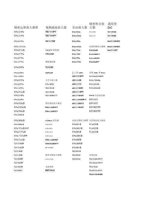
OPA333AID OPA2333AID OPA335AID
OPA2335AID
OPA365AID
OPA2365AID
OPA727AIDGKT OPA2727AID OPA4727AIPW OPA734AID TLV2460IP TLV2462IP
TLV2463IN TLV2465IN
TPS40200D
TPS40211DGQ
TUSB3410IVF TMP275AID ISO7221MD ISO7220MD ISO7241MD ISO7240MD CC1101RTK CC2500RTK CC2480A1RTC CC2520RHDT CC2591RGVT
电压反馈高速放大
器
SAR 型 ADC
TL431BILP JFET 高速放大器 OPA656U OPA657U
THS4631D
流水线型 ADC
TPS74401KTWT TPS75901KTTT TPS70302PWP TPS54K/SWIFT TPS54160DGQ TPS5430DDA TPS5450DDA TPS54350PWP TPS54550PWP
精密对数放大器数
LOG112AID
电流基准 REF200AU
电流反馈放大器馈 压控增益放大器益
OPA684ID
VCA820ID
OPA2684ID
VCA822ID
OPA691ID
VCA810ID
OPA2691ID
OPA695ID
OPA2695ID
OPA694ID
THS3001ID THS3091D
音频功放
时钟发生和分配器
TPS54331D
电压反向器
MSP430F4793IPZ
- 1、下载文档前请自行甄别文档内容的完整性,平台不提供额外的编辑、内容补充、找答案等附加服务。
- 2、"仅部分预览"的文档,不可在线预览部分如存在完整性等问题,可反馈申请退款(可完整预览的文档不适用该条件!)。
- 3、如文档侵犯您的权益,请联系客服反馈,我们会尽快为您处理(人工客服工作时间:9:00-18:30)。
FEATURES DESCRIPTIONAPPLICATIONSR FBI OUTGNDV DDVCSCLKSDIDAC8811SLAS411B–NOVEMBER2004–REVISED FEBRUARY2007 16-Bit,Serial Input Multiplying Digital-to-Analog Converter•±0.5LSB DNL The DAC8811multiplying digital-to-analog converter(DAC)is designed to operate from a single2.7-V to •16-Bit Monotonic5.5-V supply.•±1LSB INLThe applied external reference input voltage V REF •Low Noise:12nV/√Hzdetermines the full-scale output current.An internal •Low Power:I DD=2µAfeedback resistor(R FB)provides temperature •+2.7V to+5.5V Analog Power Supply tracking for the full-scale output when combined withan external I-to-V precision amplifier.•2mA Full-Scale Current±20%,with V REF=10V A serial data interface offers high-speed,three-wire •50-MHz Serial Interface microcontroller-compatible inputs using data-in(SDI),clock(CLK),and chip-select(CS).•0.5µs Settling Time•4-Quadrant Multiplying Reference On power-up,the DAC register is filled with zeroes,and the DAC output is at zero scale.•Reference Bandwidth:10MHzThe DAC8811is packaged in space-saving8-lead •±10V Reference InputSON and MSOP packages.•Reference Dynamics:-105THD•Tiny8-Lead3x3mm SON and3x5mmMSOP Packages•Industry-Standard Pin Configuration•Automatic Test Equipment•Instrumentation•Digitally Controlled Calibration•Industrial Control PLCsPlease be aware that an important notice concerning availability,standard warranty,and use in critical applications of TexasInstruments semiconductor products and disclaimers thereto appears at the end of this data sheet.PRODUCTION DATA information is current as of publication date.Copyright©2004–2007,Texas Instruments Incorporated Products conform to specifications per the terms of the TexasInstruments standard warranty.Production processing does notnecessarily include testing of all parameters.ABSOLUTE MAXIMUM RATINGSDAC8811SLAS411B–NOVEMBER 2004–REVISED FEBRUARY 2007This integrated circuit can be damaged by ESD.Texas Instruments recommends that all integrated circuits be handled with appropriate precautions.Failure to observe proper handling and installation procedures can cause damage.ESD damage can range from subtle performance degradation to complete device failure.Precision integrated circuits may be more susceptible to damage because very small parametric changes could cause the device not to meet its published specifications.PACKAGE/ORDERING INFORMATION (1)MINIMUM RELATIVE DIFFERENTIAL PACKAGE-SPECIFIED TRANSPORT ACCURACYNONLINEARITYLEADTEMPERATUREPACKAGE ORDERING MEDIA,PRODUCT (LSB)(LSB)(DESIGNATOR)RANGE MARKINGNUMBER QUANTITY DAC8811C ±1±1MSOP-8(DGK)-40°C to 85°C D11DAC8811ICDGKT Tape and Reel,250DAC8811C ±1±1MSOP-8(DGK)-40°C to 85°C D11DAC8811ICDGKR Tape and Reel,2500DAC8811C ±1±1SON-8(DRB)-40°C to 85°C D11DAC8811ICDRBT Tape and Reel,250DAC8811C ±1±1SON-8(DRB)-40°C to 85°C D11DAC8811ICDRBR Tape and Reel,2500DAC8811B ±2±1MSOP-8(DGK)-40°C to 85°C D11DAC8811IBDGKT Tape and Reel,250DAC8811B ±2±1MSOP-8(DGK)-40°C to 85°C D11DAC8811IBDGKR Tape and Reel,2500DAC8811B ±2±1SON-8(DRB)-40°C to 85°C D11DAC8811IBDRBT Tape and Reel,250DAC8811B±2±1SON-8(DRB)-40°C to 85°CD11DAC8811IBDRBRTape and Reel,2500(1)For the most current package and ordering information,see the Package Option Addendum at the end of this document,or see the TI Web site at .over operating free-air temperature range (unless otherwise noted)(1)DAC8811UNIT V DD to GND–0.3to 7V Digital input voltage to GND –0.3to +V DD +0.3V V (I OUT )to GND–0.3to +V DD +0.3V Operating temperature range –40to 105°C V REF ,R FB to GND –25to 25V Storage temperature range–65to 150°C Junction temperature range (T J max)125°C Power dissipation (T J max –T A )/R ΘJAW Thermal impedance,R ΘJA 55°C/W Lead temperature,soldering Vapor phase (60s)215°C Lead temperature,soldering Infrared (15s)220°C ESD rating,HBM 4000V ESD rating,CDM 1000V(1)Stresses above those listed under absolute maximum ratings may cause permanent damage to the device.Exposure to absolute maximum conditions for extended periods may affect device reliability.2Submit Documentation FeedbackELECTRICAL CHARACTERISTICSDAC8811 SLAS411B–NOVEMBER2004–REVISED FEBRUARY2007V DD =2.7V to5.5V;IOUT=Virtual GND,GND=0V;VREF=10V;TA=full operating temperature.All specifications-40°C to85°C,unless otherwise noted.DAC8811 PARAMETER CONDITIONS UNITSMIN TYP MAXSTATIC PERFORMANCEResolution16BitsRelative accuracy DAC8811C±1LSBRelative accuracy DAC8811B±2LSBDifferential nonlinearity±0.5±1LSBOutput leakage current Data=0000h,T A=25°C10nAOutput leakage current Data=0000h,T A=T MAX10nAFull-scale gain error All ones loaded to DAC register±1±4mVFull-scale tempco±3ppm/°C OUTPUT CHARACTERISTICS(1)Output current2mAOutput capacitance Code dependent50pF REFERENCE INPUT(1)V REF Range–1515VInput resistance5kΩInput capacitance5pF LOGIC INPUTS AND OUTPUT(1)V DD=2.7V0.6VV IL Input low voltageV DD=5V0.8VV DD=2.7V 2.1VV IH Input high voltageV DD=5V 2.4VI IL Input leakage current10µAC IL Input capacitance10pF INTERFACE TIMINGf CLK Clock input frequency50MHzt(CH)Clock pulse width high10nst(CL)Clock pulse width low10nst(CSS)CS to Clock setup time0nst(CSH)Clock to CS hold time10nst(DS)Data setup time5nst(DH)Data hold time10ns POWER REQUIREMENTSV DD 2.7 5.5VI DD(normal operation)Logic inputs=0V5µAV DD=4.5V to5.5V V IH=V DD and V IL=GND35µAV DD=2.7V to3.6V V IH=V DD and V IL=GND1 2.5µAAC CHARACTERISTICS(1)(2)To±0.1%of full-scale,Data=0000h to FFFFh to0000h0.3t s Output voltage settling timeµsTo±0.0015%of full-scale,Data=0000h to FFFFh to0.50000hBW–3dB Reference mutiplying BW V REF=5V PP,Data=FFFFh10MHz DAC glitch impulse V REF=0V to10V,Data=7FFFh to8000h to7FFFh2nV/sFeedthrough error V OUT/V REF Data=0000h,V REF=100mV RMS,f=100kHz–70dB(1)Specified by design and characterization;not production tested.(2)All ac characteristic tests are performed in a closed-loop system using the THS4011I-to-V converter amplifier.3Submit Documentation FeedbackPIN ASSIGNMENTSDRB PACKAGEDGK PACKAGER V R V DAC8811SLAS411B–NOVEMBER 2004–REVISED FEBRUARY 2007ELECTRICAL CHARACTERISTICS (continued)V DD =2.7V to 5.5V;I OUT =Virtual GND,GND =0V;V REF =10V;T A =full operating temperature.All specifications -40°C to 85°C,unless otherwise noted.DAC8811PARAMETER CONDITIONSUNITS MINTYP MAXDigital feedthrough CS =1and f CLK =1MHz2nV/s Total harmonic distortion V REF =5V PP ,Data =FFFFh,f =1kHz –105dB Output spot noise voltagef =1kHz,BW =1Hz12nV/√HzTable 1.TERMINAL FUNCTIONS4Submit Documentation FeedbackTYPICAL CHARACTERISTICS:V DD =5V1.00.80.60.40.20−0.2−0.4−0.6−0.8−1.0819216384245763276840960495125734465536I N L (L S B )Digital Input CodeT A =+25_C1.00.80.60.40.20−0.2−0.4−0.6−0.8−1.0D N L (L S B )T A =+25_C819216384245763276840960495125734465536Digital Input Code1.00.80.60.40.20−0.2−0.4−0.6−0.8−1.0T A =−40_CD N L (L S B )819216384245763276840960495125734465536Digital Input Code1.00.80.60.40.20−0.2−0.4−0.6−0.8−1.0T A =−40_CI N L (L S B )819216384245763276840960495125734465536Digital Input Code1.00.80.60.40.20−0.2−0.4−0.6−0.8−1.0I N L (L S B )T A =+85_C819216384245763276840960495125734465536Digital Input Code 1.00.80.60.40.20−0.2−0.4−0.6−0.8−1.0D N L (L S B )T A =+85_C819216384245763276840960495125734465536Digital Input CodeDAC8811SLAS411B–NOVEMBER 2004–REVISED FEBRUARY 2007At T A =25°C,+V DD =5V,unless otherwise noted.LINEARITY ERROR DIFFERENTIAL LINEARITY ERRORvs DIGITAL INPUT CODEvs DIGITAL INPUT CODEFigure 1.Figure 2.LINEARITY ERROR DIFFERENTIAL LINEARITY ERRORvs DIGITAL INPUT CODEvs DIGITAL INPUT CODEFigure 3.Figure 4.LINEARITY ERROR DIFFERENTIAL LINEARITY ERRORvs DIGITAL INPUT CODEvs DIGITAL INPUT CODEFigure 5.Figure 6.5Submit Documentation Feedback−−−−−−−−−−−−−−−−−−−A Digita l Codet t e n u a t i o n (d B )Bandwidth(Hz)1.61.41.21.00.80.60.40.2000.51.01.52.02.53.03.54.04.55.0Logic Input Voltage (V)S u p p l y C u r r e n t , I D D (m A )Time (0.1s/div)O u t p u t V o l t a g e (5V /d i v )Time (0.2µs/div)O u t p u t V o l t a g e (50m V /d i v )DAC8811SLAS411B–NOVEMBER 2004–REVISED FEBRUARY 2007TYPICAL CHARACTERISTICS:V DD =5V (continued)At T A =25°C,+V DD =5V,unless otherwise noted.SUPPLY CURRENT vs LOGIC INPUT VOLTAGEREFERENCE MULTIPLYING BANDWIDTHFigure 7.Figure 8.DAC GLITCHDAC SETTLING TIMEFigure 9.Figure 10.6Submit Documentation FeedbackTYPICAL CHARACTERISTICS:V DD =2.7V1.00.80.60.40.20−0.2−0.4−0.6−0.8−1.0I N L (L S B )T A =+25_C819216384245763276840960495125734465536Digital Input Code1.00.80.60.40.20−0.2−0.4−0.6−0.8−1.0D N L (L S B )T A =+25_C819216384245763276840960495125734465536Digital Input Code1.00.80.60.40.20−0.2−0.4−0.6−0.8−1.0T A =−40_CI N L (L S B )819216384245763276840960495125734465536Digital Input Code T A =−40_C1.00.80.60.40.20−0.2−0.4−0.6−0.8−1.0D N L (L S B )819216384245763276840960495125734465536Digital Input Code1.00.80.60.40.20−0.2−0.4−0.6−0.8−1.0I N L (L S B )T A =+85_C819216384245763276840960495125734465536Digital Input Code 1.00.80.60.40.20−0.2−0.4−0.6−0.8−1.0D N L (L S B )T A =+85_C819216384245763276840960495125734465536Digital Input CodeDAC8811SLAS411B–NOVEMBER 2004–REVISED FEBRUARY 2007At T A =25°C,+V DD =2.7V,unless otherwise noted.LINEARITY ERROR DIFFERENTIAL LINEARITY ERRORvs DIGITAL INPUT CODEvs DIGITAL INPUT CODEFigure 11.Figure 12.LINEARITY ERROR DIFFERENTIAL LINEARITY ERRORvs DIGITAL INPUT CODEvs DIGITAL INPUT CODEFigure 13.Figure 14.LINEARITY ERROR DIFFERENTIAL LINEARITY ERRORvs DIGITAL INPUT CODEvs DIGITAL INPUT CODEFigure 15.Figure 16.7Submit Documentation FeedbackTHEORY OF OPERATIONV REFGNDI OUTV OUT +*V REF CODE65536(1)V OV REFDAC8811SLAS411B–NOVEMBER 2004–REVISED FEBRUARY 2007The DAC8811is a single channel current output,16-bit digital-to-analog converter (DAC).The architecture,illustrated in Figure 17,is an R-2R ladder configuration with the three MSBs segmented.Each 2R leg of the ladder is to GND or the I OUT terminal.The I OUT terminal of the DAC is held at a virtual GND potential by the use of an external I/V converter op amp.The R-2R ladder is connected to an external reference input V REF that determines the DAC full-scale current.The R-2R ladder presents a code independent load impedance to the external reference of 5k Ω±25%.The external reference voltage can vary in a range of -15V to 15V,thus providing bipolar I OUT current operation.By using an external I/V converter and the DAC8811R FB resistor,output voltage ranges of -V REF to V REF can be generated.Figure 17.Equivalent R-2R DAC CircuitWhen using an external I/V converter and the DAC8811R FB resistor,the DAC output voltage is given by Equation 1:Each DAC code determines the 2R leg switch position to either GND or I OUT .Because the DAC outputimpedance as seen looking into the I OUT terminal changes versus code,the external I/V converter noise gain will also change.Because of this,the external I/V converter op amp must have a sufficiently low offset voltage such that the amplifier offset is not modulated by the DAC I OUT terminal impedance change.External op amps with large offset voltages can produce INL errors in the transfer function of the DAC8811due to offset modulation versus DAC code.For best linearity performance of the DAC8811,an op amp (OPA277)is recommended (Figure 18).This circuit allows V REF swinging from -10V to +10V.Figure 18.Voltage Output Configuration8Submit Documentation FeedbackSDI CLKCSAPPLICATION INFORMATIONStabilityCircuitV OUTPositive Voltage Output CircuitDAC8811SLAS411B–NOVEMBER 2004–REVISED FEBRUARY 2007THEORY OF OPERATION (continued)Figure 19.DAC8811Timing Diagram Table 2.Control Logic Truth Table (1)CLK CS Serial Shift Register DAC Register X H No effectLatched ↑+L Shift register data advanced one bit Latched X H No effectLatchedX ↑+Shift register data transferred to DAC registerNew data loaded from serial register(1)↑+Positive logic transition;X =Don't careTable 7.1.Serial Input Register Data Format,Data Loaded MSB FirstB15B0Bit (MSB)B14B13B12B11B10B9B8B7B6B5B4B3B2B1(LSB)DataD15D14D13D12D11D10D9D8D7D6D5D4D3D2D1D0For a current-to-voltage design (see Figure 20),the DAC8811current output (I OUT )and the connection with the inverting node of the op amp should be as short as possible and according to correct PCB layout design.For each code change there is a step function.If the GBP of the op amp is limited and parasitic capacitance is excessive at the inverting node then gain peaking is possible.Therefore,for circuit stability,a compensation capacitor C1(4pF to 20pF typ)can be added to the design,as shown in Figure 20.Figure 20.Gain Peaking Prevention Circuit With Compensation CapacitorAs Figure 21illustrates,in order to generate a positive voltage output,a negative reference is input to the design is suggested instead of using an inverting amp to invert the output due to tolerance errors of the resistor.For a negative reference,V OUT and GND of the reference are level-shifted to a virtual ground and a -2.5V input to the DAC8811with an op amp.9Submit Documentation FeedbackV OUTBipolar Output CircuitV OUT+ǒD32,768*1ǓV REF(2)V OUT10 k W10 k W+2.5V(+10V)Programmable Current Source CircuitI L +(R2)R3)ńR1R3VREFD(3)DAC8811SLAS411B–NOVEMBER2004–REVISED FEBRUARY2007APPLICATION INFORMATION(continued)Figure21.Positive Voltage Output CircuitThe DAC8811,as a2-quadrant multiplying DAC,can be used to generate a unipolar output.The polarity of the full-scale output I OUT is the inverse of the input reference voltage at V REF.Some applications require full4-quadrant multiplying capabilities or bipolar output swing.As shown in Figure22, external op amp U4is added as a summing amp and has a gain of2X that widens the output span4-quadrant multiplying circuit is implemented by using a 2.5-V offset of the reference voltage to bias U4. According to the circuit transfer equation given in Equation2,input data(D)from code0to full scale produces output voltages of V OUT=-2.5V to V OUT=+2.5V.External resistance mismatching is the significant error in Figure22.Figure22.Bipolar Output CircuitA DAC8811can be integrated into the circuit in Figure23to implement an improved Howland current pump for precise voltage to current conversions.flow and high voltage compliance are two features of the circuit.With a matched resistor network,the load current of the circuit is shown by Equation3:10Submit Documentation FeedbackZO+R1ȀR3(R1)R2)R1(R2Ȁ)R3Ȁ)*R1Ȁ(R2)R3)(4)V REFR244OUTCross-ReferenceDAC8811SLAS411B–NOVEMBER2004–REVISED FEBRUARY2007 APPLICATION INFORMATION(continued)The value of R3in the previous equation can be reduced to increase the output current drive of U3.U3can drive±20mA in both directions with voltage compliance limited up to15V by the U3voltage supply.Elimination of the circuit compensation capacitor C1in the circuit is not suggested as a result of the change in the output impedance Z O,according to Equation4:As shown in Equation4,with matched resistors,Z O is infinite and the circuit is optimum for use as a current source.resistors are used,Z O is positive or negative with negative output impedance being a potential cause of oscillation.Therefore,by incorporating C1into the circuit,possible oscillation problems are eliminated.The value of C1can be determined for critical applications;for most applications, however,a value of several pF is suggested.Figure23.Programmable Bidirectional Current Source CircuitThe DAC8811has an industry-standard pinout.Table3provides the cross-reference information.Table3.Cross-ReferenceSPECIFIEDTEMPERATURE PACKAGE PACKAGE CROSS-PRODUCT INL(LSB)DNL(LSB)RANGE DESCRIPTION OPTION REFERENCE PART DAC8811ICDGK±1±1-40°C to+85°C8-Lead MicroSOIC MSOP-8N/A DAC8811IBDGK±2±1-40°C to+85°C8-Lead MicroSOIC MSOP-8AD5543BRM DAC8811ICDRB±1±1-40°C to+85°C8-Lead Small Outline SON-8N/A DAC8811IBDRB±2±1-40°C to+85°C8-Lead Small Outline SON-8N/A N/A±2±1-40°C to+85°C8-Lead SOIC SOIC-8AD5543BR DAC8811SLAS411B–NOVEMBER 2004–REVISED FEBRUARY 2007Table 4.DAC8811Revision HistoryPACKAGING INFORMATIONOrderable Device Status(1)PackageType PackageDrawingPins PackageQtyEco Plan(2)Lead/Ball Finish MSL Peak Temp(3)DAC8811IBDGKR ACTIVE MSOP DGK82500Green(RoHS&no Sb/Br)CU NIPDAU Level-2-260C-1YEARDAC8811IBDGKRG4ACTIVE MSOP DGK82500Green(RoHS&no Sb/Br)CU NIPDAU Level-2-260C-1YEARDAC8811IBDGKT ACTIVE MSOP DGK8250Green(RoHS&no Sb/Br)CU NIPDAU Level-2-260C-1YEARDAC8811IBDGKTG4ACTIVE MSOP DGK8250Green(RoHS&no Sb/Br)CU NIPDAU Level-2-260C-1YEARDAC8811IBDRBR ACTIVE SON DRB83000Green(RoHS&no Sb/Br)CU NIPDAU Level-2-260C-1YEARDAC8811IBDRBRG4ACTIVE SON DRB83000Green(RoHS&no Sb/Br)CU NIPDAU Level-2-260C-1YEARDAC8811IBDRBT ACTIVE SON DRB8250Green(RoHS&no Sb/Br)CU NIPDAU Level-2-260C-1YEARDAC8811IBDRBTG4ACTIVE SON DRB8250Green(RoHS&no Sb/Br)CU NIPDAU Level-2-260C-1YEARDAC8811ICDGKR ACTIVE MSOP DGK82500Green(RoHS&no Sb/Br)CU NIPDAU Level-2-260C-1YEARDAC8811ICDGKRG4ACTIVE MSOP DGK82500Green(RoHS&no Sb/Br)CU NIPDAU Level-2-260C-1YEARDAC8811ICDGKT ACTIVE MSOP DGK8250Green(RoHS&no Sb/Br)CU NIPDAU Level-2-260C-1YEARDAC8811ICDGKTG4ACTIVE MSOP DGK8250Green(RoHS&no Sb/Br)CU NIPDAU Level-2-260C-1YEARDAC8811ICDRBR ACTIVE SON DRB83000Green(RoHS&no Sb/Br)CU NIPDAU Level-2-260C-1YEARDAC8811ICDRBRG4ACTIVE SON DRB83000Green(RoHS&no Sb/Br)CU NIPDAU Level-2-260C-1YEARDAC8811ICDRBT ACTIVE SON DRB8250Green(RoHS&no Sb/Br)CU NIPDAU Level-2-260C-1YEARDAC8811ICDRBTG4ACTIVE SON DRB8250Green(RoHS&no Sb/Br)CU NIPDAU Level-2-260C-1YEAR(1)The marketing status values are defined as follows:ACTIVE:Product device recommended for new designs.LIFEBUY:TI has announced that the device will be discontinued,and a lifetime-buy period is in effect.NRND:Not recommended for new designs.Device is in production to support existing customers,but TI does not recommend using this part in a new design.PREVIEW:Device has been announced but is not in production.Samples may or may not be available.OBSOLETE:TI has discontinued the production of the device.(2)Eco Plan-The planned eco-friendly classification:Pb-Free(RoHS),Pb-Free(RoHS Exempt),or Green(RoHS&no Sb/Br)-please check /productcontent for the latest availability information and additional product content details.TBD:The Pb-Free/Green conversion plan has not been defined.Pb-Free(RoHS):TI's terms"Lead-Free"or"Pb-Free"mean semiconductor products that are compatible with the current RoHS requirements for all6substances,including the requirement that lead not exceed0.1%by weight in homogeneous materials.Where designed to be soldered at high temperatures,TI Pb-Free products are suitable for use in specified lead-free processes.Pb-Free(RoHS Exempt):This component has a RoHS exemption for either1)lead-based flip-chip solder bumps used between the die and package,or2)lead-based die adhesive used between the die and leadframe.The component is otherwise considered Pb-Free(RoHS compatible)as defined above.Green(RoHS&no Sb/Br):TI defines"Green"to mean Pb-Free(RoHS compatible),and free of Bromine(Br)and Antimony(Sb)based flame retardants(Br or Sb do not exceed0.1%by weight in homogeneous material)(3)MSL,Peak Temp.--The Moisture Sensitivity Level rating according to the JEDEC industry standard classifications,and peak solder temperature.Important Information and Disclaimer:The information provided on this page represents TI's knowledge and belief as of the date that it is provided.TI bases its knowledge and belief on information provided by third parties,and makes no representation or warranty as to the accuracy of such information.Efforts are underway to better integrate information from third parties.TI has taken and continues to take reasonable steps to provide representative and accurate information but may not have conducted destructive testing or chemical analysis on incoming materials and chemicals.TI and TI suppliers consider certain information to be proprietary,and thus CAS numbers and other limited information may not be available for release.In no event shall TI's liability arising out of such information exceed the total purchase price of the TI part(s)at issue in this document sold by TI to Customer on an annual basis.TAPE AND REEL INFORMATION*All dimensions are nominal Device Package Type Package DrawingPinsSPQ Reel Diameter (mm)Reel Width W1(mm)A0(mm)B0(mm)K0(mm)P1(mm)W (mm)Pin1Quadrant DAC8811IBDGKR MSOPDGK 82500330.012.4 5.3 3.4 1.48.012.0Q1DAC8811IBDGKT MSOPDGK 8250330.012.4 5.3 3.4 1.48.012.0Q1DAC8811IBDRBR SONDRB 83000330.012.4 3.3 3.3 1.18.012.0Q2DAC8811IBDRBT SONDRB 8250330.012.4 3.3 3.3 1.18.012.0Q2DAC8811ICDGKR MSOPDGK 82500330.012.4 5.3 3.4 1.48.012.0Q1DAC8811ICDGKT MSOPDGK 8250330.012.4 5.3 3.4 1.48.012.0Q1DAC8811ICDRBR SONDRB 83000330.012.4 3.3 3.3 1.18.012.0Q2DAC8811ICDRBT SON DRB 8250330.012.4 3.3 3.3 1.18.012.0Q2*All dimensions are nominalDevice Package Type Package Drawing Pins SPQ Length(mm)Width(mm)Height(mm) DAC8811IBDGKR MSOP DGK82500346.0346.029.0 DAC8811IBDGKT MSOP DGK8250346.0346.029.0 DAC8811IBDRBR SON DRB83000340.5333.020.6 DAC8811IBDRBT SON DRB8250340.5333.020.6 DAC8811ICDGKR MSOP DGK82500346.0346.029.0 DAC8811ICDGKT MSOP DGK8250346.0346.029.0 DAC8811ICDRBR SON DRB83000340.5333.020.6DAC8811ICDRBT SON DRB8250340.5333.020.6IMPORTANT NOTICETexas Instruments Incorporated and its subsidiaries(TI)reserve the right to make corrections,modifications,enhancements,improvements, and other changes to its products and services at any time and to discontinue any product or service without notice.Customers should obtain the latest relevant information before placing orders and should verify that such information is current and complete.All products are sold subject to TI’s terms and conditions of sale supplied at the time of order acknowledgment.TI warrants performance of its hardware products to the specifications applicable at the time of sale in accordance with TI’s standard warranty.Testing and other quality control techniques are used to the extent TI deems necessary to support this warranty.Except where mandated by government requirements,testing of all parameters of each product is not necessarily performed.TI assumes no liability for applications assistance or customer product design.Customers are responsible for their products and applications using TI components.To minimize the risks associated with customer products and applications,customers should provide adequate design and operating safeguards.TI does not warrant or represent that any license,either express or implied,is granted under any TI patent right,copyright,mask work right, or other TI intellectual property right relating to any combination,machine,or process in which TI products or services are rmation published by TI regarding third-party products or services does not constitute a license from TI to use such products or services or a warranty or endorsement e of such information may require a license from a third party under the patents or other intellectual property of the third party,or a license from TI under the patents or other intellectual property of TI.Reproduction of TI information in TI data books or data sheets is permissible only if reproduction is without alteration and is accompanied by all associated warranties,conditions,limitations,and notices.Reproduction of this information with alteration is an unfair and deceptive business practice.TI is not responsible or liable for such altered rmation of third parties may be subject to additional restrictions.Resale of TI products or services with statements different from or beyond the parameters stated by TI for that product or service voids all express and any implied warranties for the associated TI product or service and is an unfair and deceptive business practice.TI is not responsible or liable for any such statements.TI products are not authorized for use in safety-critical applications(such as life support)where a failure of the TI product would reasonably be expected to cause severe personal injury or death,unless officers of the parties have executed an agreement specifically governing such use.Buyers represent that they have all necessary expertise in the safety and regulatory ramifications of their applications,and acknowledge and agree that they are solely responsible for all legal,regulatory and safety-related requirements concerning their products and any use of TI products in such safety-critical applications,notwithstanding any applications-related information or support that may be provided by TI.Further,Buyers must fully indemnify TI and its representatives against any damages arising out of the use of TI products in such safety-critical applications.TI products are neither designed nor intended for use in military/aerospace applications or environments unless the TI products are specifically designated by TI as military-grade or"enhanced plastic."Only products designated by TI as military-grade meet military specifications.Buyers acknowledge and agree that any such use of TI products which TI has not designated as military-grade is solely at the Buyer's risk,and that they are solely responsible for compliance with all legal and regulatory requirements in connection with such use. TI products are neither designed nor intended for use in automotive applications or environments unless the specific TI products are designated by TI as compliant with ISO/TS16949requirements.Buyers acknowledge and agree that,if they use any non-designated products in automotive applications,TI will not be responsible for any failure to meet such requirements.Following are URLs where you can obtain information on other Texas Instruments products and application solutions:Products ApplicationsAmplifiers Audio /audioData Converters Automotive /automotiveDLP®Products Communications and /communicationsTelecomDSP Computers and /computersPeripheralsClocks and Timers /clocks Consumer Electronics /consumer-appsInterface Energy /energyLogic Industrial /industrialPower Mgmt Medical /medicalMicrocontrollers Security /securityRFID Space,Avionics&/space-avionics-defenseDefenseRF/IF and ZigBee®Solutions /lprf Video and Imaging /videoWireless /wireless-appsMailing Address:Texas Instruments,Post Office Box655303,Dallas,Texas75265Copyright©2010,Texas Instruments Incorporated。