HCF40208BEY中文资料
HEF4020BT资料

HEF4020B14-stage binary counterRev. 04 — 4 December 2008Product data sheet1.General descriptionThe HEF4020B is a 14-stage binary counter with a clock input (CP), an overridingasynchronous master reset input (MR) and twelve fully buffered outputs (Q0, and Q3 toQ13).The counter advances on the HIGH to LOW transition of CP.A HIGH on MR clearsall counter stages and forces all outputs LOW, independent of the state of CP. Eachcounter stage is a static toggle flip-flop. A feature of the device is its high speed(typ.35MHz at V DD=15V).It operates over a recommended V DD power supply range of3V to15V referenced to V SS(usually ground). Unused inputs must be connected to V DD, V SS, or another input. It isalso suitable for use over the full industrial (−40°C to +85°C) temperature range.2.FeaturesI High speed operationI Fully static operationI 5 V, 10 V, and 15 V parametric ratingsI Standardized symmetrical output characteristicsI Operates across the full industrial temperature range−40°C to +85°CI Complies with JEDEC standard JESD 13-BI ESD protection:N HBM JESD22-A114E exceeds 2000VN MM JESD22-A115-A exceeds 200V3.ApplicationsI Industrial4.Ordering informationTable 1.Ordering informationAll types operate from−40°C to +85°C.Type number PackageName Description Version HEF4020BP DIP16plastic dual in-line package; 16-leads (300 mil)SOT38-4 HEF4020BT SO16plastic small outline package; 16 leads; body width 3.9mm SOT109-15.Functional diagramFig 1.Functional diagram001aad72214-STAGE COUNTER9Q07Q35Q44Q56Q613Q712Q814Q915Q101Q112Q123Q131011T C D MRCP Fig 2.Logic symbol Fig 3.IEC Logic symbol001aad723Q0911MR10CPQ37Q45Q54Q66Q713Q812Q914Q1015Q111Q122Q133001aad724911CT+ 10CTR14CT75461312141512133Fig 4.Logic diagram001aad725CPMRFF 0QT RDQ0Q FF 2QT RDQFF 7QT RDQ7Q FF 9QT RDQ9QFF 1QT RDQFF 8QT RDQ8QFF 10QT RDQ10QFF 11QT RDQ11QFF 12QT RDQ12QFF 13QT RDQ13QFF 3QT RDQ3QFF 4QT RDQ4Q FF 5QT RDQ5QFF 6QT RDQ6Q6.Pinning information6.1Pinning6.2Pin description7.Functional description[1]H = HIGH voltage level; L = LOW voltage level; X = don’t care;↑ = positive-going transition;↓ = negative-going transition.Fig 5.Pin configurationHEF4020BQ11V DD Q12Q10Q13Q9Q5Q7Q4Q8Q6MR Q3CP V SSQ0001aaj10112345678109121114131615Table 2.Pin descriptionSymbol PinDescriptionQ3 to Q137, 5, 4, 6, 13, 12, 14, 15, 1, 2, 3parallel output (Q3 to Q13)V SS 8ground supply voltage Q09parallel outputCP 10clock input (HIGH-to-LOW edge triggered)MR 11master reset input (active HIGH)V DD16supply voltageTable 3.Functional table [1]Input OutputCPMR Q0, Q3 to Q13↑L no change ↓L count XHL8.Limiting values[1]For DIP16 package: P tot derates linearly with 12 mW/K above 70°C.[2]For SO16 package: P tot derates linearly with 8 mW/K above 70°C.Fig 6.Timing diagram001aad7261248163264128256512102420484096CP input MR inputQ0Q3Q4Q5Q6Q7Q8Q9Q10Q11819216384Q12Q13Table 4.Limiting valuesIn accordance with the Absolute Maximum Rating System (IEC 60134).Symbol Parameter ConditionsMin Max Unit V DD supply voltage −0.5+18V I IK input clamping current V I <0.5V or V I >V DD + 0.5 V -±10mA V I input voltage−0.5V DD + 0.5V I OK output clamping current V O <0.5V or V O >V DD +0.5V-±10mA I I/O input/output current -±10mA I DD supply current -50mA T stg storage temperature −65+150°C T amb ambient temperature −40+85°C P tottotal power dissipationT amb −40°C to +85°C DIP16 package [1]-750mW SO16 package[2]-500mW Ppower dissipation per output-100mW9.Recommended operating conditionsTable 5.Recommended operating conditionsSymbol Parameter Conditions Min Typ Max UnitV DD supply voltage3-15VV I input voltage0-V DD VT amb ambient temperature in free air−40-+85°C∆t/∆V input transition rise and fall rate V DD = 5 V-- 3.75ns/VV DD = 10 V--0.5ns/VV DD = 15 V--0.08ns/V 10.Static characteristicsTable 6.Static characteristicsV SS = 0 V; V I = V SS or V DD; unless otherwise specified.Symbol Parameter Conditions V DD T amb =−40°C T amb = 25°C T amb = 85°C UnitMin Max Min Max Min MaxV IH HIGH-level input voltage|I O| < 1µA 5 V 3.5- 3.5- 3.5-V10 V7.0-7.0-7.0-V15 V11.0-11.0-11.0-VV IL LOW-level input voltage|I O| < 1µA 5 V- 1.5- 1.5- 1.5V10 V- 3.0- 3.0- 3.0V15 V- 4.0- 4.0- 4.0VV OH HIGH-level output voltage|I O| < 1µA 5 V 4.95- 4.95- 4.95-V10 V9.95-9.95-9.95-V15 V14.95-14.95-14.95-VV OL LOW-level output voltage|I O| < 1µA 5 V-0.05-0.05-0.05V10 V-0.05-0.05-0.05V15 V-0.05-0.05-0.05VI OH HIGH-level output current V O = 2.5 V 5 V−1.7-−1.4-−1.1-mAV O = 4.6 V 5 V−0.52-−0.44-−0.36-mAV O = 9.5 V10 V−1.3-−1.1-−0.9-mAV O = 13.5 V15 V−3.6-−3.0-−2.4-mA I OL LOW-level output current V O = 0.4 V 5 V0.52-0.44-0.36-mAV O = 0.5 V10 V 1.3- 1.1-0.9-mAV O = 1.5 V15 V 3.6- 3.0- 2.4-mA I I input leakage current15 V-±0.3-±0.3-±1.0µAI DD supply current I O = 0A 5 V-20-20-150µA10 V-40-40-300µA15 V-80-80-600µAC I input capacitance----7.5--pF11.Dynamic characteristics[1]The typical values of the propagation delay and transition times are calculated from the extrapolation formulas shown (C L in pF).Table 7.Dynamic characteristicsV SS = 0 V; T amb = 25°C; for test circuit see Figure 8.Symbol Parameter Conditions V DD Extrapolation formula [1]Min Typ Max Unit t PHLHIGH to LOW propagation delayCP to Q0;see Figure 75 V 78 ns + (0.55 ns/pF) C L -105210ns 10 V 34 ns + (0.23 ns/pF) C L -4590ns 15 V22 ns + (0.16 ns/pF) C L -3065ns Qn to Qn +15 V 53 ns + (0.55 ns/pF) C L -80160ns 10 V 19 ns + (0.23 ns/pF) C L -3060ns 15 V12 ns + (0.16 ns/pF) C L -2040ns MR to Qn;see Figure 75 V 153 ns + (0.55 ns/pF) C L -180360ns 10 V 79 ns + (0.23 ns/pF) C L -90180ns 15 V62 ns + (0.16 ns/pF) C L -70140ns t PLHLOW to HIGH propagation delayCP to Q0;see Figure 75 V 78 ns + (0.55 ns/pF) C L -105210ns 10 V 39 ns + (0.23 ns/pF) C L -5095ns 15 V27 ns + (0.16 ns/pF) C L -3570ns Qn to Qn +15 V 43 ns + (0.55 ns/pF) C L -70140ns 10 V 14 ns + (0.23 ns/pF) C L -2550ns 15 V12 ns + (0.16 ns/pF) C L -2040ns t ttransition timesee Figure 75 V 10 ns + (1.00 ns/pF) C L -60120ns 10 V 9 ns + (0.42 ns/pF) C L -3060ns 15 V6 ns + (0.28 ns/pF) C L-2040ns t Wpulse widthCP = HIGH;minimum width;see Figure 7 5 V 5025-ns 10 V 2515-ns 15 V 2010-ns MR = HIGH;minimum width;see Figure 75 V 13065-ns 10 V 9550-ns 15 V 9045-ns t recrecovery timeMR input;see Figure 75 V 11560-ns 10 V 6535-ns 15 V5525-ns f maxmaximum frequencysee Figure 75 V 510-MHz 10 V 1325-MHz 15 V1835-MHz12.WaveformsTable 8.Dynamic power dissipation P DP D can be calculated from the formulas shown. V SS = 0 V; t r = t f ≤ 20 ns; T amb = 25°C.Symbol Parameter V DD Typical formula for P D (µW)where:P Ddynamic power dissipation5V P D = 600× f i +Σ(f o × C L )× V DD 2f i = input frequency in MHz,f o = output frequency in MHz,C L = output load capacitance in pF ,V DD = supply voltage in V ,Σ(C L × f o ) = sum of the outputs.10V P D = 2800× f i +Σ(f o × C L )× V DD 215VP D = 8200× f i +Σ(f o × C L )× V DD 2Measurement points are given in Table 9.Fig 7.Propagation delays,minimum pulse widths,transition and recovery times and maximum clock frequency MR INPUTV IQ0 or Qn OUTPUTt Wt PHLt rec 1/f maxV MV MV M001aae591t PLH t Wt tt tt PHLCP INPUTV IV OHV OLV SS V SSTable 9.Measurement pointsSupply voltage Input Output V DDV M V M 5 V to 15 V0.5V DD0.5V DDTest data is given in T able 10.Definitions for test circuit:DUT = Device Under Test.C L =load capacitance including jig and probe capacitance.R T =termination resistance should be equal to the output impedance Z o of the pulse generator.Fig 8.Test circuitV DDV IV O001aag182DUTC LR TGTable 10.Test dataSupply voltage Input Load V DD V I t r, t f C L5V to 15V V SS or V DD≤20ns50 pF13.Package outlineFig 9.Package outline SOT38-4 (DIP16)REFERENCESOUTLINE VERSION EUROPEAN PROJECTIONISSUE DATE IECJEDECJEITASOT38-495-01-1403-02-13M Hc(e )1M EALs e a t i n g p l a n eA 1w Mb 1b 2eDA 2Z16198Epin 1 indexb0510 mmscaleNote1. Plastic or metal protrusions of 0.25 mm (0.01 inch) maximum per side are not included.UNIT Amax.12b 1(1)(1)(1)b 2c D E e M Z H L mm DIMENSIONS (inch dimensions are derived from the original mm dimensions)A min. A max.b max.w M E e 11.731.300.530.380.360.2319.5018.55 6.486.20 3.603.050.2542.547.628.257.8010.08.30.764.20.51 3.2inches0.0680.0510.0210.0150.0140.0091.250.850.0490.0330.770.730.260.240.140.120.010.10.30.320.310.390.330.030.170.020.13DIP16: plastic dual in-line package; 16 leads (300 mil)SOT38-4Fig 10.Package outline SOT109-1 (SO16)Xw MθAA 1A 2b pD H EL pQdetail XE Z ecL v M A(A )3A89116ypin 1 indexUNIT Amax.A 1A 2A 3b p c D (1)E (1)(1)e H E L L p Q Z y w v θREFERENCESOUTLINE VERSION EUROPEAN PROJECTIONISSUE DATE IEC JEDEC JEITAmm inches1.750.250.101.451.250.250.490.360.250.1910.09.84.03.8 1.27 6.25.80.70.60.70.380oo 0.250.1DIMENSIONS (inch dimensions are derived from the original mm dimensions)Note1. Plastic or metal protrusions of 0.15 mm (0.006 inch) maximum per side are not included.1.00.4 SOT109-199-12-2703-02-19076E07MS-0120.0690.0100.0040.0570.0490.010.0190.0140.01000.00750.390.380.160.150.051.050.0410.2440.2280.0280.0200.0280.0120.010.250.010.0040.0390.0160 2.5 5 mmscaleSO16: plastic small outline package; 16 leads; body width 3.9 mm SOT109-114.Abbreviations15.Revision historyTable 11.AbbreviationsAcronym Description DUT Device Under Test ESD ElectroStatic Discharge HBM Human Body Model MMMachine ModelTable 12.Revision historyDocument ID Release date Data sheet status Change notice Supersedes HEF4020B_420081204Product data sheet-HEF4020B_CNV_3Modifications:•The format of this data sheet has been redesigned to comply with the new identity guidelines of NXP Semiconductors.•Legal texts have been adapted to the new company name where appropriate.•Parallel output pins renamed Q0 to Q13 throughout.•T emperature statement added to Section 1 “General description”.•Section 2 “Features” added.•Table 1 “Ordering information” restructured.•Package version SOT38-1 changed to SOT38-4 in Section 4, and Figure 9. Package SOT74 removed from Section 4.•Figure 1 “Functional diagram”,Figure 4 “Logic diagram”,Figure 5 “Pin configuration”,Figure 7 “Propagation delays, minimum pulse widths, transition and recovery times and maximum clock frequency” and Figure 6 “Timing diagram” changed for pin name changes.•Figure 2 “Logic symbol” and Figure 3 “IEC Logic symbol” added.•Table 2 “Pin description” edited for pin name changes.•Section 7 “Functional description” added.•Section 8 “Limiting values” and Section 10 “Static characteristics” added, taken from the HE4000B Family Specifications data sheet.•t RMR , t WCPH and t WMRH changed to t rec and t W for Table 7 “Dynamic characteristics” and Figure 7 “Propagation delays, minimum pulse widths, transition and recovery times and maximum clock frequency”.•50% replaced by V M for Figure 7 “Propagation delays, minimum pulse widths, transition and recovery times and maximum clock frequency”.•Table 9 “Measurement points”,Figure 8 “T est circuit” and Table 10 “T est data” added.HEF4020B_CNV_319950101Product specification -HEF4020B_CNV_2HEF4020B_CNV_219950101Product specification--16.Legal information16.1Data sheet status[1]Please consult the most recently issued document before initiating or completing a design.[2]The term ‘short data sheet’ is explained in section “Definitions”.[3]The product status of device(s)described in this document may have changed since this document was published and may differ in case of multiple devices.The latest product status information is available on the Internet at URL .16.2DefinitionsDraft —The document is a draft version only. The content is still under internal review and subject to formal approval, which may result in modifications or additions. NXP Semiconductors does not give any representations or warranties as to the accuracy or completeness ofinformation included herein and shall have no liability for the consequences of use of such information.Short data sheet —A short data sheet is an extract from a full data sheet with the same product type number(s)and title.A short data sheet is intended for quick reference only and should not be relied upon to contain detailed and full information. For detailed and full information see the relevant full data sheet, which is available on request via the local NXP Semiconductors sales office. In case of any inconsistency or conflict with the short data sheet, the full data sheet shall prevail.16.3DisclaimersGeneral —Information in this document is believed to be accurate andreliable.However,NXP Semiconductors does not give any representations or warranties,expressed or implied,as to the accuracy or completeness of such information and shall have no liability for the consequences of use of such information.Right to make changes —NXP Semiconductors reserves the right to make changes to information published in this document, including withoutlimitation specifications and product descriptions, at any time and without notice.This document supersedes and replaces all information supplied prior to the publication hereof.Suitability for use —NXP Semiconductors products are not designed,authorized or warranted to be suitable for use in medical, military, aircraft,space or life support equipment, nor in applications where failure ormalfunction of a NXP Semiconductors product can reasonably be expected to result in personal injury, death or severe property or environmental damage.NXP Semiconductors accepts no liability for inclusion and/or use of NXP Semiconductors products in such equipment or applications and therefore such inclusion and/or use is at the customer’s own risk.Applications —Applications that are described herein for any of these products are for illustrative purposes only. NXP Semiconductors makes no representation or warranty that such applications will be suitable for the specified use without further testing or modification.Limiting values —Stress above one or more limiting values (as defined in the Absolute Maximum Ratings System of IEC 60134)may cause permanent damage to the device.Limiting values are stress ratings only and operation of the device at these or any other conditions above those given in theCharacteristics sections of this document is not implied. Exposure to limiting values for extended periods may affect device reliability.Terms and conditions of sale —NXP Semiconductors products are sold subject to the general terms and conditions of commercial sale,as published at /profile/terms , including those pertaining to warranty,intellectual property rights infringement and limitation of liability, unless explicitly otherwise agreed to in writing by NXP Semiconductors. In case of any inconsistency or conflict between information in this document and such terms and conditions, the latter will prevail.No offer to sell or license —Nothing in this document may be interpreted or construed as an offer to sell products that is open for acceptance or the grant,conveyance or implication of any license under any copyrights,patents or other industrial or intellectual property rights.16.4TrademarksNotice:All referenced brands,product names,service names and trademarks are the property of their respective owners.17.Contact informationFor more information, please visit:For sales office addresses, please send an email to:salesaddresses@Document status [1][2]Product status [3]DefinitionObjective [short] data sheet Development This document contains data from the objective specification for product development.Preliminary [short] data sheet Qualification This document contains data from the preliminary specification.Product [short] data sheetProductionThis document contains the product specification.18.Contents1General description. . . . . . . . . . . . . . . . . . . . . . 12Features . . . . . . . . . . . . . . . . . . . . . . . . . . . . . . . 13Applications. . . . . . . . . . . . . . . . . . . . . . . . . . . . 14Ordering information. . . . . . . . . . . . . . . . . . . . . 15Functional diagram . . . . . . . . . . . . . . . . . . . . . . 26Pinning information. . . . . . . . . . . . . . . . . . . . . . 36.1Pinning . . . . . . . . . . . . . . . . . . . . . . . . . . . . . . . 36.2Pin description . . . . . . . . . . . . . . . . . . . . . . . . . 37Functional description . . . . . . . . . . . . . . . . . . . 38Limiting values. . . . . . . . . . . . . . . . . . . . . . . . . . 49Recommended operating conditions. . . . . . . . 510Static characteristics. . . . . . . . . . . . . . . . . . . . . 511Dynamic characteristics . . . . . . . . . . . . . . . . . . 612Waveforms . . . . . . . . . . . . . . . . . . . . . . . . . . . . . 713Package outline . . . . . . . . . . . . . . . . . . . . . . . . . 914Abbreviations. . . . . . . . . . . . . . . . . . . . . . . . . . 1115Revision history. . . . . . . . . . . . . . . . . . . . . . . . 1116Legal information. . . . . . . . . . . . . . . . . . . . . . . 1216.1Data sheet status . . . . . . . . . . . . . . . . . . . . . . 1216.2Definitions. . . . . . . . . . . . . . . . . . . . . . . . . . . . 1216.3Disclaimers. . . . . . . . . . . . . . . . . . . . . . . . . . . 1216.4T rademarks. . . . . . . . . . . . . . . . . . . . . . . . . . . 1217Contact information. . . . . . . . . . . . . . . . . . . . . 1218Contents. . . . . . . . . . . . . . . . . . . . . . . . . . . . . . 13Please be aware that important notices concerning this document and the product(s)described herein, have been included in section ‘Legal information’.© NXP B.V.2008.All rights reserved.For more information, please visit: For sales office addresses, please send an email to: salesaddresses@Date of release: 4 December 2008。
HCC40108B
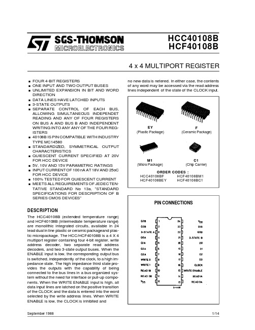
HCC40108B HCF40108BSeptembe r 19884x 4MULTIPORT REGISTEREY(Plastic Package)DESCRIPTIONORDER CODES :HCC40108BF HCF40108BM1HCF40108BEY HCF40108BC1F(Ceramic Package)M1(Micro Package)C1(Chip Carrier)PIN CONNECTIONSThe HCC40108B (extended temperature range)and HCF40108B (intermediate temperature range)are monolithic integrated circuits,available in 24lead dual in line plastic or ceramic packageand plas-tic micropackage.The HCC/HCF40108B is a 4X 4multiport register containing four 4-bit register,write address decoder,two separate read address decoder s,and two 3-state output buses.When the ENABLE input is low,the corresponding output bus is switched,independently of the clock,to a high im-pedance state.The high impedance third state pro-vides the outputs with the capability of being connected to the bus lines in a bus organized sys-tem without the need for interface or pull-up compo-nents.When the WRITE ENABLE input is high,all data input lines are latched on the positive transition of the CLOCK and the data is entered into the word selected by the write address lines.When WRITE ENABLE is low,the CLOCK is inhibited and.FOUR 4-BIT REGISTERS.ONE INPUT AND TWO OUTPUT BUSES.UNLIMITED EXPANSION IN BIT AND WORD DIRECTION.DATA LINES HAVE LATCHED INPUTS .3-STATE OUTPUTS.SEPARATE CONTROL OF EACH BUS,ALLOWING SIMULTANEOUS INDEPENDET READING AND ANY OF FOUR REGISTERS ON BUS A AND BUS B AND INDEPENDENT WRITING INTO ANY ANY OF THE FOUR REG-ISTERS.40108B IS PIN COMPATIBLE WITH INDUSTRY TYPE MC14580.STANDARDIZED,SYMMETRICAL OUTPUT CHARACTERISTICS.QUIESCENT CURRENT SPECIFIED AT 20V FOR HCC DEVICE.5V,10V AND 15V PARAMETRIC RATINGS .INPUT CURRENTOF 100nA AT 18V AND 25oC FOR HCC DEVICE.100%TESTED FOR QUIESCENT CURRENT .MEETS ALL REQUIREMENTS OF JEDECTEN-TATIVE STANDARD No 13a,”STANDARD SPECIFICATIONS FOR DESCRIPTION OF B SERIES CMOS DEVICES”no new data is netered.In either case,the contents of any word may be accessed via the read address lines indepe ndent of the state of the CLOCK input.1/14HCC/HCF40108 FUNCTIONAL DIAGRAMLOGIC DIAGRAM2/14ABSOLUTE MAXIMUM RATINGSymbol Parameter Value UnitV DD*Supply Voltage:HCC TypesHCF Types -0.5to+20-0.5to+18VVV i Input Voltage-0.5to V DD+0.5V I I DC Input Current(any one input)±10mAP tot Total Power Dissipation(per package)Dissipation per Output Transistorfor Top=Full Package Temperature Range 200100mWmWT op Operating Temperature:HCC TypesHCF Types -55to+125-40to+85o Co CT stg Storage Temperature-65to+150o C Stresses abov e those listedunder”Absolute Maximum Ratings”may cau se permanen t damage to thedevice.This is a stress ratingonly and functional opera tion of the device at thes e or any other cond itions above those indicated in the ope rational sections of this specification is not implied.Exposure to absolute maximum rating conditions for external periods may affect device reliability.*All voltage values are referred to V SS pin voltage.RECOMMENDED OPERATING CONDITIONSSymbol Parameter Value UnitV DD Supply Voltage:HCC TypesHCF Types 3to183to15VVV I Input Voltage0to V DD VT op Operating Temperature:HCC TypesHCF Types -55to+125-40to+85o Co CTRUTH TABLECLOCKWriteEnableWrite1Write2Read1ARead0ARead1BRead0BEnableAEnableBD n Q nA Q nB1S1S2S1S2S1S211111 1S1S2S1S2S1S210000X X X X X X X X0X Z Z Z100011011D n toword0Word1OutWord2Out000011011Word0notalteredWord1OutWord2OutX X X X10011X X Word2OutWord1OutX X X X X X X11X NC NC1=HIGH LEVEL,0=LOW LEVEL,X=DON’T CARE,Z=HIGH IMPEDANCES1and S2refer to input strates of either1or0HCC/HCF401083/14HCC/HCF40108 SCHEMATIC DIAGRAM4/14STATIC ELECTRICAL CHARACTERISTICS (over recommended operating conditions)Symbol Parameter Test ConditiosValue UnitV I(V)V O (V)|I O |(µA)V DD (V)T LOW *25o C T HIGH *Min.Max.Min.Typ.Max.Min.Max.I LQuiescent CurrentHCC Types0/5550.045150µA0/1010100.04103000/1515200.04206000/20201000.081003000HCFTypes 0/55200.04201500/1010400.04403000/1515800.0480600V OHOutput High Voltage 0/5<15 4.95 4.95 4.95V0/10<1109.959.959.950/15<11514.9514.9514.95V OLOutput Low Voltage 5/0<150.050.050.05V10/0<1100.050.050.0515/0<1150.050.050.05V IHInput High Voltage 0.5/4.5<15 3.5 3.53.5V1/9<1107771.5/13.5<115111111V ILInput Low Voltage 4.5/0.5<15 1.5 1.5 1.5V9/1<11033313.5/1.5<115444I OHOutput Drive CurrentHCC Types0/5 2.55-2-1.6-3.2-1.15mA0/5 4.65-0.64-0.51-1-0.360/109.510-1.6-1.3-2.6-0.90/1513.515-4.2-3.4-6.8-2.4HCF Types0/5 2.55-1.53-1.36-3.2-1.10/5 4.65-0.52-0.44-1-0.360/109.510-1.3-1.1-2.6-0.90/1513.515-3.6-3.0-6.8-2.4I OLOutput Sink CurrentHCC Types 0/50.450.640.5110.36mA0/100.510 1.6 1.3 2.60.90/15 1.515 4.2 3.4 6.8 2.4HCF Types0/50.450.520.4410.360/100.510 1.3 1.1 2.60.90/151.515 3.63.06.8 2.4I IH ,I ILInput Leakage Current HCCTypes 0/18Any Input18±0.1±10-5±0.1±1µAHCFTypes 0/1515±0.3±10-5±0.3±1I OH ,I OL**3-Sate Output Leakage CurrentHCCTypes 0/180/1818±0.4±10-4±0.4±12µAHCFTypes0/150/1515±1.0±10-4±1.0±7.5C I Input CapacitanceAny Input57.5pF*T LOW =-55oC for HCC device:-40oC for HCF device.*T HIGH =+125o C for HCC device:+85o C for HCF device.The Noise Margin for both ”1”and ”0”level is:1V min.with V DD =5V,2V min.with V DD =10V,2.5V min.withV DD =15V **Forced output disableHCC/HCF401085/14DYNAMIC ELECTRICAL CHARACTERISTICS (T amb =25o C,C L =50pF,R L =200K Ω,typical temperature coefficent for all V DD values is 03%/oC,all input rise and fall times=20ns)Symbol ParameterTest ConditionsValue UnitV DD (V)Min.Typ.Max.t PLH t PHLPropagation Delay Time Clock or Write Enable to Q 5360720ns1014028015100200Propagation Delay Time Read or Write Address to Q5300600101202401585170t PZH t PHZ 3-State Disable Delay Time5100200ns1050100154080t PZL t PLZ 3-State Display Delay Time5130260ns10601201550100t TLH t THL Output Transition Time5100200ns1050100154080t setupSetup TimeData to Clock t s(D)50-95ns100-35150-20Setup TimeWrite Enable to Clock t s(WE)52501251010050157035Setup TimeWrite Address to Clock t s(WA)52501251010050157035t r ,t s Clock Rise and Fall Time515µs105155t holdHold TimeData to Clock t s(D)5220110ns1010050158040Hold TimeWrite Enable to Clock t s(WE)52701351013065158040Hold TimeWrite Address to Clock t s(WA)53301651014070159045t WClock Pulse WidthClock or Write Enable t W(CL)5350175ns1013065159045Clock Pulse Width Write Address t W(WA)53001501015075159045f CL Maximum Clock Input Frequency5 1.53MHz10 3.57154.59HCC/HCF401086/14Output Low(sink)Current Characteristics Typical Propagation Delay Time vs Load Capa-citance(CL or WE to Q)Typical Dynamic Power Dissipation vs Input Fre-quency Output High(source)Current Characteristics Typical Transition Time vs Load CapacitanceHCC/HCF401087/14HCC/HCF40108TIMING DIAGRAMTEST CIRCUITSOutput Enable Delay Times and Waveforms 8/14HCC/HCF40108 Power Dissipation and WaveformsQuiescent Device Current.Noise Immunity.Input Leakage Current.9/14HCC/HCF40108Plastic DIP24(0.25)MECHANICAL DATAmm inch DIM.MIN.TYP.MAX.MIN.TYP.MAX.a10.630.025b0.450.018b10.230.310.0090.012 b2 1.270.050D32.2 1.268 E15.216.680.5980.657e 2.540.100e327.94 1.100F14.10.555I 4.4450.175L 3.30.130P043A 10/14Ceramic DIP24MECHANICAL DATAmm inchDIM.MIN.TYP.MAX.MIN.TYP.MAX. A32.3 1.272 B13.0513.360.5140.526 C 3.9 5.080.1540.200 D30.118E0.5 1.780.0200.070 e327.94 1.100F 2.29 2.790.0900.110 G0.40.550.0160.022 I 1.17 1.520.0460.060 L0.220.310.0090.012 M 1.52 2.490.0600.098 N14°(min.),15°(max.)P15.415.80.6060.622 Q 5.710.225P058CSO24MECHANICAL DATADIM.mm inch MIN.TYP.MAX.MIN.TYP.MAX.A 2.650.104a10.100.200.0040.007a2 2.450.096b 0.350.490.0130.019b10.230.320.0090.012C 0.500.020c145°(typ.)D 15.2015.600.5980.614E 10.0010.650.3930.420e 1.270.05e313.970.55F 7.407.600.2910.299L 0.50 1.270.190.050S8°(max.)FCLEa 1b 1Ae De3b 2413112c1sa 2PLCC20MECHANICAL DATAmm inchDIM.MIN.TYP.MAX.MIN.TYP.MAX. A9.7810.030.3850.395 B8.899.040.3500.356 D 4.2 4.570.1650.180 d1 2.540.100d20.560.022E7.378.380.2900.330 e 1.270.050e3 5.080.200F0.380.015G0.1010.004 M 1.270.050M1 1.140.045P027AInformation furnished is believed to be accurate and reliable.However,SGS-THOMSON Microelectronics assumes no responsability for the consequences of use of such information nor for any infringement of patents or other rights of third parties which may results from its use.No license is granted by implication or otherwise under any patent or patent rights of SGS-THOMSON Microelectronics.Specificationsmentioned in this publication are subject to change without notice.This publication supersedes and replaces all information previously supplied.SGS-THOMSON Microelectronics products are not authorized for use ascritical components in life support devices or systems without express written approval of SGS-THOMSON Microelectonics.©1994SGS-THOMSON Microelectronics-All Rights ReservedSGS-THOMSON Microelectronics GROUP OF COMPANIESAustralia-Brazil-France-Germany-Hong Kong-Italy-Japan-Korea-Malaysia-Malta-Morocco-The Netherlands-Singapore-Spain-Sweden-Switzerland-Taiwan-Thailand-United Kingdom-U.S.A。
HCF4029BC1中文资料

HCC4029B HCF4029BSeptembe r 1988BINARY OR BCD DECADEPRESETTABLE UP/DOWN COUNTEREY(Plastic Package)DESCRIPTIONORDER CODES :HCC4029BF HCF4029BM1HCF4029BEY HCF4029BC1F(Ceramic Package)M1(Micro Package)C1(Chip Carrier)PIN CONNECTIONSNC =No Internal Connecti o nThe HCC4029B (extended temperature range)andHCF4029B (intermediate temperature range)are monolithic integrated circuit,available in 16-lead dual in-line plastic or ceramic package and plastic micro package.The HCC/HCF4029B consists of a four-stage binary or BCD-decade up/down counter with provisions for look-ahead carry in both counting modes.The inputs consist of a single CLOCK,CARRY-IN (CLOCK ENABLE),BINARY/DECADE,UP/DOWN,PRESET ENABLE,and four individual JAM signals.Q1,Q2,Q3,Q4and a CARRY OUT signal are provided as outputs.A high PRESET EN-ABLE signal allows information on the JAM INPUTS to preset the counter to any state asynchronously with the clock.A low on each JAM line,when the PRESET-ENABLE signal is high,resets the counter to its zero count.The counter is advanced one count at the positive transition of the clock when the CARRY-IN and PRESET ENABLE signals,are low.Advancement is inhibited when the CARRY-IN or PRESET ENABLE signals are high.The CARRY-OUT signal is normally high and goes low when the.MEDIUM SPEED OPERATION -8MHz (typ.)@C L =50pF AND V DD -V SS =10V.MULTI-PACKAGE PARALLEL CLOCKING FOR SYNCHRONOUS HIGH SPEED OUTPUT RES-PONSE OR RIPPLE CLOCKING FOR SLOW CLOCK INPUT RISE AND FALL TIMES.”PRESET ENABLE ”AND INDIVIDUAL ”JAM”INPUTS PROVIDED.BINARY OR DECADE UP/DOWN COUNTING .BCD OUTPUTS IN DECADE MODE.STANDARDIZED SYMMETRICAL OUTPUT CHARACTERISTICS.5V,10V,AND 15V PARAMETRIC RATINGS .INPUT CURRENT OF 100nA AT 18V AND 25°C FOR HCC DEVICE.QUIESCENT CURRENT SPECIFIED TO 20V FOR HCC DEVICE.100%TESTED FOR QUIESCENT CURRENT .MEETS ALL REQUIREMENTS OF JEDECTEN-TATIVE STANDARD N o .13A,”STANDARD SPECIFICATIONS FOR DESCRIPTION OF ”B”SERIES CMOS DEVICES”1/13counter reaches its maximum count in the UP mode or the minimum count in the DOWN mode provided the CARRY-IN signal is low.The CARRY-IN signal in the low state can thus be considered a CLOCK ENABLE.The CARRY-IN terminal must be con-nected to V SS whennot in use.Binary counting is ac-complished when the BINARY/DECADE input is high;the counter counts in the decade mode when the BINARY/DECADE input is low.The counter counts Up when to UP/DOWN INPUT is high,and Down when the UP/DOWN INPUT is low.Multiple packages can be connected in either a parallel-clocking or a ripple-clocking arrangement as shown in cascading counter packages.Parallel clocking provides synchronous control and hence faster re-sponse from all counting outputs.Ripple-clocking allows for longer clock input rise and fall times.FUNCTIONAL DIAGRAMABSOLUTE MAXIMUM RATINGSymbol Parameter Value UnitV DD*Supply Voltage:HCC TypesHCF Types -0.5to+20-0.5to+18VVV i Input Voltage-0.5to V DD+0.5V I I DC Input Current(any one input)±10mAP tot Total Power Dissipation(per package)Dissipation per Output Transistorfor Top=Full Package Temperature Range 200100mWmWT op Operating Temperature:HCC TypesHCF Types -55to+125-40to+85o Co CT stg Storage Temperature-65to+150o C Stresses abov e those listedunder”Absolute Maximum Ratings”may cau se permanen t damage to thedevice.This is a stress ratingonly and functional opera tion of the device at thes e or any other cond itions above those indicated in the ope rational sections of this specification is not implied.Exposure to absolute maximum rating conditions for external periods may affect device reliability.All voltage values are referred to V SS pin voltage.HCC/HCF4029B2/13RECOMMENDED OPERATING CONDITIONSSymbol Parameter Value UnitV DD Supply Voltage:HCC TypesHCF Types 3to183to15VVV I Input Voltage0to V DD VT op Operating Temperature:HCC TypesHCF Types -55to+125-40to+85o Co CLOGIC DIAGRAMS TRUTH TABLESCLOCK TE PE J Q Q X X O O O IO I X Q Q X X O I I OI I X Q Q NCX I X Q Q NC X DON’T CAREControl Input Logic Level Action BIN/DEC(B/D)IOBinary CountDecade CountUP/DOWN(U/D)IOUp CountDown CountPreset Enable(PE)IOJam InNo JamCarry In(Cl)(Clock Enable)IONo CounterAdvance at Pos.Clock TransitionAdvance Counterat Pos.ClockTransitionHCC/HCF4029B3/13HCC/HCF4029B TIMING DIAGRAMS Binary ModeDecade Mode4/13STATIC ELECTRICAL CHARACTERISTICS (over recommended operating conditions)Symbol Parameter Test ConditiosValueUnitV I (V)V O (V)|I O |(µA)V DD (V)T LOW *25o CT HIGH *Min.Max.Min.Typ.Max.Min.Max.I LQuiescent CurrentHCC Types0/5550.045150µA0/1010100.04103000/1515200.04206000/20201000.081003000HCF Types0/55200.04201500/1010400.04403000/1515800.0480600V OHOutput High Voltage 0/5<15 4.95 4.95 4.95V0/10<1109.959.959.950/15<11514.9514.9514.95V OLOutput Low Voltage 5/0<150.050.050.05V10/0<1100.050.050.0515/0<1150.050.050.05V IHInput High Voltage 0.5/4.5<15 3.5 3.5 3.5V1/9<1107771.5/13.5<115111111V ILInput Low Voltage 4.5/0.5<15 1.5 1.5 1.5V9/1<11033313.5/1.5<115444I OHOutput Drive CurrentHCC Types0/52.55-2-1.6-3.2-1.15mA0/5 4.65-0.64-0.51-1-0.360/109.510-1.6-1.3-2.6-0.90/1513.515-4.2-3.4-6.8-2.4HCF Types0/52.55-1.53-1.36-3.2-1.10/54.65-0.52-0.44-1-0.360/109.510-1.3-1.1-2.6-0.90/1513.515-3.6-3.0-6.8-2.4I OLOutput Sink CurrentHCC Types 0/50.450.640.5110.36mA0/100.510 1.6 1.3 2.60.90/15 1.515 4.2 3.4 6.8 2.4HCF Types0/50.450.520.4410.360/100.510 1.3 1.1 2.60.90/15 1.515 3.63.06.8 2.4I IH ,I ILInput Leakage CurrentHCC Types 0/18Any Input18±0.1±10-5±0.1±1µAHCF Types0/1515±0.3±10-5±0.3±1C IInput CapacitanceAny Input57.5pF*T LOW =-55oC for HCC device:-40oC for HCF device.*T HIGH =+125o C for HCC device:+85o C for HCF device.The Noise Margin for both ”1”and ”0”level is:1V min.with V DD =5V,2V min.with V DD =10V,2.5V min.withV DD =15VHCC/HCF4029B5/13DYNAMIC ELECTRICAL CHARACTERISTICS (T amb =25o C,C L =50pF,R L =200K Ω,typical temperature coefficent for all V DD values is 03%/oC,all input rise and fall times=20ns)Symbol ParameterTest ConditionsValue Unit V DD (V)Min.Typ.Max.t PLH t PHL Propagation Delay Time (Q Outputs)5250500ns101202401590180t PLH t PHL Propagation Delay Time (Carry Output)5280560ns101302601595190t TLH t THL Transition Time (Q Outputs,Carry Output)5100200ns1050100154080t WMinimum Clock Pulse Width590180ns104590153060t r ,t f **Clock Rise and Fall Time515µs10151515t setup *Minimum Setup Time (Carry Input)53060ns10102015612t setup Minimum Setup Time (B/D or UD)517034010701401550100f max Maximum Clock Input Frequency524MHz1048155.511PRESET ENABLEt PLHt PHL Propagation Delay Time (Q Outputs)5235470ns101002001580160t PLH t PHL Propagation Delay Time (Carry Output)53206401014529015105210t WMinimum Preset Enable (Pulse Width)565130ns103570152550t rem *Minimum Preset Enable (Removal Time)5100200ns1055110154080CARRY INPUTt PHLt PLH Propagation Delay Time (Carry Output)5170340ns10701401550100t setup ***Minimum Setup Time (Carry In)52550ns101530151225t hold Minimum Hold Time (Carry In)5100200103570153060*From Up/Down ,Binary/Decade ,Carry In or Preset Enab le Control Inputs to Clock Edge**If more than one unit is casca ted in the parallel clocked application tr should be made less than or equal to the sum of the fixed prop agat iondelay at 15pF and the transition time of the carry outp ut driving stage for the estimated capa citanc e load.***From Carry in to Clock Edge.HCC/HCF4029B6/13Typical Output Low(sink)Current Characteristics.Minimum Output Low(sink)Current Charac-Typical Output High(source)Current Charac-teristics.Minimum Output High(source)Current Charac-teristics.HCC/HCF4029B7/13APPLICATIONSConversion of Clock up,Clock Down Input Sig-nals to Clock and Up/Down Inputs Signals. Cascading Counter Packages.The HCC/HCF4029B CLOCK and UP/DOWN in-puts are used directly in most applications.In appli-cations where CLOCK UP and CLOCK DOWN inputs are provided,conversion to the HCC/HCF4029B CLOCK and UP/DOWN inputs can easily be realized by use of the circuit.HCC/HCF4029B changes count on positive transi-tions of CLOCK UP or CLOCK DOWN inputs.For the gate configuration shown below,when counting up the CLOCK DOWN input must be maintaine d high and conversely when counting down the CLOCK UP input must be maintained high.*CARRY-OUT lines at the2nd,3rd,et.,stages may have a negative-going glitch pulse resulting from differential delays of different HCC/HCF4029B IC’s.These negativ e-going glitches do not affect prope r HCC/HCF4029B operat ion.However,if the CARRY-OUT signa ls are used to trigger other edg e-se nsitive logic dev ices,such as FF’s or counte rs,the CARRY-OUT signals should be gated with the clock signa l using a2-inpu t NOR gate such as HCC/HCF4001B.Ripple Clocking Mode:The Up/Down control can be chang ed at any count.The only restriction on changin g the Up/Down con trol is that the clock input to the first counti n g stage must be high.HCC/HCF4029B8/13HCC/HCF4029B Plastic DIP16(0.25)MECHANICAL DATAmm inchDIM.MIN.TYP.MAX.MIN.TYP.MAX.a10.510.020B0.77 1.650.0300.065b0.50.020b10.250.010D200.787E8.50.335e 2.540.100e317.780.700F7.10.280I 5.10.201L 3.30.130Z 1.270.050P001C9/13HCC/HCF4029BCeramic DIP16/1MECHANICAL DATAmm inch DIM.MIN.TYP.MAX.MIN.TYP.MAX.A200.787 B70.276D 3.30.130E0.380.015e317.780.700F 2.29 2.790.0900.110G0.40.550.0160.022H 1.17 1.520.0460.060L0.220.310.0090.012 M0.51 1.270.0200.050 N10.30.406 P7.88.050.3070.317 Q 5.080.200P053D 10/13HCC/HCF4029B SO16(Narrow)MECHANICAL DATAmm inchDIM.MIN.TYP.MAX.MIN.TYP.MAX.A 1.750.068a10.10.20.0040.007a2 1.650.064b0.350.460.0130.018b10.190.250.0070.010C0.50.019c145°(typ.)D9.8100.3850.393E 5.8 6.20.2280.244e 1.270.050e38.890.350F 3.8 4.00.1490.157G 4.6 5.30.1810.208L0.5 1.270.0190.050M0.620.024S8°(max.)P013H11/13HCC/HCF4029BPLCC20MECHANICAL DATAmm inch DIM.MIN.TYP.MAX.MIN.TYP.MAX.A9.7810.030.3850.395 B8.899.040.3500.356D 4.2 4.570.1650.180d1 2.540.100d20.560.022E7.378.380.2900.330e 1.270.050e3 5.080.200F0.380.015G0.1010.004 M 1.270.050M1 1.140.045P027A 12/13HCC/HCF4029B Information furnished is believed to be accurate and reliable.However,SGS-THOMSON Microelectronics assumes no responsability for the consequences of use of such information nor for any infringement of patents or other rights of third parties which may results from its use.No license is granted by implication or otherwise under any patent or patent rights of SGS-THOMSON Microelectronics.Specificationsmentioned in this publication are subject to change without notice.This publication supersedes and replaces all information previously supplied.SGS-THOMSON Microelectronics products are not authorized for use ascritical components in life support devices or systems without express written approval of SGS-THOMSON Microelectonics.©1994SGS-THOMSON Microelectronics-All Rights ReservedSGS-THOMSON Microelectronics GROUP OF COMPANIESAustralia-Brazil-France-Germany-Hong Kong-Italy-Japan-Korea-Malaysia-Malta-Morocco-The Netherlands-Singapore-Spain-Sweden-Switzerland-Taiwan-Thailand-United Kingdom-U.S.A13/13。
HIP4081AIB中文资料
HIP4081A
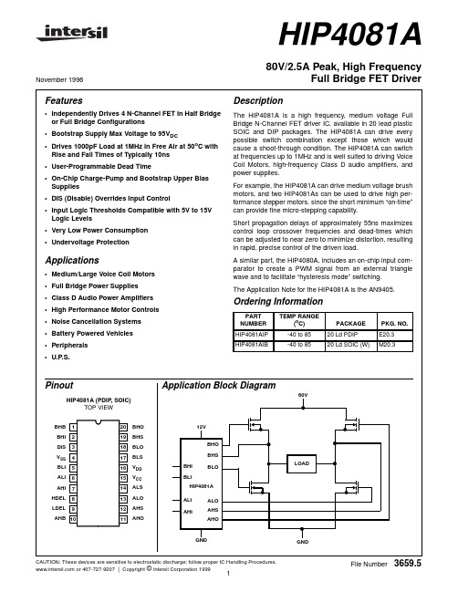
November 1996
80V/2.5A Peak, High Frequency Full Bridge FET Driver
Features
• Independently Drives 4 N-Channel FET in Half Bridge or Full Bridge Configurations
元器件交易网
HIP4081A
Absolute Maximum Ratings
Thermal Information
Supply Voltage, VDD and VCC. . . . . . . . . . . . . . . . . . . . -0.3V to 16V Logic I/O Voltages . . . . . . . . . . . . . . . . . . . . . . . -0.3V to VDD +0.3V Voltage on AHS, BHS . . . . -6.0V (Transient) to 80V (25oC to 125oC) Voltage on AHS, BHS . . . -6.0V (Transient) to 70V (-55oC to 125oC)
Supplies • DIS (Disable) Overrides Input Control • Input Logic Thresholds Compatible with 5V to 15V
Logic Levels • Very Low Power Consumption • Undervoltage Protection
Description
The HIP4081A is a high frequency, medium voltage Full Bridge N-Channel FET driver IC, available in 20 lead plastic SOIC and DIP packages. The HIP4081A can drive every possible switch combination except those which would cause a shoot-through condition. The HIP4081A can switch at frequencies up to 1MHz and is well suited to driving Voice Coil Motors, high-frequency Class D audio amplifiers, and power supplies.
74HC08中文资料_数据手册_参数
万联芯城-电子元器件采购网,提供一站式配套 ,解决物料烦恼,万联芯城-以良心做好良芯,专为终端工厂企业客 户提供电子元器件一站式配套报价服务,客户提交物料清单,商城即 可整单报价,整单下单有优惠,整单采购可节省成本,万联芯城完 善的产品供应链体系可以应对多种不同物料需求的报价, 点击进入万联芯城。
Quad 2输入和gate74HC08;74HCT08FEATURES•符合JEDEC标准no。 ESD保护:HBM EIA/ jesd22 - a114a超过2000 VMM EIA/JESD22A115-A超过200 V。•指定从- 40到+85℃和- 40到+125℃。描述:74HC/HCT08是高速硅栅CMOS器件,与低功耗肖特基晶体管(LSTTL)兼 容。它们是按照JEDECstandard no.指定的。7个。74HC/HCT08提供2-inputAND功能。快速参考数据agnd = 0 V;Tamb = 25°C;tr =tf = 6 ns.Notes1。CPD用于确定动态功耗µW (PD)。PD = CPD×VCC2×fi×N +Σ(CL×VCC2×fo)地点:fi =输入频率MHz; fo MHz =输出频 率;CL =输出负载电容在pF; VCC =供应电压伏;N =总负载切换输出;Σ(CL×VCC2×fo) = outputs.2之和。对于74HC08:条件是VI = GND 到VCC。对于74HCT08:条件是VI = GND到VCC - 1.5 V。TABLENote1函数。H =高压电平;L =低压电平Quad 2输入和 gate74HC08;74HCT08FEATURES•符合JEDEC标准no。 ESD保护:HBM EIA/ jesd22 - a114a超过2000 VMM EIA/JESD22-A115-A超过200 V。•指定从- 40到+85℃和- 40到+125℃。描述:74HC/HCT08是高速硅栅CMOS器件,与低功耗肖特基晶体管(LSTTL)兼容。它们是按照 JEDECstandard no.指定的。7个。74HC/HCT08提供2-inputAND功能。快速参考数据agnd = 0 V;Tamb = 25°C;tr =tf = 6 ns.Notes1。CPD用 于确定动态功耗µW (PD)。PD = CPD×VCC2×fi×N +Σ(CL×VCC2×fo)地点:fi =输入频率MHz; fo MHz =输出频率;CL =输出负载电容 在pF; VCC =供应电压伏;N =总负载切换输出;Σ(CL×VCC2×fo) = outputs.2之和。对于74HC08:条件是VI = GND到VCC。对于 74HCT08:条件是VI = GND到VCC - 1.5 V。TABLENote1函数。H =高压电平;L =低压电平。
凯尔贝类激光等离子电源HF440i中文手册

高压引弧的引弧板被放在等离子中.按下引弧按钮,开始引弧 。引弧结束后,高压开关自动关 闭。
位置 : 7.1 9/W a rnu ng , V o rsich t, V erb ot , G ebo t, Hinweis /War nun g ( o ran ge) / Ret tun g szeich en (gr ün)/B ren nerk op f nicht b er ühr en @ 0\m od_120 299 6 840 384 _ 19 .doc @ 36 75
警告 高压危险警告 电击会导致生命危险. 在任何维修或维护之前,请将开关关掉,并断开主电路。打开等离子机器,需要 资深电工来执行。
位置 : 7.1 2/S iche rh e it/W erk s tück ansc hli eße n und e rde n@ 0\m o d_1 200 05 2 757 236_19. doc @ 27 30
1. 操作工或维修人员在操作机器之前,必须熟悉这些标 示的意义.每个公司的公司安全手册都因该考虑这些 2.切割过程中产生的烟尘,灰尘,和气体对身体有害, 不能呼入体内.需要增加一个除尘设备 3. 穿防护衣 (头盔,焊接工人的防护罩,皮革围布,防护 手套,安全鞋). 防护衣要绝缘,干燥,防火。 4. 噪音对身体有害! 等离子切割过程中,需要带上护耳 设备. 等离子弧的辐射会导致眼痛或皮肤灼伤.保护眼睛 和皮肤是十分必要的。选择合适的防护眼镜,和保护 罩,确保有效保护。
5. 电击可导致生命危险,带电部分不可触碰. 建议电工打开等离子. 在进行任何的维护或维修之前,请断开主电路! 6. 穿防护衣 (头盔,焊接工人的防护罩,皮革围布,防护手套,安全鞋). 防护衣要绝缘,干燥,防火。操作 等离子机器,可能会导致起火或爆炸. 能导致起火或爆炸的物质须远离切割区域. 必须确保切割区域有适 当的灭火设备.这应该要写入公司安全章程。. 7. 警告标不可以撕去,喷涂,或覆盖。
HAF2008资料

HAF2008Silicon N Channel MOS FET SeriesPower SwitchingTarget specificationADE-208-707 (Z)1st. EditionDec. 1998 This FET has the over temperature shut–down capability sensing to the junction temperature. This FET has the built–in over temperature shut–down circuit in the gate area. And this circuit operation to shut–down the gate voltage in case of high junction temperature like applying over power consumption, over current etc.Features• Logic level operation (4 to 6 V Gate drive)• High endurance capability against to the short circuit• Built–in the over temperature shut–down circuit• Latch type shut–down operation (Need 0 voltage recovery)OutlineHAF20082Absolute Maximum Ratings (Ta = 25°C)ItemSymbol Ratings Unit Drain to source voltage V DSS 60V Gate to source voltage V GSS (16)V Gate to source voltage V GSS (–2.5)V Drain current I D20A Drain peak currentI D(pulse)Note140A Body-drain diode reverse drain current I DR20A Channel dissipation Pch Note230W Channel temperature Tch 150°C Storage temperature Tstg–55 to +150°CNote:1.PW ≤ 10µs, duty cycle ≤ 1 %2.Value at Ta = 25°CTypical Operation CharacteristicsItem Symbol Min Typ Max Unit Test ConditionsInput voltage V IH 3.5——V V IL —— 1.2V Input currentI IH1——100µA Vi = 8V, V DS = 0(Gate non shut down)I IH2——50µA Vi = 3.5V, V DS = 0I IL ——1µA Vi = 1.2V, V DS = 0Input currentI IH(sd)1—0.8—mA Vi = 8V, V DS = 0(Gate non shut down)I IH(sd)2—0.35—mA Vi = 3.5V, V DS = 0Shut down temperature T sd —175—°C Channel temperature Gate operation voltage V op3.5—12VHAF20083Electrical Characteristics (Ta = 25°C)Item Symbol Min Typ Max Unit Test Conditions Drain current I D1(25)——A V GS = 3.5V, V DS = 2V Drain currentI D2——10mA V GS = 1.2V, V DS = 2V Drain to source breakdown voltage V (BR)DSS 60——V I D = 10mA, V GS = 0Gate to source breakdown voltage V (BR)GSS (16)——V I G = (300µA), V DS = 0Gate to source breakdown voltage V (BR)GSS (–2.5)——V I G = (–100µA), V DS = 0Gate to source leak currentI GSS1——100µA V GS = 8V, V DS = 0I GSS2——50µA V GS = 3.5V, V DS = 0I GSS3——1µA V GS = 1.2V, V DS = 0I GSS4——–100µA V GS = –2.4V, V DS = 0Input current (shut down)I GS(op)1—0.8—mA V GS = 8V, V DS = 0I GS(op)2—0.35—mA V GS = 3.5V, V DS = 0Zero gate voltege drain current I DSS ——10µA V DS = 60 V, V GS = 0Gate to source cutoff voltage V GS(off) 1.0— 2.25V I D = 1mA, V DS = 10V Static drain to source on state resistanceR DS(on)—4560m ΩI D = 10A, V GS = 4V Note3Static drain to source on state resistanceR DS(on)—2840m ΩI D = 10A, V GS = 10V Note3Forward transfer admittance |y fs |(11)(17)—S I D = 10A, V DS = 10V Note3Output capacitance Coss —(380)—pF V DS = 10V , V GS = 0f = 1 MHz Turn-on delay time t d(on)—( )—µs I D = 10A, V GS = 5V Rise timet r —( )—µs R L = 3ΩTurn-off delay time t d(off)—( )—µs Fall timet f —( )—µs Body–drain diode forward voltage V DF —(1.0)—V I F = 20A, V GS = 0Body–drain diode reverse recovery time t rr —( )—ns I F = 20A, V GS = 0diF/ dt =50A/µs Over load shut down t os1—( )—ms V GS = 5V, V DD = 12V operation time Note4t os2—( )—msV GS = 5V, V DD = 24V Note:3.Pulse test4.Include the time shift based on increasing of chennel temperature when operete under over loadcondition.HAF2008Main Characteristics4HAF2008 Package DimensionsUnit: mm5HAF20086Cautions1.Hitachi neither warrants nor grants licenses of any rights of Hitachi’s or any third party’s patent,copyright, trademark, or other intellectual property rights for information contained in this document.Hitachi bears no responsibility for problems that may arise with third party’s rights, including intellectual property rights, in connection with use of the information contained in this document.2.Products and product specifications may be subject to change without notice. Confirm that you have received the latest product standards or specifications before final design, purchase or use.3.Hitachi makes every attempt to ensure that its products are of high quality and reliability. However,contact Hitachi’s sales office before using the product in an application that demands especially high quality and reliability or where its failure or malfunction may directly threaten human life or cause risk of bodily injury, such as aerospace, aeronautics, nuclear power, combustion control, transportation,traffic, safety equipment or medical equipment for life support.4.Design your application so that the product is used within the ranges guaranteed by Hitachi particularly for maximum rating, operating supply voltage range, heat radiation characteristics, installationconditions and other characteristics. Hitachi bears no responsibility for failure or damage when used beyond the guaranteed ranges. Even within the guaranteed ranges, consider normally foreseeable failure rates or failure modes in semiconductor devices and employ systemic measures such as fail-safes, so that the equipment incorporating Hitachi product does not cause bodily injury, fire or other consequential damage due to operation of the Hitachi product.5.This product is not designed to be radiation resistant.6.No one is permitted to reproduce or duplicate, in any form, the whole or part of this document without written approval from Hitachi.7.Contact Hitachi’s sales office for any questions regarding this document or Hitachi semiconductor products.Hitachi, Ltd.Semiconductor & IC Div.Nippon Bldg., 2-6-2, Ohte-machi, Chiyoda-ku, Tokyo 100-0004, Japan Tel: Tokyo (03) 3270-2111 Fax: (03) 3270-5109Copyright © Hitachi, Ltd., 1998. All rights reserved. Printed in Japan.Hitachi Asia Pte. Ltd.16 Collyer Quay #20-00Hitachi TowerSingapore 049318Tel: 535-2100Fax: 535-1533URLNorthAmerica : http:/Europe : /hel/ecg Asia (Singapore): .sg/grp3/sicd/index.htm Asia (Taiwan): /E/Product/SICD_Frame.htm Asia (HongKong): /eng/bo/grp3/index.htm Japan : http://www.hitachi.co.jp/Sicd/indx.htmHitachi Asia Ltd.Taipei Branch Office3F, Hung Kuo Building. No.167, Tun-Hwa North Road, Taipei (105)Tel: <886> (2) 2718-3666Fax: <886> (2) 2718-8180Hitachi Asia (Hong Kong) Ltd.Group III (Electronic Components)7/F., North Tower, World Finance Centre,Harbour City, Canton Road, Tsim Sha Tsui,Kowloon, Hong Kong Tel: <852> (2) 735 9218Fax: <852> (2) 730 0281 Telex: 40815 HITEC HXHitachi Europe Ltd.Electronic Components Group.Whitebrook ParkLower Cookham Road MaidenheadBerkshire SL6 8YA, United Kingdom Tel: <44> (1628) 585000Fax: <44> (1628) 778322Hitachi Europe GmbHElectronic components Group Dornacher Straße 3D-85622 Feldkirchen, Munich GermanyTel: <49> (89) 9 9180-0Fax: <49> (89) 9 29 30 00Hitachi Semiconductor (America) Inc.2000 Sierra Point Parkway Brisbane, CA 94005-1897Tel: <1> (800) 285-1601Fax: <1> (303) 297-0447For further information write to:。
CD4082BE中文资料

Data sheet acquired from Harris Semiconductor SCHS057C – Revised September 2003The CD4073B, CD4081B, and CD4082B types are supplied in 14-lead hermetic dual-in-line ceramic packages (F3A suffix), 14-lead dual-in-line plastic packages (E suffix), 14-lead small-outline packages (M, MT, M96, and NSR suffixes), and 14-lead thin shrink small-outline packages (PW and PWR suffixes).PACKAGING INFORMATIONOrderable Device Status(1)PackageType PackageDrawingPins PackageQtyEco Plan(2)Lead/Ball Finish MSL Peak Temp(3)7702402CA ACTIVE CDIP J141None Call TI Level-NC-NC-NC 7705102CA ACTIVE CDIP J141None Call TI Level-NC-NC-NC 7705902CA ACTIVE CDIP J141None Call TI Level-NC-NC-NC CD4073BE ACTIVE PDIP N1425Pb-Free(RoHS)CU NIPDAU Level-NC-NC-NC CD4073BF ACTIVE CDIP J141None Call TI Level-NC-NC-NC CD4073BF3A ACTIVE CDIP J141None Call TI Level-NC-NC-NCCD4073BM ACTIVE SOIC D1450Pb-Free(RoHS)CU NIPDAU Level-2-260C-1YEAR/Level-1-235C-UNLIMCD4073BM96ACTIVE SOIC D142500Pb-Free(RoHS)CU NIPDAU Level-2-260C-1YEAR/Level-1-235C-UNLIMCD4073BMT ACTIVE SOIC D14250Pb-Free(RoHS)CU NIPDAU Level-2-260C-1YEAR/Level-1-235C-UNLIMCD4073BNSR ACTIVE SO NS142000Pb-Free(RoHS)CU NIPDAU Level-2-260C-1YEAR/Level-1-235C-UNLIMCD4073BPW ACTIVE TSSOP PW1490Pb-Free(RoHS)CU NIPDAU Level-1-250C-UNLIMCD4073BPWR ACTIVE TSSOP PW142000Pb-Free(RoHS)CU NIPDAU Level-1-250C-UNLIMCD4081BE ACTIVE PDIP N1425Pb-Free(RoHS)CU NIPDAU Level-NC-NC-NC CD4081BF ACTIVE CDIP J141None Call TI Level-NC-NC-NC CD4081BF3A ACTIVE CDIP J141None Call TI Level-NC-NC-NC CD4081BFB3A ACTIVE CDIP J141None Call TI Level-NC-NC-NCCD4081BM ACTIVE SOIC D1450Pb-Free(RoHS)CU NIPDAU Level-2-260C-1YEAR/Level-1-235C-UNLIMCD4081BM96ACTIVE SOIC D142500Pb-Free(RoHS)CU NIPDAU Level-2-260C-1YEAR/Level-1-235C-UNLIMCD4081BMT ACTIVE SOIC D14250Pb-Free(RoHS)CU NIPDAU Level-2-260C-1YEAR/Level-1-235C-UNLIMCD4081BNSR ACTIVE SO NS142000Pb-Free(RoHS)CU NIPDAU Level-2-260C-1YEAR/Level-1-235C-UNLIMCD4081BPW ACTIVE TSSOP PW1490Pb-Free(RoHS)CU NIPDAU Level-1-250C-UNLIMCD4081BPWR ACTIVE TSSOP PW142000Pb-Free(RoHS)CU NIPDAU Level-1-250C-UNLIMCD4082BE ACTIVE PDIP N1425Pb-Free(RoHS)CU NIPDAU Level-NC-NC-NC CD4082BF ACTIVE CDIP J141None Call TI Level-NC-NC-NC CD4082BF3A ACTIVE CDIP J141None Call TI Level-NC-NC-NCCD4082BM ACTIVE SOIC D1450Pb-Free(RoHS)CU NIPDAU Level-2-260C-1YEAR/Level-1-235C-UNLIMCD4082BM96ACTIVE SOIC D142500Pb-Free(RoHS)CU NIPDAU Level-2-260C-1YEAR/Level-1-235C-UNLIMCD4082BMT ACTIVE SOIC D14250Pb-Free(RoHS)CU NIPDAU Level-2-260C-1YEAR/Level-1-235C-UNLIMCD4082BNSR ACTIVE SO NS142000Pb-Free(RoHS)CU NIPDAU Level-2-260C-1YEAR/Level-1-235C-UNLIMOrderable Device Status(1)PackageType PackageDrawingPins PackageQtyEco Plan(2)Lead/Ball Finish MSL Peak Temp(3)CD4082BPW ACTIVE TSSOP PW1490Pb-Free(RoHS)CU NIPDAU Level-1-250C-UNLIMCD4082BPWR ACTIVE TSSOP PW142000Pb-Free(RoHS)CU NIPDAU Level-1-250C-UNLIM JM38510/17001BCA ACTIVE CDIP J141None Call TI Level-NC-NC-NC JM38510/17002BCA ACTIVE CDIP J141None Call TI Level-NC-NC-NC JM38510/17003BCA ACTIVE CDIP J141None Call TI Level-NC-NC-NC (1)The marketing status values are defined as follows:ACTIVE:Product device recommended for new designs.LIFEBUY:TI has announced that the device will be discontinued,and a lifetime-buy period is in effect.NRND:Not recommended for new designs.Device is in production to support existing customers,but TI does not recommend using this part in a new design.PREVIEW:Device has been announced but is not in production.Samples may or may not be available.OBSOLETE:TI has discontinued the production of the device.(2)Eco Plan-May not be currently available-please check /productcontent for the latest availability information and additional product content details.None:Not yet available Lead(Pb-Free).Pb-Free(RoHS):TI's terms"Lead-Free"or"Pb-Free"mean semiconductor products that are compatible with the current RoHS requirements for all6substances,including the requirement that lead not exceed0.1%by weight in homogeneous materials.Where designed to be soldered at high temperatures,TI Pb-Free products are suitable for use in specified lead-free processes.Green(RoHS&no Sb/Br):TI defines"Green"to mean"Pb-Free"and in addition,uses package materials that do not contain halogens, including bromine(Br)or antimony(Sb)above0.1%of total product weight.(3)MSL,Peak Temp.--The Moisture Sensitivity Level rating according to the JEDECindustry standard classifications,and peak solder temperature.Important Information and Disclaimer:The information provided on this page represents TI's knowledge and belief as of the date that it is provided.TI bases its knowledge and belief on information provided by third parties,and makes no representation or warranty as to the accuracy of such information.Efforts are underway to better integrate information from third parties.TI has taken and continues to take reasonable steps to provide representative and accurate information but may not have conducted destructive testing or chemical analysis on incoming materials and chemicals.TI and TI suppliers consider certain information to be proprietary,and thus CAS numbers and other limited information may not be available for release.In no event shall TI's liability arising out of such information exceed the total purchase price of the TI part(s)at issue in this document sold by TI to Customer on an annual basis.元器件交易网IMPORTANT NOTICETexas Instruments Incorporated and its subsidiaries (TI) reserve the right to make corrections, modifications,enhancements, improvements, and other changes to its products and services at any time and to discontinueany product or service without notice. Customers should obtain the latest relevant information before placingorders and should verify that such information is current and complete. All products are sold subject to TI’s termsand conditions of sale supplied at the time of order acknowledgment.TI warrants performance of its hardware products to the specifications applicable at the time of sale inaccordance with TI’s standard warranty. T esting and other quality control techniques are used to the extent TIdeems necessary to support this warranty. Except where mandated by government requirements, testing of allparameters of each product is not necessarily performed.TI assumes no liability for applications assistance or customer product design. Customers are responsible fortheir products and applications using TI components. T o minimize the risks associated with customer productsand applications, customers should provide adequate design and operating safeguards.TI does not warrant or represent that any license, either express or implied, is granted under any TI patent right,copyright, mask work right, or other TI intellectual property right relating to any combination, machine, or processin which TI products or services are used. Information published by TI regarding third-party products or servicesdoes not constitute a license from TI to use such products or services or a warranty or endorsement thereof.Use of such information may require a license from a third party under the patents or other intellectual propertyof the third party, or a license from TI under the patents or other intellectual property of TI.Reproduction of information in TI data books or data sheets is permissible only if reproduction is withoutalteration and is accompanied by all associated warranties, conditions, limitations, and notices. Reproductionof this information with alteration is an unfair and deceptive business practice. TI is not responsible or liable forsuch altered documentation.Resale of TI products or services with statements different from or beyond the parameters stated by TI for thatproduct or service voids all express and any implied warranties for the associated TI product or service andis an unfair and deceptive business practice. TI is not responsible or liable for any such statements.Following are URLs where you can obtain information on other Texas Instruments products and applicationsolutions:Products ApplicationsAmplifiers Audio /audioData Converters Automotive /automotiveDSP Broadband /broadbandInterface Digital Control /digitalcontrolLogic Military /militaryPower Mgmt Optical Networking /opticalnetworkMicrocontrollers Security /securityTelephony /telephonyVideo & Imaging /videoWireless /wirelessMailing Address:Texas InstrumentsPost Office Box 655303 Dallas, Texas 75265Copyright 2005, Texas Instruments Incorporated。
- 1、下载文档前请自行甄别文档内容的完整性,平台不提供额外的编辑、内容补充、找答案等附加服务。
- 2、"仅部分预览"的文档,不可在线预览部分如存在完整性等问题,可反馈申请退款(可完整预览的文档不适用该条件!)。
- 3、如文档侵犯您的权益,请联系客服反馈,我们会尽快为您处理(人工客服工作时间:9:00-18:30)。
HCC/HCF40208BJune 19894x 4MULTIPORT REGISTERDESCRIPTION.FOUR 4-BIT REGISTERS.ONE INPUT AND TWO OUTPUT BUSES.UNLIMITED EXPANSION IN BIT AND WORD DIRECTIONS.DATA LINES HAVE LATCHED INPUTS .3-STATE OUTPUTS.SEPARATE CONTROL OF EACH BUS,ALLOWING SIMULTANEOUS INDEPENDENT READING OF ANY OF FOUR REGISTERS ON BUS A AND BUS B AND INDEPENDENT WRIT-ING INTO ANY OF THE FOUR REGISTERS .40108B IS PIN-COMPATIBLE WITH INDUS-TRY TYPE MC14580.STANDARDIZED,SYMMETRICAL OUTPUT CHARACTERISTICS.QUIESCENT CURRENT SPECIFIED AT 20V FOR HCC DEVICE.5V,10V,AND 15V PARAMETRIC RATINGS .INPUT CURRENT OF 100nA AT 18V AND 25°C FOR HCC DEVICE.100%TESTED FOR QUIESCENT CURRENT .MEETS ALL REQUIREMENTS OF JEDECTEN-TATIVE STANDARDN °13A,”STANDARD SPE-CIFICATIONS FOR DESCRIPTION OF ”B”SERIES CMOS DEVICES”BEY(Plastic Package)BF(Ceramic Frit Seal Package)BM1(Micro Package )ORDER CODES :HCC40208BF HCF40208BEYHCF40208BM1PIN CONNECTIONSThe HCC40208B (extended temperature range)and HCF40208B (intermediate temperature range)are monolithic integrated circuits,available in 24-lead dual in-line plastic or ceramic package and plastic micro package.The HCC/HCF40208B is a 4x 4multiport register containing four 4-bit registers,write address decoder,two separate read address decoders,and two 3-state output buses.When the ENABLE input is low,the corresponding output bus is switched,inde-pendently of the clock to a high-impedance state.The high-impedance third state provides the outputs with the capability of being connected to the bus lines in a bus-organized system without the need for interface or pull-up components.When the WRITE ENABLE input is high,all data input lines are latched on the positive transition of the CLOCKand the data is entered into the wordselected bythewrite address lines.When WRITE ENABLE is low,the CLOCK is inhibited and no new data isentered.In either case,the contents ofany word may be accessed via the read address lines inde-pendent of the state of the CLOCK input.1/13ABSOLUTE MAXIMUM RATINGSSymbol Parameter Value UnitV DD*Supply Voltage:HCC TypesHCF Types –0.5to+20–0.5to+18VVV i Input Voltage–0.5to V DD+0.5V I I DC Input Current(any one input)±10mAP t o t Total Power Dissipation(per package)Dissipation per Output Transistorfor T o p=Full Package-temperature Range 200100mWmWT o p Operating Temperature:HCC TypesHCF Types –55to+125–40to+85°C°CT s t g Storage Temperature–65to+150°C Stresses above those listed under”Absolute Maximum Ratings”may cause permanent damage to the device.This is a stress rating only and functional operation of the device at these or any other conditions above those indicated in the operational sections of this specification is not implied.Exposure to absolute maximum rating conditions for external periods may affect device reliability. *All voltages are with respect to V SS(GND).FUNCTIONAL DIAGRAMRECOMMENDED OPERATING CONDITIONSSymbol Parameter Value UnitV DD Supply Voltage:HCC TypesHCF Types 3to183to15VVV I Input Voltage0to V DD VT o p Operating Temperature:HCC TypesHCF Types –55to+125–40to+85°C°CHCC/HCF40208B 2/13HCC/HCF40208B SCHEMATIC DIAGRAM3/13HCC/HCF40208B LOGIC DIAGRAMTIMING DIAGRAM 4/13STATIC ELECTRICAL CHARACTERISTICS (over recommended operating conditions)Test ConditionsValueV IV O |I O |V D D T L o w *25°CT Hi g h *SymbolParameter (V)(V)(µA)(V)Min.Max.Min.Typ.Max.Min.Max.UnitI LQuiescent CurrentHCC Types 0/5550.045150µA0/1010100.04103000/1515200.04206000/20201000.081003000HCF Types0/55200.04201500/1010400.04403000/1515800.0480600V OHOutput High Voltage 0/5<15 4.95 4.95 4.95V0/10<1109.959.959.950/15<11514.9514.9514.95V OLOutput Low Voltage 5/0<150.050.050.05V10/0<1100.050.050.0515/0<1150.050.050.05V IHInput High Voltage 0.5/4.5<15 3.5 3.5 3.5V1/9<1107771.5/13.5<115111111V ILInput Low Voltage 4.5/0.5<15 1.5 1.5 1.5V9/1<11033313.5/1.5<115444I OHOutput Drive CurrentHCC Types0/5 2.55–2–1.6–3.2–1.15mA0/5 4.65–0.64–0.51–1–0.360/109.510–1.6–1.3–2.6–0.90/1513.515–4.2–3.4–6.8–2.4HCF Types0/5 2.55–1.53–1.36–3.2–1.10/5 4.65–0.52–0.44–1–0.360/109.510–1.3–1.1–2.6–0.90/1513.515–3.6–3.0–6.8–2.4*T Low =–55°C for HCC device :–40°C for HCF device.*T High =+125°C for HCC device :+85°C for HCF device.The Noise Margin for both ”1”and ”0”level is :1V min.with V DD =5V,2V min.with V DD =10V,2.5V min.with V DD =15V.**Forced output disable.TRUTH TABLEClock Write Enable Write 1Write 0Read 1A Read 0A Read 1B Read 0BEnableA EnableB D n Q n A Q n B –/–1S1S2S1S2S1S211111–/–1S1S2S1S2S1S211000X X X X X X X X 00X Z Z –/–11111D n to Word 0Word 1Out Word 2Out –/–000011011Word 0Not Altered Word 1Out Word 2Out X X X X 100111X Word 2Out Word 1Out –\–XXXXXXX11XNCNC1=HIGH LEVEL,0=LOW LEVEL,X =DON’T CARE,Z =HIGH IMPEDANCE.S1and S2refer to input strates of either 1or 0.HCC/HCF40208B5/13STATIC ELECTRICAL CHARACTERISTICS(continued)Test Conditions ValueV I V O|I O|V D D T L o w*25°C T Hi g h*Symbol Parameter(V)(V)(µA)(V)Min.Max.Min.Typ.Max.Min.Max.UnitI OL OutputSinkCurrent HCCTypes0/50.450.640.5110.36mA 0/100.510 1.6 1.3 2.60.90/15 1.515 4.2 3.4 6.8 2.4HCFTypes0/50.450.520.4410.360/100.510 1.3 1.1 2.60.90/15 1.515 3.6 3.0 6.8 2.4I IH,I IL InputLeakageCurrent HCCTypes0/18Any Input18±0.1±10–5±0.1±1µA HCFTypes0/1515±0.3±10–5±0.3±1I O H,I O L**3-StateOutputLeakageCurrent HCCTypes0/180/1818±0.4±10–4±0.4±12µA HCFTypes0/150/1515±1.0±10–4±1.0±7.5C I Input Capacitance Any Input57.5pF *T Low=–55°C for HCC device:–40°C for HCF device.*T High=+125°C for HCC device:+85°C for HCF device.The Noise Margin for both”1”and”0”level is:1V min.with V DD=5V,2V min.with V DD=10V,2.5V min.with V DD=15V. **Forced output disable.DYNAMIC ELECTRICAL CHARACTERISTICS(T amb=25°C,C L=50pF,R L=200kΩ,typical temperature coefficient for all V DD values is0.3%/°C,all input rise and fall time=20ns)Test Conditions ValueSymbol ParameterV D D(V)Min.Typ.Max.Unitt PHL, t P L H Propagation Delay Time:Clock to Write Enable to Q5360720ns1014028015100200Read or Write Address to Q5300600ns101202401585170t PZH, t P HZ 3-state Disable Delay Time5100200ns1050100154080t PZ L, t PL Z 3-State Disable Delay time5130260ns10601201550100t T HL, t T L H Output Transition Time5100200ns1050100154080t s e t u p Setup TimeData to Clock t s(D)50–95ns 100–35150–20Write Enable to Clock t s(WE)5250125ns1010050157035Write Address to Clock t s(WA)5250125ns1010050157035HCC/HCF40208B6/13DYNAMIC ELECTRICAL CHARACTERISTICS(continued)Test Conditions ValueSymbol ParameterV D D(V)Min.Typ.Max.Unit t r,t f Clock Rise and Fall Time515µs105155t h o l d Hold TimeData to Clock t h(D)5220110ns 1010050158040Write Enable to Clock t h(WE)5270135ns1013065158040Write Address to Clock t s(WA)53301651014070159045t W Clock Pulse WidthClock or Write Enable t W(CL)5350175ns 1013065159045Write Address t W(WA)5300150ns1015075159045f CL Maximum Clock Input Frequency5 1.53MHz10 3.5715 4.59Output Low(sink)Current Characteristics.Output High(source)Current Characteristics.HCC/HCF40208B7/13Typical Propagation Delay Time vs.Load Capacit-ance (CL or WE to Q).Typical Transition Time vs.Load Capacitance.TEST CIRCUITSOutput-enable-delay-times and Waveforms.Typical Dynamic Power Dissipation vs.Input Fre-quency.HCC/HCF40208B8/13HCC/HCF40208B Power-d issipation and Waveforms.Quiescent Device Current.Input Voltage.Input Current.9/13HCC/HCF40208BPlastic DIP24(0.25)MECHANICAL DATAmm inch DIM.MIN.TYP.MAX.MIN.TYP.MAX.a10.630.025b0.450.018b10.230.310.0090.012 b2 1.270.050D32.2 1.268 E15.216.680.5980.657e 2.540.100e327.94 1.100F14.10.555I 4.4450.175L 3.30.130P043A 10/13HCC/HCF40208B Ceramic DIP24MECHANICAL DATAmm inchDIM.MIN.TYP.MAX.MIN.TYP.MAX.A32.3 1.272B13.0513.360.5140.526C 3.9 5.080.1540.200D30.118E0.5 1.780.0200.070e327.94 1.100F 2.29 2.790.0900.110G0.40.550.0160.022I 1.17 1.520.0460.060L0.220.310.0090.012M 1.52 2.490.0600.098N14°(min.),15°(max.)P15.415.80.6060.622Q 5.710.225P058C11/13SO24MECHANICAL DATADIM.mm inch MIN.TYP.MAX.MIN.TYP.MAX.A 2.650.104a10.100.200.0040.007a2 2.450.096b 0.350.490.0130.019b10.230.320.0090.012C 0.500.020c145°(typ.)D 15.2015.600.5980.614E 10.0010.650.3930.420e 1.270.05e313.970.55F 7.407.600.2910.299L 0.50 1.270.190.050S8°(max.)FCLEa 1b 1Ae De3b 2413112c1sa 2HCC/HCF40208B12/13HCC/HCF40208B Information furnished is believed to be accurate and reliable.However,SGS-THOMSON Microelectronics assumes no responsability for the consequences of use of such information nor for any infringement of patents or other rights of third parties which may results from its use.No license is granted by implication or otherwise under any patent or patent rights of SGS-THOMSON Microelectronics.Specificationsmentioned in this publication are subject to change without notice.This publication supersedes and replaces all information previously supplied.SGS-THOMSON Microelectronics products are not authorized for use ascritical components in life support devices or systems without express written approval of SGS-THOMSON Microelectonics.©1994SGS-THOMSON Microelectronics-All Rights ReservedSGS-THOMSON Microelectronics GROUP OF COMPANIESAustralia-Brazil-France-Germany-Hong Kong-Italy-Japan-Korea-Malaysia-Malta-Morocco-The Netherlands-Singapore-Spain-Sweden-Switzerland-Taiwan-Thailand-United Kingdom-U.S.A13/13。