HD74HC375P中文资料
HD74HC09P中文资料

HD74HC09Quad. 2-input AND Gates (with open drain outputs)ADE-205-409 (Z)1st. EditionSep. 2000 Features• High Speed Operation: t pd = 8 ns typ (C L = 50 pF)• High Output Current: Fanout of 10 LSTTL Loads• Wide Operating Voltage: V CC = 2 to 6 V• Low Input Current: 1 µA max• Low Quiescent Supply Current: I CC (static) = 1 µA max (Ta = 25°C)Pin ArrangementHD74HC092DC CharacteristicsTa = 25°CTa = –40 to +85°CItem Symbol V CC (V)Min Typ Max MinMax Unit Test ConditionsInput voltageV IH2.0 1.5—— 1.5—V4.5 3.15—— 3.15—6.04.2—— 4.2—V IL2.0——0.5—0.5V 4.5—— 1.35—1.356.0——1.8— 1.8Output voltageV OL2.0—0.00.1—0.1VVin = V IH or V IL I OL = 20 µA4.5—0.00.1—0.16.0—0.00.1—0.14.5——0.26—0.33I OL = 4 mA 6.0——0.26—0.33I OL = 5.2 mAOff-state output current Io (off) 6.0——±0.5—±5.0µA Vin = V IH or V ILVout = V CC or GND Input current Iin 6.0——±0.1—±1.0µA Vin = V CC or GNDQuiescent supply currentI CC6.0——1.0—10µAVin = V CC or GND, Iout = 0 µAAC Characteristics (C L = 50 pF, Input t r = t f = 6 ns)Ta = 25°CTa = –40 to +85°CItem SymbolV CC (V)Min Typ Max MinMax Unit Test ConditionsPropagation delay t PLH2.0——90—115nstime4.5—1018—236.0——15—20t PHL 2.0——90—115ns 4.5—618—236.0——15—20Output fall timet THL2.0——75—95ns 4.5—515—196.0——13—16Input capacitanceCin——510—10pFHD74HC09 Package Dimensions3HD74HC094HD74HC095Cautions1.Hitachi neither warrants nor grants licenses of any rights of Hitachi’s or any third party’s patent,copyright, trademark, or other intellectual property rights for information contained in this document.Hitachi bears no responsibility for problems that may arise with third party’s rights, includingintellectual property rights, in connection with use of the information contained in this document.2.Products and product specifications may be subject to change without notice. Confirm that you have received the latest product standards or specifications before final design, purchase or use.3.Hitachi makes every attempt to ensure that its products are of high quality and reliability. However,contact Hitachi’s sales office before using the product in an application that demands especially high quality and reliability or where its failure or malfunction may directly threaten human life or cause risk of bodily injury, such as aerospace, aeronautics, nuclear power, combustion control, transportation,traffic, safety equipment or medical equipment for life support.4.Design your application so that the product is used within the ranges guaranteed by Hitachi particularly for maximum rating, operating supply voltage range, heat radiation characteristics, installationconditions and other characteristics. Hitachi bears no responsibility for failure or damage when used beyond the guaranteed ranges. Even within the guaranteed ranges, consider normally foreseeable failure rates or failure modes in semiconductor devices and employ systemic measures such as fail-safes, so that the equipment incorporating Hitachi product does not cause bodily injury, fire or other consequential damage due to operation of the Hitachi product.5.This product is not designed to be radiation resistant.6.No one is permitted to reproduce or duplicate, in any form, the whole or part of this document without written approval from Hitachi.7.Contact Hitachi’s sales office for any questions regarding this document or Hitachi semiconductor products.Hitachi, Ltd.Semiconductor & Integrated Circuits.Nippon Bldg., 2-6-2, Ohte-machi, Chiyoda-ku, Tokyo 100-0004, Japan Tel: Tokyo (03) 3270-2111 Fax: (03) 3270-5109Copyright © Hitachi, Ltd., 2000. All rights reserved. Printed in Japan.Hitachi Asia Ltd. Hitachi Tower16 Collyer Quay #20-00, Singapore 049318Tel : <65>-538-6533/538-8577 Fax : <65>-538-6933/538-3877URL : .sg URLNorthAmerica : /Europe : /hel/ecg Asia : Japan : http://www.hitachi.co.jp/Sicd/indx.htmHitachi Asia Ltd.(Taipei Branch Office)4/F, No. 167, Tun Hwa North Road, Hung-Kuo Building, Taipei (105), Taiwan Tel : <886>-(2)-2718-3666 Fax : <886>-(2)-2718-8180 Telex : 23222 HAS-TPURL : Hitachi Asia (Hong Kong) Ltd. Group III (Electronic Components) 7/F., North Tower, World Finance Centre,Harbour City, Canton Road Tsim Sha Tsui, Kowloon, Hong KongTel : <852>-(2)-735-9218 Fax : <852>-(2)-730-0281URL : Hitachi Europe Ltd.Electronic Components Group.Whitebrook ParkLower Cookham Road MaidenheadBerkshire SL6 8YA, United Kingdom Tel: <44> (1628) 585000Fax: <44> (1628) 585160Hitachi Europe GmbHElectronic Components Group Dornacher Stra βe 3D-85622 Feldkirchen, Munich GermanyTel: <49> (89) 9 9180-0Fax: <49> (89) 9 29 30 00Hitachi Semiconductor (America) Inc.179 East Tasman Drive,San Jose,CA 95134 Tel: <1> (408) 433-1990Fax: <1>(408) 433-0223For further information write to:Colophon 2.0。
HD74HC240P中文资料

HD74HC240Octal Buffers/Line Drivers/Line Receivers(with inverted 3-state outputs)REJ03D0594–0200(Previous ADE-205-471)Rev.2.00Jan 31, 2006 DescriptionThe HD74HC240 is an inverting buffer and has two active low enables (1G and 2G). Each enable independently controls 4 buffers. This device does not have schmitt trigger inputs.Features• High Speed Operation: t pd = 10 ns typ (C L = 50 pF)• High Output Current: Fanout of 15 LSTTL Loads• Wide Operating Voltage: V CC = 2 to 6 V• Low Input Current: 1 µA max• Low Quiescent Supply Current: I CC (static) = 4 µA max (Ta = 25°C)• Ordering InformationPart Name Package TypePackage Code(Previous Code)PackageAbbreviationTaping Abbreviation(Quantity)HD74HC240P DILP-20pin PRDP0020AC-B(DP-20NEV)P —HD74HC240FPEL SOP-20 pin (JEITA) PRSP0020DD-B(FP-20DAV)FP EL (2,000 pcs/reel)HD74HC240RPEL SOP-20 pin (JEDEC) PRSP0020DC-A(FP-20DBV)RP EL (1,000 pcs/reel)HD74HC240TELL TSSOP-20pin PTSP0020JB-A(TTP-20DAV)T ELL (2,000 pcs/reel)Note: Please consult the sales office for the above package availability.Function TableInputs OutputG A YH X ZL H LL L HH : high levelL : low levelX : irrelevantZ : off (high-impedance) state of a 3-state outputPin ArrangementLogic DiagramAbsolute Maximum RatingsItem Symbol Ratings UnitSupply voltage range V CC –0.5 to 7.0 V Input / Output voltage V IN , V OUT –0.5 to V CC +0.5 V Input / Output diode current I IK , I OK ±20 mA Output current I O ±35 mA V CC , GND current I CC or I GND ±75 mA Power dissipation P T 500 mW Storage temperature Tstg –65 to +150 °C Note: The absolute maximum ratings are values, which must not individually be exceeded, and furthermore, no two ofwhich may be realized at the same time.Recommended Operating ConditionsItem Symbol Ratings Unit ConditionsSupply voltage V CC 2 to 6 V Input / Output voltage V IN , V OUT 0 to V CC V Operating temperature Ta –40 to 85 °C 0 to 1000 V CC = 2.0 V0 to 500 V CC = 4.5 V Input rise / fall time *1 t r , t f 0 to 400 ns V CC = 6.0 V Notes: 1. This item guarantees maximum limit when one input switches.Waveform: Refer to test circuit of switching characteristics.Electrical CharacteristicsTa = 25°C Ta = –40 to+85°CItem Symbol V CC (V)Min Typ Max Min MaxUnitTest Conditions2.0 1.5 — — 1.5— 4.5 3.15 — — 3.15 — V IH6.0 4.2 — — 4.2 —V 2.0 — — 0.5 — 0.5 4.5 — — 1.35 — 1.35Input voltageV IL6.0 — — 1.8 — 1.8V 2.0 1.9 2.0 — 1.9 — 4.5 4.4 4.5 — 4.4 — 6.0 5.9 6.0 — 5.9 — I OH = –20 µA 4.5 4.18 — — 4.13 — I OH = –6 mA V OH6.0 5.68 — — 5.63— V Vin = V IH or V IL I OH = –7.8 mA2.0 — 0.0 0.1 —0.1 4.5 — 0.0 0.1 — 0.1 6.0 — 0.0 0.1 — 0.1 I OL = 20 µA 4.5 — — 0.26 — 0.33 I OL = 6 mA Output voltage V OL6.0 — — 0.26 —0.33 V Vin = V IH or V IL I OL = 7.8 mA Off-state output currentI OZ 6.0— — ±0.5 — ±5.0 µA Vin = V IH or V IL ,Vout = V CC or GNDInput current Iin 6.0 — — ±0.1 — ±1.0 µA Vin = V CC or GNDQuiescent supply current I CC 6.0— — 4.0 — 40 µA Vin = V CC or GND, Iout = 0 µASwitching Characteristics(C L = 50 pF, Input t r = t f = 6 ns)Ta = 25°C Ta = –40 to +85°CItem Symbol V CC (V)Min Typ Max Min MaxUnitTest Conditions2.0 — — 90 — 115 4.5 — 10 18 — 23 t PHL6.0 — — 15 — 20 ns 2.0 — — 90 — 115 4.5 — 10 18 — 23 Propagation delaytimet PLH6.0 — — 15 — 20 ns 2.0 — — 150 — 190 4.5 — 11 30 — 38 t ZL6.0 — — 26 — 33 ns 2.0 — — 150 — 190 4.5 — 12 30 — 38 Output enable time t ZH6.0 — — 26 — 33 ns 2.0 — — 150 — 190 4.5 — 16 30 — 38 t LZ6.0 — — 26 — 33 ns 2.0 — — 150 — 190 4.5 — 19 30 — 38 Output disabletimet HZ6.0 — — 26 —33 ns 2.0 — — 60 —75 4.5 — 4 12 — 15 Output rise/fall timet TLH t THL 6.0 — — 10 — 13 ns Input capacitance Cin— — 5 10—10 pFTest CircuitWaveformsPackage Dimensions RENESAS SALES OFFICESRefer to "/en/network" for the latest and detailed information.Renesas Technology America, Inc.450 Holger Way, San Jose, CA 95134-1368, U.S.ATel: <1> (408) 382-7500, Fax: <1> (408) 382-7501Renesas Technology Europe LimitedDukes Meadow, Millboard Road, Bourne End, Buckinghamshire, SL8 5FH, U.K.Tel: <44> (1628) 585-100, Fax: <44> (1628) 585-900Renesas Technology (Shanghai) Co., Ltd.Unit 205, AZIA Center, No.133 Yincheng Rd (n), Pudong District, Shanghai 200120, ChinaTel: <86> (21) 5877-1818, Fax: <86> (21) 6887-7898Renesas Technology Hong Kong Ltd.7th Floor, North Tower, World Finance Centre, Harbour City, 1 Canton Road, Tsimshatsui, Kowloon, Hong KongTel: <852> 2265-6688, Fax: <852> 2730-6071Renesas Technology Taiwan Co., Ltd.10th Floor, No.99, Fushing North Road, Taipei, TaiwanTel: <886> (2) 2715-2888, Fax: <886> (2) 2713-2999Renesas Technology Singapore Pte. Ltd.1 Harbour Front Avenue, #06-10, Keppel Bay Tower, Singapore 098632Tel: <65> 6213-0200, Fax: <65> 6278-8001Renesas Technology Korea Co., Ltd.Kukje Center Bldg. 18th Fl., 191, 2-ka, Hangang-ro, Yongsan-ku, Seoul 140-702, KoreaTel: <82> (2) 796-3115, Fax: <82> (2) 796-2145Renesas Technology Malaysia Sdn. BhdUnit 906, Block B, Menara Amcorp, Amcorp Trade Centre, No.18, Jalan Persiaran Barat, 46050 Petaling Jaya, Selangor Darul Ehsan, MalaysiaTel: <603> 7955-9390, Fax: <603> 7955-9510© 2006. Renesas Technology Corp., All rights reserved. Printed in Japan.。
HD74HC368P中文资料

4.5
— — 0.26 — 0.33
6.0
— — 0.26 — 0.33
I OZ
6.0
— — ±0.5 — ±5.0 µA
Iin
6.0
— — ±0.1 — ±1.0 µA
HD74HC75RPEL中文资料
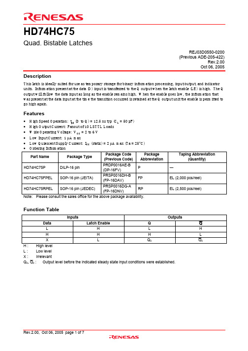
HD74HC75Quad. Bistable LatchesREJ03D0550-0200(Previous ADE-205-422)Rev.2.00Oct 06, 2005 DescriptionThis latch is ideally suited for use as temporary storage for binary information processing, input/output, and indicator units. Information present at the data (D) input is transferred to the Q output when the latch enable (LE) is high. The Q output will follow the data input as long as the enable remains high. When the enable goes low, the information that was present at the data input at the time the transition occurred is retained at the Q output unit the enable is permitted to go high again.Features• High Speed Operation: t pd (D to Q) = 12.5 ns typ (C L = 50 pF)• High Output Current: Fanout of 10 LSTTL Loads• Wide Operating Voltage: V CC = 2 to 6 V• Low Input Current: 1 µA max• Low Quiescent Supply Current: I CC (static) = 2 µA max (Ta = 25°C)• Ordering InformationPart Name Package TypePackage Code(Previous Code)PackageAbbreviationTaping Abbreviation(Quantity)HD74HC75P DILP-16pin PRDP0016AE-B(DP-16FV)P —HD74HC75FPEL SOP-16 pin (JEITA) PRSP0016DH-B(FP-16DAV)FP EL (2,000 pcs/reel)HD74HC75RPEL SOP-16 pin (JEDEC) PRSP0016DG-A(FP-16DNV)RP EL (2,500 pcs/reel)Note: Please consult the sales office for the above package availability.Function TableInputs Outputs Data LatchEnable Q QL H L HH H H LX L Q0Q0H : High levelL : Low levelX : IrrelevantQ0, Q0 : Output level before the indicated steady state input conditions were established.Pin ArrangementLogic Diagram (1/4)Absolute Maximum RatingsUnit Item SymbolRatingsSupply voltage range V CC–0.5 to 7.0 VInput / Output voltage Vin, Vout –0.5 to V CC +0.5 VInput / Output diode current I IK, I OK±20 mA Output current I O±25 mAV CC, GND current I CC or I GND±50 mAmW Power dissipation P T 500Storage temperature Tstg –65 to +150 °CNote: The absolute maximum ratings are values, which must not individually be exceeded, and furthermore, no two of which may be realized at the same time.Recommended Operating ConditionsItem Symbol Ratings Unit ConditionsSupply voltageV CC 2 to 6 VInput / Output voltage V IN , V OUT 0 to V CC V Operating temperature Ta –40 to 85 °C0 to 1000 V CC = 2.0 V0 to 500 V CC = 4.5 VInput rise / fall time *1t r , t f0 to 400ns V CC = 6.0 VNote: 1. This item guarantees maximum limit when one input switches.Waveform: Refer to test circuit of switching characteristics.Electrical CharacteristicsTa = 25°CTa = –40 to+85°CItem Symbol V CC (V) Min Typ Max Min Max UnitTest Conditions2.0 1.5 — — 1.5 — 4.53.15 — — 3.15 —V IH 6.0 4.2 — — 4.2 —V2.0 — — 0.5 — 0.5 4.5 — — 1.35 — 1.35Input voltage V IL6.0 — — 1.8 — 1.8 V 2.0 1.9 2.0 — 1.9 — 4.5 4.4 4.5 — 4.4 — 6.0 5.9 6.0 — 5.9 — I OH = –20 µA 4.5 4.18 — — 4.13 — I OH = –4 mA V OH6.0 5.68 — — 5.63 —V Vin = V IH or V IL I OH = –5.2 mA2.0 — 0.0 0.1 — 0.1 4.5 — 0.0 0.1 — 0.1 6.0 — 0.0 0.1 — 0.1 I OL = 20 µA 4.5 — — 0.26 — 0.33I OL = 4 mAOutput voltage V OL6.0 — — 0.26 — 0.33 V Vin = V IH or V IL I OL = 5.2 mA Input current Iin6.0 — — ±0.1 — ±1.0 µA Vin = V CC or GNDQuiescent supplycurrent I CC 6.0 — — 2.0 — 20 µA Vin = V CC or GND, Iout = 0 µASwitching Characteristics (C L = 50 pF, Input t r = t f = 6 ns)Ta = 25°C Ta = –40 to +85°CItem Symbol V CC (V) Min Typ Max Min Max UnitTest Conditions2.0 — — 125 — 155 4.5 — 12 25 — 31 6.0 — — 21 — 26 ns Data to Q 2.0 — — 110 — 140 4.5 — 13 22 — 28 6.0 — — 19 — 24ns Data to Q 2.0 — — 145 — 180 4.5 — 12 29 — 36 6.0 — — 25 — 31ns Latch Enable to Q 2.0 — — 125 — 155 4.5 — 13 25 — 31Propagation delay timet PLH , t PHL6.0 — — 21 — 26ns Latch Enable to QSwitching Characteristics (C L = 50 pF, Input t r = t f = 6 ns)Ta = 25°CTa = –40 to +85°CItem Symbol V CC (V) Min Typ Max Min Max Unit Test Conditions2.0 100 — — 125 — 4.5 20 4 — 25 —Setup time t su 6.0 17 — — 21 —nsData to Latch Enable2.0 5 — — 5 — 4.5 5 0 — 5 —Hold timet h6.0 5 — — 5 —ns Latch Enable to Data 2.0 80 — — 100 — 4.5 16 5 — 20 — Pulse width t w6.0 14 — — 17 —ns Latch Enable 2.0 — — 75 — 95 4.5 — 5 15 — 19 Output rise/fall timet TLH , t THL6.0 — — 13 — 16 ns Input capacitance Cin— — 5 10 — 10 pFTest CircuitWaveformsPackage Dimensions RENESAS SALES OFFICESRefer to "/en/network" for the latest and detailed information.Renesas Technology America, Inc.450 Holger Way, San Jose, CA 95134-1368, U.S.ATel: <1> (408) 382-7500, Fax: <1> (408) 382-7501Renesas Technology Europe LimitedDukes Meadow, Millboard Road, Bourne End, Buckinghamshire, SL8 5FH, U.K.Tel: <44> (1628) 585-100, Fax: <44> (1628) 585-900Renesas Technology Hong Kong Ltd.7th Floor, North Tower, World Finance Centre, Harbour City, 1 Canton Road, Tsimshatsui, Kowloon, Hong KongTel: <852> 2265-6688, Fax: <852> 2730-6071Renesas Technology Taiwan Co., Ltd.10th Floor, No.99, Fushing North Road, Taipei, TaiwanTel: <886> (2) 2715-2888, Fax: <886> (2) 2713-2999Renesas Technology (Shanghai) Co., Ltd.Unit2607 Ruijing Building, No.205 Maoming Road (S), Shanghai 200020, ChinaTel: <86> (21) 6472-1001, Fax: <86> (21) 6415-2952Renesas Technology Singapore Pte. Ltd.1 Harbour Front Avenue, #06-10, Keppel Bay Tower, Singapore 098632Tel: <65> 6213-0200, Fax: <65> 6278-8001Renesas Technology Korea Co., Ltd.Kukje Center Bldg. 18th Fl., 191, 2-ka, Hangang-ro, Yongsan-ku, Seoul 140-702, KoreaTel: <82> 2-796-3115, Fax: <82> 2-796-2145Renesas Technology Malaysia Sdn. Bhd.Unit 906, Block B, Menara Amcorp, Amcorp Trade Centre, No.18, Jalan Persiaran Barat, 46050 Petaling Jaya, Selangor Darul Ehsan, MalaysiaTel: <603> 7955-9390, Fax: <603> 7955-9510。
HD74LS375FPEL中文资料
Hitachi CodeJEDECEIAJWeight (reference value)DP-16 Conforms Conforms 1.07 gHitachi Code JEDEC EIAJWeight (reference value)FP-16DA —Conforms 0.24 g*Dimension including the plating thicknessBase material dimension° – 8°Hitachi CodeJEDECEIAJWeight (reference value)FP-16DNConformsConforms0.15 gUnit: mm*Dimension including the plating thickness Base material dimension° – 8°元器件交易网Cautions1.Hitachi neither warrants nor grants licenses of any rights of Hitachi’s or any third party’s patent,copyright, trademark, or other intellectual property rights for information contained in this document.Hitachi bears no responsibility for problems that may arise with third party’s rights, includingintellectual property rights, in connection with use of the information contained in this document.2.Products and product specifications may be subject to change without notice. Confirm that you have received the latest product standards or specifications before final design, purchase or use.3.Hitachi makes every attempt to ensure that its products are of high quality and reliability. However,contact Hitachi’s sales office before using the product in an application that demands especially high quality and reliability or where its failure or malfunction may directly threaten human life or cause risk of bodily injury, such as aerospace, aeronautics, nuclear power, combustion control, transportation,traffic, safety equipment or medical equipment for life support.4.Design your application so that the product is used within the ranges guaranteed by Hitachi particularly for maximum rating, operating supply voltage range, heat radiation characteristics, installationconditions and other characteristics. Hitachi bears no responsibility for failure or damage when used beyond the guaranteed ranges. Even within the guaranteed ranges, consider normally foreseeable failure rates or failure modes in semiconductor devices and employ systemic measures such as fail-safes, so that the equipment incorporating Hitachi product does not cause bodily injury, fire or other consequential damage due to operation of the Hitachi product.5.This product is not designed to be radiation resistant.6.No one is permitted to reproduce or duplicate, in any form, the whole or part of this document without written approval from Hitachi.7.Contact Hitachi’s sales office for any questions regarding this document or Hitachi semiconductor products.Hitachi, Ltd.Semiconductor & Integrated Circuits.Nippon Bldg., 2-6-2, Ohte-machi, Chiyoda-ku, Tokyo 100-0004, Japan Tel: Tokyo (03) 3270-2111 Fax: (03) 3270-5109Copyright ' Hitachi, Ltd., 1999. All rights reserved. Printed in Japan.Hitachi Asia Pte. Ltd.16 Collyer Quay #20-00Hitachi TowerSingapore 049318Tel: 535-2100Fax: 535-1533URLNorthAmerica : http:/Europe : /hel/ecg Asia (Singapore): .sg/grp3/sicd/index.htm Asia (Taiwan): /E/Product/SICD_Frame.htm Asia (HongKong): /eng/bo/grp3/index.htm Japan : http://www.hitachi.co.jp/Sicd/indx.htmHitachi Asia Ltd.Taipei Branch Office3F, Hung Kuo Building. No.167, Tun-Hwa North Road, Taipei (105)Tel: <886> (2) 2718-3666Fax: <886> (2) 2718-8180Hitachi Asia (Hong Kong) Ltd.Group III (Electronic Components)7/F., North Tower, World Finance Centre,Harbour City, Canton Road, Tsim Sha Tsui,Kowloon, Hong Kong Tel: <852> (2) 735 9218Fax: <852> (2) 730 0281 Telex: 40815 HITEC HXHitachi Europe Ltd.Electronic Components Group.Whitebrook ParkLower Cookham Road MaidenheadBerkshire SL6 8YA, United Kingdom Tel: <44> (1628) 585000Fax: <44> (1628) 778322Hitachi Europe GmbHElectronic components Group Dornacher Stra§e 3D-85622 Feldkirchen, Munich GermanyTel: <49> (89) 9 9180-0Fax: <49> (89) 9 29 30 00Hitachi Semiconductor (America) Inc.179 East Tasman Drive,San Jose,CA 95134 Tel: <1> (408) 433-1990Fax: <1>(408) 433-0223For further information write to:。
HD74HC174中文资料

Q CLR
D CK
Q CLR
CK D
16 VCC 15 6Q 14 6D
D CK CLR
Q
CK D CLR
Q
13 5D 12 5Q
D CK CLR
Q
CK D CLR
Q
11 4D 10 4Q
9 Clock
(Top view)
Clock 1D
Clear 2D
3D
4D
5D
6D
CK
Q
1Q
D CL
CK Q
3. Hitachi makes every attempt to ensure that its products are of high quality and reliability. However, contact Hitachi’s sales office before using the product in an application that demands especially high quality and reliability or where its failure or malfunction may directly threaten human life or cause risk of bodily injury, such as aerospace, aeronautics, nuclear power, combustion control, transportation, traffic, safety equipment or medical equipment for life support.
Unit: mm
7.80
+ –
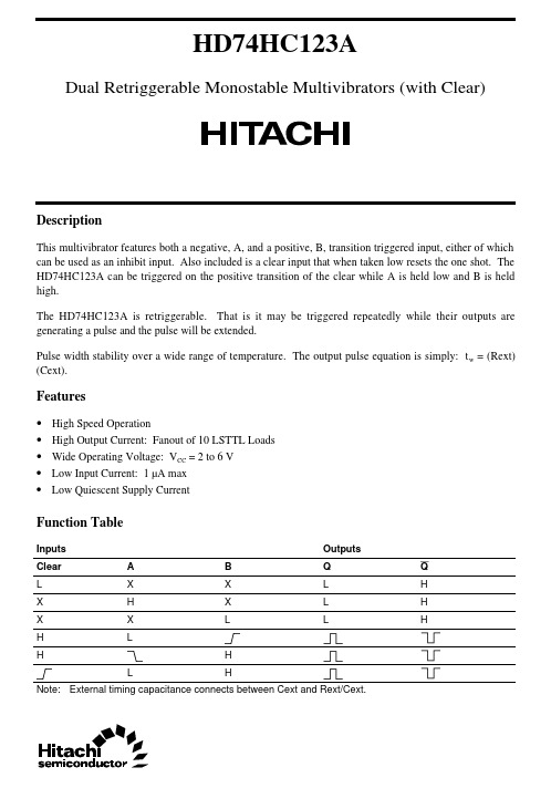
HD74HC123中文资料
DP-16 Conforms Conforms 1.07 g
元器件交易网
10.06
10.5 Max
16
9
5.5
1
8
0.80 Max
2.20 Max
0.10 ± 0.10
1.27
*0.42 ± 0.08 0.40 ± 0.06
0.15 0.12 M
*Dimension including the plating thickness Base material dimension
Output rise time tTLH
2.0
— — 75 — 95 ns
4.5
— 5 15 — 19
6.0
— — 13 — 16
Output fall time tTHL
2.0
— — 75 — 95 ns
4.5
— 5 15 — 19
6.0
— — 13 — 16
Pulse width
tw
2.0
150 — — 190 — ns A, B, Clear
VCC (V) 2.0 4.5
Min Typ Max Min — — 210 — — 22 42 —
Max Unit 265 ns 53
Test Conditions A, B or Clear to Q
6.0
— — 36 — 45
t PHL
2.0
— — 240 — 300 ns A, B or Clear to Q
4.5
— 1.0 — — — ms Cext = 0.1 µF, Rext = 10 kΩ
—
— 5 10 — 10 pF
Caution in use: In order to prevent any malfunctions due to noise, connect a high-frequency performance
HD74HC190中文资料
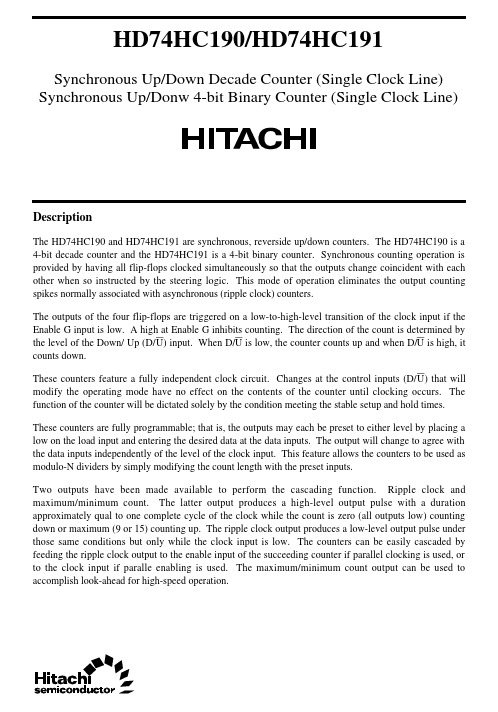
HD74HC190/HD74HC191 Synchronous Up/Down Decade Counter (Single Clock Line) Synchronous Up/Donw 4-bit Binary Counter (Single Clock Line)DescriptionThe HD74HC190 and HD74HC191 are synchronous, reverside up/down counters. The HD74HC190 is a 4-bit decade counter and the HD74HC191 is a 4-bit binary counter. Synchronous counting operation is provided by having all flip-flops clocked simultaneously so that the outputs change coincident with each other when so instructed by the steering logic. This mode of operation eliminates the output counting spikes normally associated with asynchronous (ripple clock) counters.The outputs of the four flip-flops are triggered on a low-to-high-level transition of the clock input if the Enable G input is low. A high at Enable G inhibits counting. The direction of the count is determined by the level of the Down/ Up (D/U) input. When D/U is low, the counter counts up and when D/U is high, it counts down.These counters feature a fully independent clock circuit. Changes at the control inputs (D/U) that will modify the operating mode have no effect on the contents of the counter until clocking occurs. The function of the counter will be dictated solely by the condition meeting the stable setup and hold times. These counters are fully programmable; that is, the outputs may each be preset to either level by placing a low on the load input and entering the desired data at the data inputs. The output will change to agree with the data inputs independently of the level of the clock input. This feature allows the counters to be used as modulo-N dividers by simply modifying the count length with the preset inputs.Two outputs have been made available to perform the cascading function. Ripple clock and maximum/minimum count. The latter output produces a high-level output pulse with a duration approximately qual to one complete cycle of the clock while the count is zero (all outputs low) counting down or maximum (9 or 15) counting up. The ripple clock output produces a low-level output pulse under those same conditions but only while the clock input is low. The counters can be easily cascaded by feeding the ripple clock output to the enable input of the succeeding counter if parallel clocking is used, or to the clock input if paralle enabling is used. The maximum/minimum count output can be used to accomplish look-ahead for high-speed operation.HD74HC190/HD74HC191Features• High Speed Operation: t pd (Clock to Q) = 22 ns typ (C L = 50 pF)• High Output Current: Fanout of 10 LSTTL Loads• Wide Operating Voltage: V CC = 2 to 6 V• Low Input Current: 1 µA max• Low Quiescent Supply Current: I CC (static) = 4 µA max (Ta = 25°C) Pin Arrangement2HD74HC190/HD74HC191 Timing ChartHD74HC190Illustrated below is the following sequence:1.Load (preset) to BCD seven.2.Count up to eight, nine (maximum), zero, one and two.3.Inhibit4.Count down to one, zero (minimum), nine, eight and seven.3HD74HC190/HD74HC191HD74HC191Illustrated below is the following sequence:1.Load (preset) to binary thirteen.2.Count up to fourteen, fifteen (maximum), zero, one and two.3.Inhibit4.Count down to one, zero (minimum), fifteen, fourteen and thirteen.4HD74HC190/HD74HC191 Logic DiagramHD74HC1905HD74HC190/HD74HC191 HD74HC1916HD74HC190/HD74HC1917DC CharacteristicsTa = 25°CTa = –40 to +85°CItem Symbol V CC (V)Min Typ Max MinMax Unit Test ConditionsInput voltageV IH2.0 1.5—— 1.5—V4.5 3.15—— 3.15—6.04.2—— 4.2—V IL2.0——0.5—0.5V 4.5—— 1.35—1.356.0——1.8— 1.8Output voltageV OH2.0 1.9 2.0— 1.9—VVin = V IH or V IL I OH = –20 µA4.5 4.4 4.5— 4.4—6.05.96.0— 5.9—4.5 4.18—— 4.13—I OH = –4 mA 6.05.68——5.63—I OH = –5.2 mAV OL2.0—0.00.1—0.1VVin = V IH or V IL I OL = 20 µA4.5—0.00.1—0.16.0—0.00.1—0.14.5——0.26—0.33I OL = 4 mA 6.0——0.26—0.33I OL = 5.2 mAInput current Iin 6.0——±0.1—±1.0µA Vin = V CC or GNDQuiescent supply currentI CC6.0——4.0—40µAVin = V CC or GND, Iout = 0 µAHD74HC190/HD74HC1918AC Characteristics (C L = 50 pF, Input t r = t f = 6 ns)Ta = 25°CTa = –40 to +85°CItemSymbol V CC (V)Min Typ Max MinMax Unit Test ConditionsMaximum clock f max2.0——5—4MHzfrequency4.5——25—206.0——29—24Propagation delay t PLH 2.0——265—335nsLoad to Qtimet PHL 4.5—2153—666.0——45—562.0——230—290Data to Q4.5—1846—586.0——39—492.0——120—150Clock to RC 4.5—1424—306.0——20—262.0——190—240Clock to Q 4.5—2238—486.0——32—412.0——250—315Clock to max/min 4.5—2650—636.0——43—542.0——230—290Down/up to RC 4.5—2046—586.0——39—492.0——130—165G to RC 4.5—1426—336.0——22—282.0——190—240Down/up to max/min 4.5—1738—486.0——32—41Pulse widtht w2.080——100—ns4.5168—20—6.014–—17—Hold timet h2.00——0—ns 4.50–6—0—6.0———HD74HC190/HD74HC1919AC Characteristics (C L = 50 pF, Input t r = t f = 6 ns) (cont)Ta = 25°CTa = –40 to +85°CItem Symbol V CC (V)Min Typ Max MinMax Unit Test ConditionsSetup timet su2.0100——125—ns4.5207—25—6.017——21—Output rise/fall t TLH 2.0——75—95ns timet THL 4.5—515—196.0——13—16Input capacitanceCin——510—10pFHitachi CodeJEDECEIAJWeight (reference value)DP-16ConformsConforms1.07 gUnit: mmHitachi Code JEDEC FP-16DA —Unit: mm° – 8°元器件交易网Hitachi Code JEDEC FP-16DNConformsUnit: mm° – 8°元器件交易网Cautions1.Hitachi neither warrants nor grants licenses of any rights of Hitachi’s or any third party’s patent,copyright, trademark, or other intellectual property rights for information contained in this document.Hitachi bears no responsibility for problems that may arise with third party’s rights, includingintellectual property rights, in connection with use of the information contained in this document.2.Products and product specifications may be subject to change without notice. Confirm that you have received the latest product standards or specifications before final design, purchase or use.3.Hitachi makes every attempt to ensure that its products are of high quality and reliability. However,contact Hitachi’s sales office before using the product in an application that demands especially high quality and reliability or where its failure or malfunction may directly threaten human life or cause risk of bodily injury, such as aerospace, aeronautics, nuclear power, combustion control, transportation,traffic, safety equipment or medical equipment for life support.4.Design your application so that the product is used within the ranges guaranteed by Hitachi particularly for maximum rating, operating supply voltage range, heat radiation characteristics, installationconditions and other characteristics. Hitachi bears no responsibility for failure or damage when used beyond the guaranteed ranges. Even within the guaranteed ranges, consider normally foreseeable failure rates or failure modes in semiconductor devices and employ systemic measures such as fail-safes, so that the equipment incorporating Hitachi product does not cause bodily injury, fire or other consequential damage due to operation of the Hitachi product.5.This product is not designed to be radiation resistant.6.No one is permitted to reproduce or duplicate, in any form, the whole or part of this document without written approval from Hitachi.7.Contact Hitachi’s sales office for any questions regarding this document or Hitachi semiconductor products.Hitachi, Ltd.Semiconductor & Integrated Circuits.Nippon Bldg., 2-6-2, Ohte-machi, Chiyoda-ku, Tokyo 100-0004, Japan Tel: Tokyo (03) 3270-2111 Fax: (03) 3270-5109Copyright ' Hitachi, Ltd., 1999. All rights reserved. Printed in Japan.Hitachi Asia Pte. Ltd.16 Collyer Quay #20-00Hitachi TowerSingapore 049318Tel: 535-2100Fax: 535-1533URLNorthAmerica : http:/Europe : /hel/ecg Asia (Singapore): .sg/grp3/sicd/index.htm Asia (Taiwan): /E/Product/SICD_Frame.htm Asia (HongKong): /eng/bo/grp3/index.htm Japan : http://www.hitachi.co.jp/Sicd/indx.htmHitachi Asia Ltd.Taipei Branch Office3F, Hung Kuo Building. No.167, Tun-Hwa North Road, Taipei (105)Tel: <886> (2) 2718-3666Fax: <886> (2) 2718-8180Hitachi Asia (Hong Kong) Ltd.Group III (Electronic Components)7/F., North Tower, World Finance Centre,Harbour City, Canton Road, Tsim Sha Tsui,Kowloon, Hong Kong Tel: <852> (2) 735 9218Fax: <852> (2) 730 0281 Telex: 40815 HITEC HXHitachi Europe Ltd.Electronic Components Group.Whitebrook ParkLower Cookham Road MaidenheadBerkshire SL6 8YA, United Kingdom Tel: <44> (1628) 585000Fax: <44> (1628) 778322Hitachi Europe GmbHElectronic components Group Dornacher Stra§e 3D-85622 Feldkirchen, Munich GermanyTel: <49> (89) 9 9180-0Fax: <49> (89) 9 29 30 00Hitachi Semiconductor (America) Inc.179 East Tasman Drive,San Jose,CA 95134 Tel: <1> (408) 433-1990Fax: <1>(408) 433-0223For further information write to:。
- 1、下载文档前请自行甄别文档内容的完整性,平台不提供额外的编辑、内容补充、找答案等附加服务。
- 2、"仅部分预览"的文档,不可在线预览部分如存在完整性等问题,可反馈申请退款(可完整预览的文档不适用该条件!)。
- 3、如文档侵犯您的权益,请联系客服反馈,我们会尽快为您处理(人工客服工作时间:9:00-18:30)。
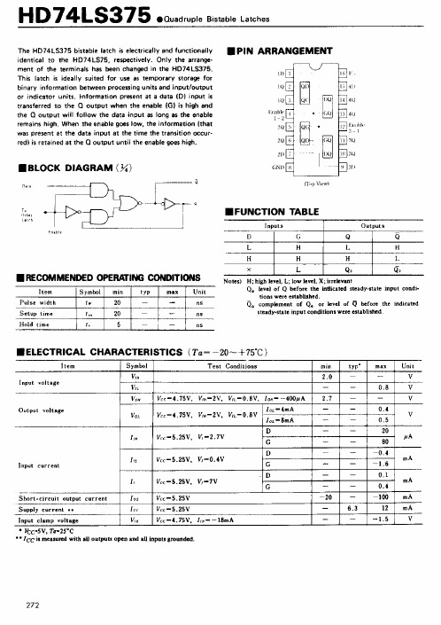
HD74HC375Quad. Bistable LatchesADE-205-500 (Z)1st. EditionSep. 2000 DescriptionThis latch is ideally suited for use as temporary storage for binary information between processing units and input/output or indicator units. Information present at a data (D) input is transferred to the Q output when the enable (G) is high and the Q output will follow the data input as long as the enable remains high. When the enable goes low, the information (that was present at the data input at the time the transition occurred) is retained at the Q output until the enable goes high.Features• High Speed Operation: t pd (Data to Q, Q) = 10 ns typ (C L = 50 pF)• High Output Current: Fanout of 10 LSTTL Loads• Wide Operating Voltage: V CC = 2 to 6 V• Low Input Current: 1 µA max• Low Quiescent Supply Current: I CC (static) = 4 µA max (Ta = 25°C)Function TableInputs OutputsD G Q QL H L HH H H LX L no change no changeHD74HC375 Pin Arrangement2HD74HC3753DC CharacteristicsTa = 25°CTa = –40 to +85°CItem Symbol V CC (V)Min Typ Max MinMax Unit Test ConditionsInput voltageV IH2.0 1.5—— 1.5—V4.5 3.15—— 3.15—6.04.2—— 4.2—V IL2.0——0.5—0.5V 4.5—— 1.35—1.356.0——1.8— 1.8Output voltageV OH2.0 1.9 2.0— 1.9—VVin = V IH or V IL I OH = –20 µA4.5 4.4 4.5— 4.4—6.05.96.0— 5.9—4.5 4.18—— 4.13—I OH = –4 mA 6.05.68——5.63—I OH = –5.2 mAV OL2.0—0.00.1—0.1VVin = V IH or V IL I OL = 20 µA4.5—0.00.1—0.16.0—0.00.1—0.14.5——0.26—0.33I OL = 4 mA 6.0——0.26—0.33I OL = 5.2 mAInput current Iin 6.0——±0.1—±1.0µA Vin = V CC or GNDQuiescent supply currentI CC6.0——4.0—40µAVin = V CC or GND, Iout = 0 µAHD74HC3754AC Characteristics (C L = 50 pF, Input t r = t f = 6 ns)Ta = 25°CTa = –40 to +85°CItem Symbol V CC (V)Min Typ Max MinMax Unit Test Conditions Propagation delay t PLH2.0——145—180nsData to Q or Qtimet PHL 4.5—1029—366.0——25—31t PLH 2.0——160—200nsG to Q or Qt PHL4.5—1132—406.0——27—34Pulse widtht w2.080——100—ns 4.5165—20—6.014——17—Setup timet su2.0100——125—ns 4.5202—25—6.017——21—Hold timet h2.05——5—ns 4.55–1—5—6.05——5—Output rise/fall t TLH 2.0——75—95ns timet THL 4.5—515—196.0——13—16Input capacitanceCin——510—10pFHD74HC375 Package Dimensions5HD74HC3756HD74HC3757Cautions1.Hitachi neither warrants nor grants licenses of any rights of Hitachi’s or any third party’s patent,copyright, trademark, or other intellectual property rights for information contained in this document.Hitachi bears no responsibility for problems that may arise with third party’s rights, includingintellectual property rights, in connection with use of the information contained in this document.2.Products and product specifications may be subject to change without notice. Confirm that you have received the latest product standards or specifications before final design, purchase or use.3.Hitachi makes every attempt to ensure that its products are of high quality and reliability. However,contact Hitachi’s sales office before using the product in an application that demands especially high quality and reliability or where its failure or malfunction may directly threaten human life or cause risk of bodily injury, such as aerospace, aeronautics, nuclear power, combustion control, transportation,traffic, safety equipment or medical equipment for life support.4.Design your application so that the product is used within the ranges guaranteed by Hitachi particularly for maximum rating, operating supply voltage range, heat radiation characteristics, installationconditions and other characteristics. Hitachi bears no responsibility for failure or damage when used beyond the guaranteed ranges. Even within the guaranteed ranges, consider normally foreseeable failure rates or failure modes in semiconductor devices and employ systemic measures such as fail-safes, so that the equipment incorporating Hitachi product does not cause bodily injury, fire or other consequential damage due to operation of the Hitachi product.5.This product is not designed to be radiation resistant.6.No one is permitted to reproduce or duplicate, in any form, the whole or part of this document without written approval from Hitachi.7.Contact Hitachi’s sales office for any questions regarding this document or Hitachi semiconductor products.Hitachi, Ltd.Semiconductor & Integrated Circuits.Nippon Bldg., 2-6-2, Ohte-machi, Chiyoda-ku, Tokyo 100-0004, Japan Tel: Tokyo (03) 3270-2111 Fax: (03) 3270-5109Copyright © Hitachi, Ltd., 2000. All rights reserved. Printed in Japan.Hitachi Asia Ltd. Hitachi Tower16 Collyer Quay #20-00, Singapore 049318Tel : <65>-538-6533/538-8577 Fax : <65>-538-6933/538-3877URL : .sg URLNorthAmerica : /Europe : /hel/ecg Asia : Japan : http://www.hitachi.co.jp/Sicd/indx.htmHitachi Asia Ltd.(Taipei Branch Office)4/F, No. 167, Tun Hwa North Road, Hung-Kuo Building, Taipei (105), Taiwan Tel : <886>-(2)-2718-3666 Fax : <886>-(2)-2718-8180 Telex : 23222 HAS-TPURL : Hitachi Asia (Hong Kong) Ltd. Group III (Electronic Components) 7/F., North Tower, World Finance Centre,Harbour City, Canton Road Tsim Sha Tsui, Kowloon, Hong KongTel : <852>-(2)-735-9218 Fax : <852>-(2)-730-0281URL : Hitachi Europe Ltd.Electronic Components Group.Whitebrook ParkLower Cookham Road MaidenheadBerkshire SL6 8YA, United Kingdom Tel: <44> (1628) 585000Fax: <44> (1628) 585160Hitachi Europe GmbHElectronic Components Group Dornacher Stra βe 3D-85622 Feldkirchen, Munich GermanyTel: <49> (89) 9 9180-0Fax: <49> (89) 9 29 30 00Hitachi Semiconductor (America) Inc.179 East Tasman Drive,San Jose,CA 95134 Tel: <1> (408) 433-1990Fax: <1>(408) 433-0223For further information write to:Colophon 2.0。