Spectral interferometric optical coherence tomography with nonlinear b-barium borate time g
现代材料分析方法(英文)
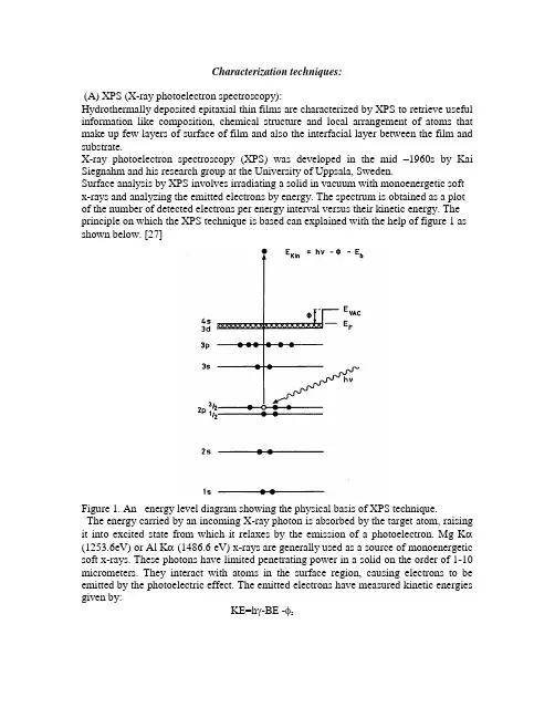
Characterization techniques:(A) XPS (X-ray photoelectron spectroscopy):Hydrothermally deposited epitaxial thin films are characterized by XPS to retrieve useful information like composition, chemical structure and local arrangement of atoms that make up few layers of surface of film and also the interfacial layer between the film and substrate.X-ray photoelectron spectroscopy (XPS) was developed in the mid –1960s by Kai Siegnahm and his research group at the University of Uppsala, Sweden.Surface analysis by XPS involves irradiating a solid in vacuum with monoenergetic soft x-rays and analyzing the emitted electrons by energy. The spectrum is obtained as a plot of the number of detected electrons per energy interval versus their kinetic energy. The principle on which the XPS technique is based can explained with the help of figure 1 as shown below. [27]Figure 1. An energy level diagram showing the physical basis of XPS technique.The energy carried by an incoming X-ray photon is absorbed by the target atom, raising it into excited state from which it relaxes by the emission of a photoelectron. Mg Kα(1253.6eV) or Al Kα (1486.6 eV) x-rays are generally used as a source of monoenergetic soft x-rays. These photons have limited penetrating power in a solid on the order of 1-10 micrometers. They interact with atoms in the surface region, causing electrons to be emitted by the photoelectric effect. The emitted electrons have measured kinetic energies given by:KE=hγ-BE -φsWhere hγ is the energy of the photon, BE is the binding energy of the atomic orbital from which the electron originates and φs is the spectrometer work function. The binding energy may be regarded as the energy difference between the initial and final states after the photoelectron has left the atom. Because there are a variety of possible final states of the ions from each type of atom, there is corresponding variety of kinetic energies of the emitted electrons. Photoelectrons are emitted from all energy levels of the target atom and hence the electron energy spectrum is characteristic of the emitting atom type and may be thought as its XPS fingerprint. Each element has unique spectrum .The spectrum from a mixture of elements is approximately the sum of peaks of the individual constituents. Because the mean free path of electrons in the solids is very small, the detected electrons originate from only the top few atomic layers making XPS a unique surface sensitive technique for chemical analysis. Quantitative data can be obtained from peak heights or peak areas and identification of chemical states often can be made from exact measurement of peak positions and separations as well from certain spectral features.The line lengths indicate the relative probabilities of the various ionization processes. The p,d and f levels split upon ionization leading to vacancies in the p1/2,p3/2,d3/2,d5/2,f5/2 and f7/2.The spin orbit splitting ratio is 1:2 for p levels ,2:3 for d levels and 3:4 for f levels .Because each element has a unique set of binding energies, XPS can be used to identify and determine the concentration of the elements in the surface. Variations in the elemental binding energies (the chemical shifts) arise from the differences in the chemical potential and polarizibilty of compounds. These chemical shifts can be analyzed to identify the chemical state of the materials being analyzed.The electrons leaving sample are detected by an electron spectrometer according to their kinetic energy. The analyzer is usually operated as an energy window, referred to as pass energy. To maintain a constant energy resolution, the pass energy is fixed. Incoming electrons are adjusted the pass energy before entering the energy analyzer. Scanning for different energies is accomplished by applying a variable electrostatic field before the analyzer. This retardation voltage may be varied from zero upto and beyond the photon energy. Electrons are detected as discrete events, and the number of electrons for the given detection time. And energy is stored and displayed.In general, the interpretation of the XPS spectrum is most readily accomplished first by identifying the lines that almost always present (specifically those of C and O), then by identifying major lines and associated weaker lines.(B) Auger electron spectroscopy:Auger electron spectroscopy is a very useful technique in elemental characterization of thin films. In the current project this technique has been utilized not only for elemental compositional analysis but also for understanding nucleation and growth mechanism. Auger electron effect is named after the French physicist Pierre Auger who described the process involved in 1925.Auger is process is bit more complicated than the XPS process.The Auger process occurs in three stages. First one being atomic ionization. Second being electron emission (Auger emission) and third being analysis of emitted auger electrons .The source of radiation used is electrons that strike in the range of 2 to 10 kev. The interatomic process resulting in the production of an Auger electron is shown in figure 2 below.Figure 2 showing the interatomic process resulting in production of the Auger electrons. One electron falls a higher level to fill an initial core hole in the k-shell and the energy liberated in this process is given to second electron ,fraction of this energy is retained by auger electron as kinetic energy.X-ray nomenclature is used for the energy levels involved and the auger electron is described as originating from for example ,an ABC auger transition where A is the level of the original core hole,B is the level from which core hole was filled and C is the level from which auger electron was emitted. In above figure 2 shown above the auger transition is described as L3M1M2, 3.The calculation of energies of the lines in the Auger electron spectrum is complicated by the fact that emission occurs from an atom in an excited state and consequently the energies of the levels involved are difficult to define precisely.Each element in a sample being studied gives rise to characteristic spectrum of peaks at various kinetic energies. Area generally scanned is 1 mm2.To understand the variation in the concentration with the distance from the surface depth profiling can also be carried out. For depth profiling the surface has to be etched away by using argon beam.The principle advantage that AES hold over XPS is that the source of excitation in case of AES is electrons which allows it to take a spectra from micro-regions as small as 100 nm diameters or less instead of averaging over the whole of the surface of the sample as is done generally in XPS.(C) Atomic force Microscope:Atomic Force Microscope (AFM ) is being used to solve processing and materials problems in a wide range of technologies affecting the electronics, telecommunications, biological, chemical, automotive, aerospace, and energy industries. The materials being investigating include thin and thick film coatings, ceramics, composites, glasses, synthetic and biological membranes, metals, polymers, and semiconductors.In the current work AFM was used to understand the nucleation and growth mechanism of the epitaxial thin films and to understand the surface morphology of totally grown films in terms of surface coverage and surface roughness.In the fall of 1985 Gerd Binnig and Christoph Gerber used the cantilever to examine insulating surfaces. A small hook at the end of the cantilever was pressed against the surface while the sample was scanned beneath the tip. The force between tip and sample was measured by tracking the deflection of the cantilever. This was done by monitoring the tunneling current to a second tip positioned above the cantilever. They were able to delineate lateral features as small as 300 Å. This is the way force microscope was developed. Albrecht, a fresh graduate student, who fabricated the first silicon microcantilever and measured the atomic structure of boron nitride. The tip-cantilever assembly typically is microfabricated from Si or Si3N4. The force between the tip and the sample surface is very small, usually less than 10-9 N.According to the interaction of the tip and the sample surface, the AFM is classified as repulsive or Contact mode and attractive or Noncontact mode. In contact mode the topography is measured by sliding the probe tip across the sample surface. In noncontact mode, topography is measured by sensing Van de Waals forces between the surface and probe tip. Held above the surface. The tapping mode which has now become more popular measures topography by tapping the surface with an oscillating probe tip which eliminates shear forces which can damage soft samples and reduce image resolution. 1. Laser2. Mirror3. Photo detector4. Amplifier5. Register6. Sample7. Probe8. CantileverFigure 3 showing a schematic diagram of the principle of AFM.Compared with Optical Interferometric Microscope (optical profiles), the AFM provides unambiguous measurement of step heights, independent of reflectivity differences between materials. Compared with Scanning Electron Microscope, AFM provides extraordinary topographic contrast direct height measurements and unobscured views of surface features (no coating is necessary). One of the advantages of the technique being that it can be applied to insulating samples as well. Compared with Transmission Electron Microscopes, three dimensional AFM images are obtained without expensive sample preparation and yield far more complete information than the two dimensional profiles available from cross-sectioned samples.(D) Fourier Transform Infrared Spectroscopy:Infrared spectroscopy is widely used chemical analysis tool which in addition to providing information on chemical structures also can give quantitative information such as concentration of molecules in a sample.The development in FTIR started with use of Michelson interferometer an optical device invented in 1880 by Albert Abraham Michelson. After many years of difficultiesin working out with time consuming calculations required for conversion intereferogram into spectrum, the first FTIR was manufactured by the Digilab in Cambridge Massachusetts in 1960s .These FTIR machines stared using computers for calculating fourier transforms faster.The set up consists of a source, a sample and a detector and it is possible to send all the source energy through an interferometer and onto the sample. In every scan, all source radiation gets to the sample. The interferometer is a fundamentally different piece of equipment than a monochromater. The light passes through a beamsplitter, which sends the light in two directions at right angles. One beam goes to a stationary mirror then back to the beamsplitter. The other goes to a moving mirror. The motion of the mirror makes the total path length variable versus that taken by the stationary-mirror beam. When the two meet up again at the beamsplitter, they recombine, but the difference in path lengths creates constructive and destructive interference: an interferogram:The recombined beam passes through the sample. The sample absorbs all the different wavelengths characteristic of its spectrum, and this subtracts specific wavelengths from the interferogram. The detector reports variation in energy versus time for all wavelengths simultaneously. A laser beam is superimposed to provide a reference for the instrument operation.Energy versus time was an odd way to record a spectrum, until the point it was recognized that there is reciprocal relationship between time and frequency. A Fourier transform allows to convert an intensity-vs.-time spectrum into an intensity-vs.-frequency spectrum.The advantages of FTIR are that all of the source energy gets to the sample, improving the inherent signal-to-noise ratio. Resolution is limited by the design of the interferometer. The longer the path of the moving mirror, the higher the resolution.One minor drawback is that the FT instrument is inherently a single-beam instrument and the result is that IR-active atmospheric components (CO2, H2O) appear in the spectrum. Usually, a "Background" spectrum is run, and then automatically subtracted from every spectrum.(E) Scanning Electron Microscopy:Scanning electron microscopy is one the most versatile characterization techniques that can give detailed information interms of topography, morphology, composition and crystallography. This has made it widely useful in thin film characterization.The scanning electron microscope is similar to its optical counterparts except that it uses focused beam of electrons instead of light to image the specimen to gain information about the structure and composition.A stream electron is accelerated towards positive electrical potential. This stream is confined and focused using metal apertures and magnetic lenses into a thin, focused, monochromatic beam. This beam is focused onto the sample using a magnetic lens. Interactions occur inside the irradiated sample, affecting the electron beam. These interactions and effects are detected and transformed into an image. The electron detector collects the electrons and then image is created. Scanning with SEM is accomplished bytwo pairs of electromagnetic coils located within the objective lens, one pair deflects the beam in x-direction across the sample and the other pair deflects it in the y direction. Scanning is controlled by applying an electric signal to one pair of scan coils such that the electron beam strikes the sample to one side of theFigure 4 Schematic view of a SEM instrument.center axis of the lens system. By varying the electrical signal to this pair of coils as a function of time, the electron beam is moved in a straight line across the sample and then returned to its original position. Thus by rapidly moving the beam the entire sample surface can be irradiated with the electron beam. The output signal consists of backscattered and secondary electrons which generally serve as basis of scanning electron microscope and whereas the x-ray emission serves as the basis of the energy dispersive spectroscopy as shown in figure 4.Figure 5.Schematic presentation of the interaction of the electron with the sample.Energy dispersive spectroscopy is analytical method which is used in determination of elemental composition of the specimen.EDS uses the electrons generated characteristic x-radiation to determine elemental composition. The SEM/EDS combination is a powerful tool in inorganic microanalysis, providing the chemical composition of volumes as small as 3 m3.(F) Transmission Electron microscopy:Transmission electron microscopy was used to analyze the interface between the BaTiO3 on SrTiO3 single crystals.For TEM specimen must be specially prepared to thicknesses which allow electrons to transmit through the sample, much like light is transmitted through materials in conventional optical microscopy. Because the wavelength of electrons is much smaller than that of light, the optimal resolution attainable for TEM images is many orders of magnitude better than that from a light microscope. Thus, TEMs can reveal the finest details of internal structure - in some cases as small as individual atoms. Magnifications of 350,000 times can be routinely obtained for many materials, whilst in special circumstances; atoms can be imaged at magnifications greater than 15 million timesThe energy of the electrons in the TEM determine the relative degree of penetration of electrons in a specific sample, or alternatively, influence the thickness of material from which useful information may be obtained.Cross-sectional specimens for TEM observation of the interface between the film and the substrate were prepared by conventional techniques employing mechanical polishing, dimpling and ion beam milling.TEM column is shown in figure 6 consists of gun chamber on the top to the camera at the bottom everything is placed under vacuum.Figure 6. Main components of TEM system. [28]At the top of the TEM column is the filament assembly, which is connected to thehigh voltage supply by insulated cable. In standard TEM, normal accelerating voltagesranges from 20,000 to 100,000V.Intermediate-voltage and high voltage TEMs may use accelerating voltages of 200,000 V to 1000000 V.The higher the accelerating voltage, the greater the theoretical resolution. Below the filament tip and above it the anode is a beam volume called crossover. In this area of the filament chamber, the electron beam volume iscondensed to its highest density. There are more electrons per unit area at the cross over than at any other place in the microscope. Crossover is the effective electron source for image formation. In a TEM, the diameter of the electron beam at crossover is approximately 50 μm.The anode or positively charged plate, is below the filament assembly.Electron beam then travels to the condenser –lens system.TEMs has two condensers lenses. Condenser system lens system controls electron illumination on the specimen and on the viewing screen for such functions as viewing, focusing and photography. Condenserlenses are fitted with apertures which are usually small platinum disks or molybdenum strips with holes of various sizes ranging from 100 to 400 μm and it protects specimen from too many stray electrons which can contribute to excessive heat and limit X-ray production farther down the columnObjective lens is the first magnifying lens and the specimen is inserted into the objective lens, which must be designed so that the specimen can be moved in both X and Y directions and have tilting and rotating capabilities. As the electron beam interacts with the specimen, a number of signals useful in the formation of the TEM image occur: absorption, diffraction, elastic scattering and inelastic scattering.(H) X-ray Diffraction (XRD):X-ray diffraction is the most commonly known technique which I used to determination of the phase formed in films and also to assess texture and crystallinity.X-rays were discovered in 1895 by the German physicist Wilhelm Conrad Röntgen - in some languages x-rays are called Röntgen-rays - and x-ray diffraction was discovered in 1912.The X-rays used in diffraction experiments all have a wavelength of 0.5-2.5 Å. The intensity of a beam of x-rays is the rate of transport of energy flow through a unit area perpendicular to the direction of propagation. To produce x-rays, a source of electrons, a high accelerating voltage and a target are needed. To get the voltage, the metal target is grounded and a cathode is at 30-50 kV. To get the electrons a metal filament is resistively heated (the tube is called a filament tube). The filament current is 3-5 amps. The cathode and the filament is one and the same thing and surrounding the target and the filament is an air evacuated envelope.The electrons from the filament are accelerated towards the target. They bombard the target in a rectangular shaped area called the focal spot. From there the x-rays are emitted in all directions. The walls of the tube are impenetrable for the x-rays except where beryllium windows are inserted. Beryllium has a very low absorption coefficient for the x-rays.The amount of x-rays produced depends on the number of electrons emitted and their energy when they reach the target. The number of electrons in turn depends on the filament temperature, and thus the filament current. The current of electrons from the filament to the target is measurable and usually 25-55 mA. This current can be chosen freely as a feedback loop will feed the filament with the current needed. The energy ofthe electrons depend on the accelerating voltage. Thus the total intensity emitted by thex-ray tube depends on both the operating voltage and the tube current.In general, diffraction is possible when the length of the wave is of the same order of magnitude as the distance between the regularly spaced scattering objectsTwo scattered rays are in phase, if their path difference is equal to a whole number n of wavelengths. Scattered rays emerging from a plane surface as a result of a beam incident on that surface, have a path difference equal to a whole number of wavelengths, if n l = 2 d' sinq (The Bragg Law),where d' is the distance between the diffracting planes in the crystal and q is the angle between the incident beam and the surface. n is the order of reflection and n can be any integral number as long as sin q < 1. n is also equal to the number of wavelengths in the path difference of two rays scattered from adjacent planes (e.g. If n = 2 then a ray scattered from one plane will have a path that is two wavelengths shorter than a ray scattered from a deeper lying neighbor plane).The basis for phase analysis is that the crystal of a certain phase will have interatomic distances peculiar to that phase and these different distances will cause a series of reflections as the detector are shifted through 2theta.Two phases can have similar or almost similar structures and hence interatomic distances. This makes identifying phases in an unknown sample very difficult, but knowing what elements are present in the sample will narrow the possibilities down quite a bit. Also crystallite size using XRD .X-ray pole figure measurements are used to characterize the film with respect to any preferred orientation with which growth has taken place. Rocking curve is another application to characterize the film with respect to its quality ofcrystallinity comparing to the single crystals or polycrystalline materials.。
光电技术专业英语词汇
《光电技术》专业英语词汇1.Absorption coefficient 吸收系数2.Acceptance angle 接收角3.fibers 光纤4.Acceptors in semiconductors 半导体接收器5.Acousto-optic modulator 声光调制6.Bragg diffraction 布拉格衍射7.Air disk 艾里斑8.angular radius 角半径9.Airy rings 艾里环10.anisotropy 各向异性11.optical 光学的12.refractive index 各向异性13.Antireflection coating 抗反膜14.Argon-ion laser 氩离子激光器15.Attenuation coefficient 衰减系数16.Avalanche 雪崩17.breakdown voltage 击穿电压18.multiplication factor 倍增因子19.noise 燥声20.Avalanche photodiode(APD) 雪崩二极管21.absorption region in APD APD 吸收区域22.characteristics-table 特性表格23.guard ring 保护环24.internal gain 内增益25.noise 噪声26.photogeneration 光子再生27.primary photocurrent 起始光电流28.principle 原理29.responsivity of InGaAs InGaAs 响应度30.separate absorption and multiplication(SAM) 分离吸收和倍增31.separate absorption grading and multiplication(SAGM) 分离吸收等级和倍增32.silicon 硅33.Average irradiance 平均照度34.Bandgap 带隙35.energy gap 能级带隙36.bandgap diagram 带隙图37.Bandwidth 带宽38.Beam 光束39.Beam splitter cube 立方分束器40.Biaxial crystal双s 轴晶体41.Birefringent 双折射42.Bit rate 位率43.Black body radiation law 黑体辐射法则44.Bloch wave in a crystal 晶体中布洛赫波45.Boundary conditions 边界条件46.Bragg angle 布拉格角度47.Bragg diffraction condition 布拉格衍射条件48.Bragg wavelength 布拉格波长49.Brewster angle 布鲁斯特角50.Brewster window 布鲁斯特窗51.Calcite 霰石52.Carrier confinement 载流子限制53.Centrosymmetric crystals 中心对称晶体54.Chirping 啁啾55.Cladding 覆层56.Coefficient of index grating 指数光栅系数57.Coherence连贯性pensation doping 掺杂补偿59.Conduction band 导带60.Conductivity 导电性61.Confining layers 限制层62.Conjugate image 共轭像63.Cut-off wavelength 截止波长64.Degenerate semiconductor 简并半导体65.Density of states 态密度66.Depletion layer 耗尽层67.Detectivity 探测率68.Dielectric mirrors 介电质镜像69.Diffraction 衍射70.Diffraction g rating 衍射光栅71.Diffraction grating equation 衍射光栅等式72.Diffusion current 扩散电流73.Diffusion flux 扩散流量74.Diffusion Length 扩散长度75.Diode equation 二极管公式76.Diode ideality factor 二极管理想因子77.Direct recombinatio直n接复合78.Dispersion散射79.Dispersive medium 散射介质80.Distributed Bragg reflector 分布布拉格反射器81.Donors in semiconductors 施主离子82.Doppler broadened linewidth 多普勒扩展线宽83.Doppler effect 多普勒效应84.Doppler shift 多普勒位移85.Doppler-heterostructure 多普勒同质结构86.Drift mobility 漂移迁移率87.Drift Velocity 漂移速度88.Effective d ensity o f s tates 有效态密度89.Effective mass 有效质量90.Efficiency 效率91.Einstein coefficients 爱因斯坦系数92.Electrical bandwidth of fibers 光纤电子带宽93.Electromagnetic wave 电磁波94.Electron affinity 电子亲和势95.Electron potential energy in a crystal 晶体电子阱能量96.Electro-optic effects 光电子效应97.Energy band 能量带宽98.Energy band diagram 能量带宽图99.Energy level 能级100.E pitaxial growth 外延生长101.E rbium doped fiber amplifier 掺饵光纤放大器102.Excess carrier distribution 过剩载流子扩散103.External photocurrent 外部光电流104.Extrinsic semiconductors 本征半导体105.Fabry-Perot laser amplifier 法布里-珀罗激光放大器106.Fabry-Perot optical resonator 法布里-珀罗光谐振器107.Faraday effect 法拉第效应108.Fermi-Dirac function 费米狄拉克结109.Fermi energy 费米能级110.Fill factor 填充因子111.Free spectral range 自由谱范围112.Fresnel’s equations 菲涅耳方程113.Fresnel’s optical indicatrix 菲涅耳椭圆球114.Full width at half maximum 半峰宽115.Full width at half power 半功率带宽116.Gaussian beam 高斯光束117.Gaussian dispersion 高斯散射118.Gaussian pulse 高斯脉冲119.Glass perform 玻璃预制棒120.Goos Haenchen phase shift Goos Haenchen 相位移121.Graded index rod lens 梯度折射率棒透镜122.Group delay 群延迟123.Group velocity 群参数124.Half-wave plate retarder 半波延迟器125.Helium-Neon laser 氦氖激光器126.Heterojunction 异质结127.Heterostructure 异质结构128.Hole 空穴129.Hologram 全息图130.Holography 全息照相131.Homojunction 同质结132.Huygens-Fresnel principle 惠更斯-菲涅耳原理133.Impact-ionization 碰撞电离134.Index matching 指数匹配135.Injection 注射136.Instantaneous irradiance 自发辐射137.Integrated optics 集成光路138.Intensity of light 光强139.Intersymbol interference 符号间干扰140.Intrinsic concentration 本征浓度141.Intrinsic semiconductors 本征半导体142.Irradiance 辐射SER 激光144.active medium 活动介质145.active region 活动区域146.amplifiers 放大器147.cleaved-coupled-cavity 解理耦合腔148.distributed Bragg reflection 分布布拉格反射149.distributed feedback 分布反馈150.efficiency of the He-Ne 氦氖效率151.multiple quantum well 多量子阱152.oscillation condition 振荡条件ser diode 激光二极管sing emission 激光发射155.LED 发光二极管156.Lineshape function 线形结157.Linewidth 线宽158.Lithium niobate 铌酸锂159.Load line 负载线160.Loss c oefficient 损耗系数161.Mazh-Zehnder modulator Mazh-Zehnder 型调制器162.Macrobending loss 宏弯损耗163.Magneto-optic effects 磁光效应164.Magneto-optic isolator 磁光隔离165.Magneto-optic modulator 磁光调制166.Majority carriers 多数载流子167.Matrix emitter 矩阵发射168.Maximum acceptance angle 最优接收角169.Maxwell’s wave equation 麦克斯维方程170.Microbending loss 微弯损耗171.Microlaser 微型激光172.Minority carriers 少数载流子173.Modulated directional coupler 调制定向偶合器174.Modulation of light 光调制175.Monochromatic wave 单色光176.Multiplication region 倍增区177.Negative absolute temperature 负温度系数 round-trip optical gain 环路净光增益179.Noise 噪声180.Noncentrosymmetric crystals 非中心对称晶体181.Nondegenerate semiconductors 非简并半异体182.Non-linear optic 非线性光学183.Non-thermal equilibrium 非热平衡184.Normalized frequency 归一化频率185.Normalized index difference 归一化指数差异186.Normalized propagation constant 归一化传播常数187.Normalized thickness 归一化厚度188.Numerical aperture 孔径189.Optic axis 光轴190.Optical activity 光活性191.Optical anisotropy 光各向异性192.Optical bandwidth 光带宽193.Optical cavity 光腔194.Optical divergence 光发散195.Optic fibers 光纤196.Optical fiber amplifier 光纤放大器197.Optical field 光场198.Optical gain 光增益199.Optical indicatrix 光随圆球200.Optical isolater 光隔离器201.Optical Laser amplifiers 激光放大器202.Optical modulators 光调制器203.Optical pumping 光泵浦204.Opticalresonator 光谐振器205.Optical tunneling光学通道206.Optical isotropic 光学各向同性的207.Outside vapor deposition 管外气相淀积208.Penetration depth 渗透深度209.Phase change 相位改变210.Phase condition in lasers 激光相条件211.Phase matching 相位匹配212.Phase matching angle 相位匹配角213.Phase mismatch 相位失配214.Phase modulation 相位调制215.Phase modulator 相位调制器216.Phase of a wave 波相217.Phase velocity 相速218.Phonon 光子219.Photoconductive detector 光导探测器220.Photoconductive gain 光导增益221.Photoconductivity 光导性222.Photocurrent 光电流223.Photodetector 光探测器224.Photodiode 光电二极管225.Photoelastic effect 光弹效应226.Photogeneration 光子再生227.Photon amplification 光子放大228.Photon confinement 光子限制229.Photortansistor 光电三极管230.Photovoltaic devices 光伏器件231.Piezoelectric effect 压电效应232.Planck’s radiation distribution law 普朗克辐射法则233.Pockels cell modulator 普克尔斯调制器234.Pockel coefficients 普克尔斯系数235.Pockels phase modulator 普克尔斯相位调制器236.Polarization 极化237.Polarization transmission matrix 极化传输矩阵238.Population inversion 粒子数反转239.Poynting vector 能流密度向量240.Preform 预制棒241.Propagation constant 传播常数242.Pumping 泵浦243.Pyroelectric detectors 热释电探测器244.Quantum e fficiency 量子效应245.Quantum noise 量子噪声246.Quantum well 量子阱247.Quarter-wave plate retarder 四分之一波长延迟248.Radiant sensitivity 辐射敏感性249.Ramo’s theorem 拉莫定理250.Rate equations 速率方程251.Rayleigh criterion 瑞利条件252.Rayleigh scattering limit 瑞利散射极限253.Real image 实像254.Recombination 复合255.Recombination lifetime 复合寿命256.Reflectance 反射257.Reflection 反射258.Refracted light 折射光259.Refractive index 折射系数260.Resolving power 分辩力261.Response time 响应时间262.Return-to-zero data rate 归零码263.Rise time 上升时间264.Saturation drift velocity 饱和漂移速度265.Scattering 散射266.Second harmonic generation 二阶谐波267.Self-phase modulation 自相位调制268.Sellmeier dispersion equation 色列米尔波散方程式269.Shockley equation 肖克利公式270.Shot noise 肖特基噪声271.Signal to noise ratio 信噪比272.Single frequency lasers 单波长噪声273.Single quantum well 单量子阱274.Snell’s law 斯涅尔定律275.Solar cell 光电池276.Solid state photomultiplier 固态光复用器277.Spectral intensity 谱强度278.Spectral responsivity 光谱响应279.Spontaneous emission 自发辐射280.stimulated emission 受激辐射281.Terrestrial light 陆地光282.Theraml equilibrium 热平衡283.Thermal generation 热再生284.Thermal velocity 热速度285.Thershold concentration 光强阈值286.Threshold current 阈值电流287.Threshold wavelength 阈值波长288.Total acceptance angle 全接受角289.Totla internal reflection 全反射290.Transfer distance 转移距离291.Transit time 渡越时间292.Transmission coefficient 传输系数293.Tramsmittance 传输294.Transverse electric field 电横波场295.Tranverse magnetic field 磁横波场296.Traveling vave lase 行波激光器297.Uniaxial crystals 单轴晶体298.UnPolarized light 非极化光299.Wave 波300.W ave equation 波公式301.Wavefront 波前302.Waveguide 波导303.Wave n umber 波数304.Wave p acket 波包络305.Wavevector 波矢量306.Dark current 暗电流307.Saturation signal 饱和信号量308.Fringing field drift 边缘电场漂移plementary color 补色310.Image lag 残像311.Charge handling capability 操作电荷量312.Luminous quantity 测光量313.Pixel signal interpolating 插值处理314.Field integration 场读出方式315.Vertical CCD 垂直CCD316.Vertical overflow drain 垂直溢出漏极317.Conduction band 导带318.Charge coupled device 电荷耦合组件319.Electronic shutter 电子快门320.Dynamic range 动态范围321.Temporal resolution 动态分辨率322.Majority carrier 多数载流子323.Amorphous silicon photoconversion layer 非晶硅存储型324.Floating diffusion amplifier 浮置扩散放大器325.Floating gate amplifier 浮置栅极放大器326.Radiant quantity 辐射剂量327.Blooming 高光溢出328.High frame rate readout mode 高速读出模式329.Interlace scan 隔行扫描330.Fixed pattern noise 固定图形噪声331.Photodiode 光电二极管332.Iconoscope 光电摄像管333.Photolelctric effect 光电效应334.Spectral response 光谱响应335.Interline transfer CCD 行间转移型CCD336.Depletion layer 耗尽层plementary metal oxide semi-conductor 互补金属氧化物半导体338.Fundamental absorption edge 基本吸收带339.Valence band 价带340.Transistor 晶体管341.Visible light 可见光342.Spatial filter 空间滤波器343.Block access 块存取344.Pupil compensation 快门校正345.Diffusion current 扩散电流346.Discrete cosine transform 离散余弦变换347.Luminance signal 高度信号348.Quantum efficiency 量子效率349.Smear 漏光350.Edge enhancement 轮廓校正351.Nyquist frequency 奈奎斯特频率352.Energy band 能带353.Bias 偏压354.Drift current 漂移电流355.Clamp 钳位356.Global exposure 全面曝光357.Progressive scan 全像素读出方式358.Full frame CCD 全帧CCD359.Defect correction 缺陷补偿360.Thermal noise 热噪声361.Weak inversion 弱反转362.Shot noise 散粒噪声363.Chrominance difference signal 色差信号364.Colotremperature 色温365.Minority carrier 少数载流子366.Image stabilizer 手振校正367.Horizontal CCD 水平CCD368.Random noise 随机噪声369.Tunneling effect 隧道效应370.Image sensor 图像传感器371.Aliasing 伪信号372.Passive 无源373.Passive pixel sensor 无源像素传感器374.Line transfer 线转移375.Correlated double sampling 相关双采样376.Pinned photodiode 掩埋型光电二极管377.Overflow 溢出378.Effective pixel 有效像素379.Active pixel sensor 有源像素传感器380.Threshold voltage 阈值电压381.Source follower 源极跟随器382.Illuminance 照度383.Refraction index 折射率384.Frame integration 帧读出方式385.Frame interline t ransfer CCD 帧行间转移CCD 386.Frame transfer 帧转移387.Frame transfer CCD 帧转移CCD388.Non interlace 逐行扫描389.Conversion efficiency 转换效率390.Automatic gain control 自动增益控制391.Self-induced drift 自激漂移392.Minimum illumination 最低照度393.CMOS image sensor COMS 图像传感器394.MOS diode MOS 二极管395.MOS image sensor MOS 型图像传感器396.ISO sensitivity ISO 感光度。
tensor傅里叶红外光谱仪仪器参数
tensor傅里叶红外光谱仪仪器参数
傅里叶变换红外光谱仪(Fourier Transform Infrared Spectrometer)是一种常用于分析物质结构和化学成分的仪器。
以下是一些常见的傅里叶变换红外光谱仪的仪器参数:
光源类型:通常使用红外光源,如红外灯或者光纤激光器。
光谱范围:指仪器可以测量的红外光谱范围。
常见的范围包括近红外(NIR,近
于可见光)和中红外(MIR)。
分辨率:表示仪器可以分辨的最小波数差异。
分辨率越高,能够分辨的细微结构和特征越多。
采样方式:可以是透射采样、反射采样或者透射/反射混合采样。
探测器类型:常见的探测器包括硅(Si)探测器、氮化硅(SiN)探测器和铟锗(InGaAs)探测器。
不同的探测器对波段和灵敏度有不同的响应。
数据采集速度:指从样品中采集一次光谱所需的时间。
样品室:为了保持样品稳定和准确地测量,傅里叶变换红外光谱仪通常具有一个样品室或样品台。
附件和选件:仪器可能附带各种选件,如气体流动控制装置、样品温控装置等,以满足不同实验需求。
需要注意的是,具体的傅里叶变换红外光谱仪仪器参数可能因不同品牌、型号和配置而有所差异。
在选择和使用仪器时,应参考具体的仪器说明和使用手册以获取详细的参数和操作指南。
常用仪器英文对照
常用仪器中英文对照原子发射光谱仪Atomic Emission Spectrometer AES电感偶合等离子体发射光谱仪Inductive Coupled Plasma Emission Spectrometer ICP直流等离子体发射光谱仪Direct Current Plasma Emission Spectrometer DCP紫外-可见光分光光度计UV-Visible Spectrophotometer UV-Vis 原子吸收光谱仪Atomic Absorption Spectroscopy荧光光谱仪Fluorescence Spectroscopy傅里叶变换红外光谱仪FT-IR Spectrometer FTIRFourier transform infrared (FT-IR) spectrometer傅里叶变换拉曼光谱仪FT-Raman Spectrometer FTIR-Raman气相色谱仪Gas Chromatograph GC高效液相色谱仪High Performance Liquid Chromatography HPLC凝胶渗透色谱仪Gel Permeation Chromatograph GPCX射线荧光光谱仪X-Ray Fluorescence SpectrometerX射线衍射仪X-Ray Diffractomer XRD广角X射线衍射WAXRD (wide angle)小角X射线散射SAXRS能谱仪Energy Disperse Spectroscopy EDS质谱仪Mass Spectrometer MSICP-质谱联用仪ICP-MS气相色谱-质谱联用仪GC-MS液相色谱-质谱联用仪LC-MS核磁共振波谱仪Nuclear Magnetic Resonance Spectrometer NMR电子显微镜Electro Microscopy扫描电镜scanning electron microscopy SEM透射电镜transmission electron microscopy TEM光学显微镜Optical Microscopy扫描探针显微镜Scanning Probe Microscopy SPM隧道扫描显微镜Scanning Tunneling Microscopy STM原子力显微镜Atomic Force Microscopy AFM物性分析Physical Property Analysis热分析仪Thermal Analyzer微分扫描量热器Differential Scanning Calorimeter DSC热重分析仪thermal gravity analyzerTGA粘度计Viscometer流变仪Rheometer粒度分析仪Particle Size Analyzer离心机Centrifuge超声破碎仪Ultrasonic Cell Disruptor超低温冰箱Ultra-low Temperature Freezer恒温循环泵Constant Temperature Circulator超滤器Ultrahigh Purity Filter冻干机Freeze Drying Equipment紫外检测仪Ultraviolet Detector电解质分析仪Electrolytic Analyzer常用理化仪器对照玻璃漏斗Glass funnel long stem试管test tube ,test tube brush ,test tube holder ,test tube rack 蒸发皿evaporating dish small烧杯beaker量筒grad cylinder洗瓶plastic wash bottle勺皿casserole ,smallstoppered flask分液漏斗separatory funnelwater bath/oil bathstirring barmagnetic stirrer冷凝器condenserBallast bottle圆颈烧瓶Round-buttom flask试剂瓶reagent bottles托盘天平platform balance 台秤0.1g 托盘pan 指针刻度表pointer and scale crossbeams and sliding weights 游码分析天平two-pan/single-pan analytical balance滴定管burette glass bead(basic) nozzle移液管pipette胖肚elongated glass bulb洗耳球rubber suction bulb玻棒glass rod玻璃活塞stopcock容量瓶(volumetric flask比重瓶(one-mark)volumetric flasks胖肚吸管one-mark pipette刻度吸管graduated pipettes实验仪器清单1、柜子中四、抽屉中:锥形瓶(conical flask) 250ml×4 药匙(medicine spoon)×1 (Erlenmeyer flask) 100 ml×3 滴管(drip tube;dropper)×2烧杯(beaker) 500 ml×1 玻棒(Glass stic)×2250 ml×3 木试管夹(test tube clamp;test tube holder)×1容量瓶(volumetric flask) 100 ml×2 乳钵(morta)×150 ml×4 洗耳球(ear washing bulb)碘量瓶(iodineflask) 500 ml×3试剂瓶(reagent bottle) (无色)×2(棕色)×2 配洗液:量筒(cylinder)100 ml×1 K2Cr2O72g+5ml水→65mlH2SO4 (graduated cylinder)10ml×1 边加边搅拌(stir)。
荧光分光光度法英文
荧光分光光度法英文Fluorescence SpectrophotometryFluorescence spectrophotometry is a widely used analytical technique in the fields of chemistry, biology, and medicine. It is based on the emission of light by certain molecules that have been excited by absorbing light of a specific wavelength. This emitted light is known as fluorescence and can be measured by a spectrophotometer.Principles of Fluorescence SpectrophotometryThe basic principle of fluorescence spectrophotometry is the excitation of a molecule by absorbing light at a specific wavelength. The molecule becomes excited and reaches a higher energy state. This energy is released in the form of emitted light at a longer wavelength. The emitted light is detected by a photodetector, and the signal is amplified and recorded by a computer.Advantages of Fluorescence SpectrophotometryFluorescence spectrophotometry has several advantages over other analytical techniques, such as absorbance spectrophotometry. One major advantage is high sensitivity. Fluorescence spectrophotometry can detect trace amounts of substances, which makes it ideal for research and analysis. Another advantage is selectivity. Fluorescence spectrophotometry can selectively measure certain molecules, which makes it useful in identifying specific compounds in a mixture.Applications of Fluorescence SpectrophotometryFluorescence spectrophotometry has numerous applicationsin various scientific fields. It can be used to study the structure and function of biomolecules, such as proteins and nucleic acids. It is also used in the pharmaceutical industry to develop and analyze drugs. In addition, fluorescence spectrophotometry is used in environmental monitoring, food analysis, and forensic science.ConclusionIn conclusion, fluorescence spectrophotometry is a powerful analytical technique that has revolutionized many scientific fields. Its high sensitivity and selectivity make it an indispensable tool in research and analysis. With the development of new instruments and methods, fluorescence spectrophotometry will continue to play an important role in advancing scientific knowledge.。
普雷斯特光谱共焦_概述及解释说明
普雷斯特光谱共焦概述及解释说明1. 引言1.1 概述在现代科学研究中,光谱共焦技术是一种非常重要且强大的工具。
它结合了光学显微镜和光谱分析仪的优点,可以同时实现高分辨率的成像和光谱信息的获取。
普雷斯特光谱共焦技术(Preston spectral confocal)作为一种新型的光谱共焦技术,在生物医学研究和材料科学等领域取得了广泛应用。
1.2 文章结构本文将对普雷斯特光谱共焦进行详细的介绍和解释。
首先,在第2部分中我们将对光谱共焦技术作一个概括性的介绍,包括其定义、发展历程以及应用领域。
之后,在第3部分中我们将详细介绍普雷斯特光谱共焦的原理,其中包括光路设计与光源选择、探测模式及参数设置以及成像过程解析与数据处理。
在第4部分,我们将讨论普雷斯特光谱共焦技术的改进方法并给出应用案例,包括提高空间分辨率方法研究、融合多种光学手段研究样品特性的案例分析以及在生物医学研究中的应用实践。
最后,在第5部分,我们将对普雷斯特光谱共焦技术进行总结与评价,并展望其未来的发展方向和挑战。
1.3 目的本文的目的是为读者提供对普雷斯特光谱共焦技术有一个深入了解的机会。
通过介绍该技术的原理、改进方法和应用实例,读者可以更好地理解该技术在科学研究领域中的作用和意义。
同时,本文还旨在探讨普雷斯特光谱共焦技术未来可能面临的挑战,并对其发展方向进行展望,以促进相关技术的不断创新和进步。
2. 光谱共焦技术概述:2.1 什么是光谱共焦技术光谱共焦技术是一种结合了光学共焦成像和光谱分析的高级显微镜技术。
它允许研究人员在进行成像的同时获取样品的荧光发射或吸收光谱信息。
通过此技术,我们可以获得样品不同位置的荧光发射或吸收特性,从而提供更加全面和准确的信息。
2.2 发展历程随着近年来生命科学领域对于细胞、组织和生物分子研究需求的增加,光谱共焦技术逐渐得到了广泛应用并取得了显著进展。
最初,常规的共焦显微镜只能实现对样品表面进行成像,并无法提供额外的光谱信息。
赛默飞世尔 ARL iSpark 系列光学发射光谱仪 可靠的金属质量 创新的OES 铁和钢
T hermo Scientific ARL iSpark Series Optical Emission SpectrometersThe ARL iSpark Seriesis a high performance OES spectrometer platform based on the best PMT (photomultiplier tube) optics. It features the most sensitive CCD (charge-coupled device) optics, enhanced degree of functionality and other innovative technologies, including:•Unique PMT or dual CCD/PMT optics • Revolutionary digital spark generator • Innovative spark stand design• Advanced acquisition technologies and processing algorithms for PMT and CCD signals• Single Spark Acquisition with diffuse spark intensity removal algorithm to improve accuracy on PMTs • Most advanced analysis of micro-inclusions• Smart argon management with argon saving modesSpark optical emission spectrometry (OES)is the most widely used technique for elemental concentration analysis of solid metallic samples. With industry leading quality and performance, Thermo Scientific OES spectrometers excel in every aspect of this process with:•Very fast elemental analysis of most metals and alloys • Analysis of all necessary elements from trace to percentage level• Outstanding accuracy, precision and stability • Simple instrument operation and maintenance • Low capital investment and operating costsFor over 75 years, our company has set the standard of quality for spectrochemical analysis of metals. Throughout these years, performance, stability, reliability and longevity have been the key attributes of our optical emission spectrometers. The Thermo Scientific ™ ARL iSpark ™ metals analyzers combine these guiding principles with our experience and technical innovation to bring our customers the complete value based solution they have come to expect from our company.The ARL iSpark spectrometer can analyze all the elements necessary in your current and future applications. It is the answer to your analytical needs, whether for incoming material or metal quality control and production analysis. Working 24/7, the ARL iSpark metals analyzers deliver reliable performance year after year.Thermo Scientific ARL iSpark Series Optical Emission Spectrometers2ARL iSpark Series3Fullautomation Small samplesPrecious metalsNon metallic micro-inclusionsMetals and alloysARL iSpark 8880Experience and versatility• Dual CCD/PMT optics• Single and multi-matrix configurations • Ideal for metal recycling industries,laboratories or any companies that need high analytical versatility• Inclusion analysis available • Spectral investigation• Flexibility to accommodate future needsARL iSpark 8820Experience and innovation• Dual CCD/PMT optics• Single and multi-matrix configurations • Excellent performance on a widerange of elements• For foundries and metals processors and any companies wanting aneconomical solution allowing efficient quality control• Spectral investigationARL iSpark 8860Experience and performance• PMT optics• Single and multi-matrixconfigurations• Best performance for trace analysis • Instrument of choice for metal producers and refiners • Inclusion analysis availableThe ARL iSpark Series consists of three models meeting the needs of the various metals industries and processes.Made-to-measure spectrometers to answer a variety of needsUltimate optical designoffering the best solution to all your needsThe ARL iSpark Series is designed around the world’s most famous one-meter focal length PMT optics of the ARL 3460 and ARL 4460 OES spectrometers. With the addition of a high performance flat field CCD module on some models, the ARL iSpark Series addresses the requirements of all market and application segments. Its unique optical design concept offers an optimum solution for everyone.Dual CCD/PMT versus all PMT opticsThe CCD detector of the ARL iSpark allows outstanding analysis for a majority of the elements. PMTs are generally preferred for the determination of the critical elements and the analysis of traces, mainly in pure and ultra-pure metals. They are also required for the analysis of micro-inclusions.The dual optics offers the opportunity to select a PMT or CCD type of detector for each element according to the principle of “best of both technologies”. Applied with the ARL iSpark 8820 model, this principle ensures optimal analysis on all elements.The continuous spectral coverage of the CCD detector also provides unique capability for spectral investigations, making it a powerful tool for metals research.Thermo Scientific ARL iSpark Series Optical Emission Spectrometers4Photomutiplier tubesExcitation standPMT spectrometerCCD spectrometerDual CCD/PMT optical mountingGratingCCD spectrometerEntrance slitGratingCCD detectorVertical cross-section through the dual CCD/PMT opticsHorizontal cross-section through the PMT opticsSpectrometer bodyVacuum regionSecondary optics including slits and mirrorsPrimary slitArgon flushed light pathExcitation standGratingPMT opticsThe one-meter spectrometer in Paschen-Runge mounting with PMT detectors has the best resolving power on the market. Direct view ensures highest possible sensitivity. The spectrometer body is made of cast iron and operates under vacuum for ultimate stability. PMTs with the most advanced signal acquisition and processing technologies offer the best possible performance available on the market.The main modules of the spectrometer have been newly designed, leading to improved instrument performance, reliability, ease of use, as well as a reduction in maintenance and argon consumption.IntelliSourceThe Thermo Scientific intelliSource isa double current controlled source (CCS) and the most innovative spark source on the market. More flexible and precise than the other digital sources, it allows discharge shapes to be tailored for most efficient sample surface Smart Argon Management (SAM) interface allowingstarting or programming argon saving modesArgon managementThanks to an innovative computer controlled argon circuit design, the argon consumption has been significantly reduced.•The argon flows are optimized for each phase of the analytical sequence (flush, pre-burn, integration), allowing best performance while requiring the minimum argon consumptionTechnological breakthroughs to your benefitno tools are needed7The ARL iSpark was designed for increased safety, convenience and ease of use in daily operations:• The stand cover allows simple operation with maximal operator security. A hydraulic cylinder makes the opening easy and acts as a braking system that allows a smooth and unassisted closing• Samples to be analyzed, among other things, can be placed on the worktop located next to the stand• The setting-up samples and other accessories can be placed in the storage compartment• Front access to all modules of the instrument (e.g. vacuumWorktopStorage compartmentEasy opening/smooth closingFront access for easy maintenanceSpace savingHigh degree of functionality delivering many advantagesSpectra Viewer display showing a zoom on the analytical Cu line in the spectra of a pure iron sample (blue) and a CrNi steel sample (red).Innovative signal acquisition and processing for unequalled performancePMT signal acquisition and processingThe PMT signal is integrated during TGA (Time GatedAcquisition) windows, i.e. time windows synchronized with the single sparks. TGA is an ultra-high precision version of TRS (Time Resolved Spectroscopy) that allows improving sensitivity and accuracy by collecting the signal with minimal noise, background emission and spectral interference. In addition, PMT acquisition features include Single Spark Acquisition (SSA) and low noise integrator to suppress dark current and offset.The following features also contribute to the quality and the reliability of the analysis:The ARL iSpark spectrometer has several innovative signal acquisition and processing features that contribute to the superb performance and stability of the instrument, and make it a totally unique OES spectrometer.Thermo Scientific ARL iSpark Series Optical Emission Spectrometers8Our quality systemyour best guaranteeThe quality of our instruments is recognized by thousands ofcustomers around the world. This quality is ensured by ourmany comprehensive protocols and tools that compose ourmanufacturing process, some of which are outlined below.Calibration curve established with CARLApplicationsThe ARL iSpark spectrometers are delivered as turn-key systems with ready-to-use applications, pre-configured and calibrated in our factory. Analytical conditions, parameters and calibrations optimized by our specialists provide the best accuracy and performance at the highest speed with the lowest argon consumption. Element coverage and calibration CalibrationAccuracy, which depends on the calibration of the instrument, is the most important figure of merit required for a spectrometer. The ARL iSpark metal analyzers are individually calibrated in our factory. The calibrations are performed using certified reference materials (CRMs) and reference materials (RMs) validated in the factory. The calibration curves are established with CARL (Calibration ARL), a highly sophisticated multi-variable regression (MVR) software tool that corrects for matrixAnalysis of micro-inclusions a rapid analysis for a quick returnDetail of OXSAS display showing the result of simultaneous elemental concentration and inclusion analysis of a low alloy steel sample. The top results in % are fromelemental analysis. All other results are from Spark-DAT methods. They include Al sol, Al insol and total oxygen (TO), peaks and coincidental peaks, and inclusion size.• Quantitative determination of total oxygen content down to a few ppm in killed steels (Advanced Inclusion Analysis)See the dedicated application notes for more details.Optional methods using the Spark-DAT algorithms allow ultra-fast analysis of micro-inclusions, such as Al 2O 3, CaO, Al 2O 3-CaO, MnS and CaS in steel, or TiB 2, oxides, carbides, nitrides and chlorides in aluminum. Theinclusion information can be obtained simultaneously without any change in operation or maintenance compared to standard OES analysis. The Spark-DAT methods offer powerful tools for quality improvement, ideallycomplementing the OES analysis when metal cleanness is a concern. The Spark-DAT methods offer the quickest return on investment.Thermo Scientific ARL iSpark Series Optical Emission Spectrometers10Single Spark Analysis charts allowing visualization of the inclusion signals of the two elements Al and Ca in steelThermo Scientific OXSAS analytical software provides virtuallyunlimited analytical capacity and flexibility, and includes allthe features allowing data management, instrument control,calibration, instrument set-up and diagnostic.OXSAS gives the ability to work at various functional levelsfrom simple operations for routine analysis to a wider accessfor managers or users performing more critical operations (e.g.of their analytical methods. It also includes a comprehensive set of tools for quality and maintenance management. The Maintenance Management module assists the operator in the management of routine and preventive maintenance. This simple and efficient tool helps to guarantee the performance all through the life of the instrument.Thanks to regular free Internet software updates, OXSAS will OXSAS analytical software simple, flexible and powerfulTypical OXSAS display showing the result of a two-run analysis in concentration in termsof average, standard deviation, measurement uncertainty and the two individual runs Display of a calibration curve using OXSAS MVR toolMaintenance Management tool showing status of the maintenance tasksprogrammed in function of the instrument usage. The image on the rightillustrates the operation to be performed.Worldwide customer support Excelling in optical emission spectrometry since 1934, we provide you the support of a major international corporation:• A comprehensive worldwide after-sales service network assists with resolution of day to day queries and ensures that the ARL iSpark series spectrometer achieves the very high standards of reliability and durability it is designed for • Operational performance validation and possible online support with diagnostic helpThe ARL iSpark models are not limited to manual operation: if you wish to achievemore, meet tighter and tighter product specifications and time schedules withoutincreasing overhead costs, then our automation solutions will help you bringingyour quality control operations a step ahead with fully automated samplepreparation and analysis.Thermo Scientific series of SMS automation solutions meet the range of industryrequirements, from large aluminum smelters to modern steel works, includingfoundries and metals processors with varied capacities and needs.A choice of automation solutions for unmatched productivity。
光纤传感白光干涉
光纤白光干涉摘要光纤干涉型传感器是光纤传感器中的一个重要分支,而白光干涉测量技术是一种被广泛应用的光学干涉测量技术。
白光干涉测量技术应用于光纤干涉型传感器,能够测量光纤干涉仪的绝对光程差,且动态测量范围大,测量分辨率高。
本论文分别阐述了扫描白光干涉测量技术和光谱域光纤白光干涉测量技术的原理与研究现状,分析和总结了不同的光纤白光干涉测量的结构和特点。
关键词:光纤传感器;光纤干涉仪;白光干涉测量术;AbstractFiber optic interferometric sensor is an important branch of the fiber optic sensor. White-light interferometry is a widely used technique of the optical interferometry. The white-light interferometry, which is applied to fiber optic interferometric sensor can measure the absolute optical path difference (OPD) and possess the abilities to provide large dynamic measurement range and high measurement resolution.In this dissertation, the principles and research status of scanning white-light interferometry and spectral-domain optical fiber white-light interferometry are described respectively. The structures and characteristics of different optical fiber white-light interferometry are analyzed and summarized.Keywords:Fiber optic sensor;fiber optic interferometer; white-light interferometry;1、绪论光纤传感技术是20世纪70 年代末新兴的一项技术,近年来,光纤传感技术在当代科技领域及实际应用中占有十分重要的地位。
可见光光谱 英文
可见光光谱英文The visible light spectrum, encompassing wavelengths ranging from approximately 400 nanometers (nm) to 700 nm,is a narrow slice of the electromagnetic radiation that our eyes are capable of perceiving. This band of wavelengths, although relatively small compared to the vast expanse of the electromagnetic spectrum, plays a pivotal role in our daily lives, shaping our perception of the world around us. At the shorter wavelength end of the visible spectrum, we encounter violet light. Violet waves, with their frequencies exceeding 668 THz, are the highest in energy among all visible colors. As we move towards the red end of the spectrum, wavelengths increase, resulting in lower frequencies and consequently, lower energy levels. Red light, with wavelengths exceeding 700 nm, has the lowest energy among all visible colors.The visible spectrum is not just a random assortment of colors; it is a carefully crafted array of hues that enables us to perceive a wide range of colors. The human eye is equipped with photoreceptors called cones, which are sensitive to specific wavelengths within the visiblespectrum. These cones are primarily sensitive to blue, green, and red light, allowing us to perceive the full range of colors visible to the naked eye.The importance of the visible light spectrum extends beyond our ability to see colors. It plays a crucial role in photosynthesis, the process by which plants convert light energy into chemical energy. Chlorophyll, the green pigment found in plants, is highly absorbent of blue and red light wavelengths, which are essential for photosynthesis. Without the visible light spectrum, photosynthesis would not be possible,严重影响着整个生态系统的运转。
化学专业英语单词
iatrochemistry 医疗化学ice calorimeter 冰量热器ice color 冰染料ice point 冰点iceland spar 冰洲石ichthyol soap 鱼石脂皂ideal elasticity 完全弹性ideal fluid 理想铃ideal gas 完美气体ideal solution 完美溶液identification 证实iditol 艾杜醇idonic acid 艾杜糖酸idose 艾杜糖igneous rock 火成岩ignitability 可燃性igniter 点火器ignition 点火ignition delay 点火延迟ignition loss 灼烧损失ignition point 着火点ignition residue 灼烧残渣ignition temperature 着火点ignition test 灼热试验ilang ilang oil 衣兰油illuminating gas 照螟illuminating oil 灯油illumination 照明illuminometer 照度计ilmenite 钛铁矿image processing 图象处理imbibition 吸液imidazole 咪唑imide 亚胺imido acid 亚氨酸imino base 亚氨碱iminodiacetic acid 亚氨乙酸imipramine 丙咪嗪imitation leather 人造革immersion 浸润immersion electrode 浸液电极immersion method 液浸法immersion plating 浸镀immersion refractometer 浸没折射率计immiscible 不相混的immiscible solutions 不溶混溶液immobilized enzyme 固定化酶immunity 免疫性immunization 免疫法immunoglobulin 免疫球蛋白immunomodulator 免疫第剂immunoregulatory drug 免疫第剂impact 冲击impact elasticity 冲化性impact grinder 冲慧碎机impact resistance 冲还力impact screen 冲桓impact strength 冲豢度impact test 冲辉验impedance 全电阻impenetrability 不可渗透性imperfect combustion 不完全燃烧imperfect fungi 不完全菌imperfect gas 非理想气体imperial red 朱红色impermeability 不渗透性impervious carbon 不渗透性碳implicit function 隐函数implosion 内爆impregnant 浸渍剂impregnation 浸渍impregnation machine 浸渍机improved wood 改性木材impulsive force 冲沪impurity 杂质impurity conduction 杂质传导impurity level 杂质能级inactivation 钝化inactive filler 非活性填充剂incandescence 白炽incendiary agent 燃烧剂incineration 焚化inclination 倾斜inclined retort 斜式甑inclusion 夹杂物inclusion compound 包含化合物inclusion polymerization 笼形包合incommensurate structure 不相称结构incompatibility 不相容性incomplete combustion 不完全燃烧incomplete reaction 不完全反应incompressibility 不可压缩性incompressible fluid 不可压缩铃incongruent melting 异成分熔融incubation 孵化incubator 孵化箱indamine 吲达胺indanthrene 阴丹士林indanthrene dye 阴丹士林染料indazole 吲唑indene 茚independent component 独立组分independent migration law 独立迁移定律index of unsaturation 不饱和指数india paper 印度纸india rubber 橡胶indian red 印度红indican 尿蓝母indicating instrument 指示仪表indicator 指示剂indicator current 指示电流indicator error 指示剂误差indifferent electrolyte 协助电解物indigo 靛indigo blue 靛蓝indigo carmine 蓝胭脂红indigo vat 靛蓝瓮indigoid dye 靛类染料indigosol dye 印地科素染料indigotin 靛蓝indirect analysis 间接分析indirect arc furnace 间接电弧炉indirect determination 间接测定indirect fertilizer 间接肥料indirect oxidation 间接氧化indirect reduction 间接还原indirect substitution 间接取代indispensable amino acid 必需氨基酸indispensable fatty acid 必需脂肪酸indium 铟indium chloride 氯化铟indium hydroxide 氢氧化铟indium nitrate 硝酸铟indium oxide 氧化铟indium sulfate 硫酸铟indium sulfide 硫化铟indogen 靛元基indogenide 靛元化物indole 吲哚indoleacetic acid 吲哚乙酸indolebutyric acid 吲哚丁酸indoline 二氢吲哚indolylacetic acid 吲哚乙酸indophenine 靛吩咛indophenol 靛酚indoxyl 吲羟indoxylic acid 吲羟酸induced electromotive force 感应电动势induced precipitation 诱导沉淀induced reaction 辐射化学反应inducible enzyme 诱导酶inductance 感应系数induction 感应induction coil 感应线圈induction furnace 感应电炉induction heating 感应加热induction period 诱导期induction period of polymerization 聚合反应诱导期inductive effect 感应效应inductor 诱导物indulines 引杜林industrial alcohol 工业用酒精industrial analysis 工业分析industrial chemistry 工业化学industrial gasoline 工业汽油industrial solvent 工业溶剂industrial water 工业用水industrialization 工业化ineffectiveness 无效inelastic scattering 非弹性散射inelasticity 非弹性inert atmosphere 惰性气氛inert filler 惰性填料inert gas 惰性气体inertia 惯性inertial system 惯性系infiltration 渗透infinite dilution 无限稀释inflammability 易燃性inflammation 点火inflation 膨胀information processing 信息处理information retrieval 信息检索information theory 信息论infrared absorption spectrum 红外吸收光谱infrared dichroism 红外二向色性infrared lamp 红外线灯infrared photography 红外线摄影infrared radiation 红外线infrared rays 红外线infrared spectrophotometry 红外分光光度法infrared spectroscopic analysis 红外线分光分析infrared spectrum 红外光谱infrared transmitting glass 透红外线玻璃infrared transparent material 透红外线材料infusion 浸剂infusorial earth 硅藻土ingrain color 显色染料ingredient 拼份inhibition 抑制inhibition of reaction 反应抑制inhibitor 抑制剂initial boiling point 初镏点initial charge 首次充电initial condition 初条件initial product 最初产品initial set 初凝initial value problem 初值问题initiation 开始initiation reaction 引发反应initiator 引发剂injection 喷射injection condenser 喷射冷凝器injection molding 注入成型injector 喷射器ink 墨水ink blue 墨水蓝inner anhydride 内无水物inner complex salt 内络盐inner flame 内焰inner quantum number 内量子数inner salt 内盐inner shell electron 内壳层电子inner shell excitation 内壳电离inner shell ionization 内壳电离inoculation 接种inorganic 无机的inorganic acid 无机酸inorganic analysis 无机分析inorganic base 无机碱inorganic chemistry 无机化学inorganic compound 无机化合物inorganic ferment 无机酶inorganic indicator 无机指示剂inorganic peroxide 无机过氧化物inorganic pigment 无机颜料inorganic polymer 无机高分子inorganic precipitant 无机沉淀剂inorganic substance 无机物inosine 肌苷inosinic acid 肌苷酸inosite 肌醇inositol 肌醇inoxidability 不可氧化性inoxidizability 不可氧化性input 输入insecticide 杀虫剂insertion 插入insolubility 不溶性insoluble anode 不溶性阳极insoluble azo dye 不溶性偶氮染料insoluble matter 不溶解物质insoluble residue 不溶残渣inspection 检查inspissation 浓缩instability 不稳定instability constant 不安定常数instant adhesives 瞬间粘着剂instantaneous exposure 快速曝光instantaneous load 瞬时负荷instrument 仪器仪表instrument oil 仪泼油instrumental analysis 仪浦析instrumental error 仪企差instrumentation 仪表装置insulating brick 隔热砖insulating fire brick 隔热耐火砖insulating oil 绝缘油insulating paper 绝缘纸insulating power 绝缘能力insulating varnish 绝缘清漆insulation 绝缘insulation resistance 绝缘电阻insulator 绝缘体insulin 胰岛素insulinase 胰岛素酶integral 积分integral procedure decomposition temperature 积分过程分解温度integrated circuit 集成电路integrated intensity of reflection 反射累积强度integrating ionization chamber 积分电离室integrating wattmeter 累计瓦特计intensity factor 强度因子intensity of spectral lines 谱线强度intensive property 示强性intensive variable 示强变量interaction 相互酌interatomic distance 原子间距intercalation compound 夹层复合物interchange of heat 热交换interchangeability 互换性intercooler 中间冷却器intercrystalline corrosion 晶间侵蚀interdiffusion 相互扩散interesterification 相互酯化interface 界面interface chemistry 界面化学interface mixing 界面混合interface reaction 界面反应interface resistance 界面抗阻interfacial energy 界面能interfacial film 表面层interfacial free energy 界面自由能interfacial phenomenon 界面现象interfacial polycondensation 界面缩聚interfacial potential 界面位能interfacial tension 界面张力interference 干涉interference filter 干涉滤光片interference fringe 干涉条纹interference spectrometer 干涉光谱仪interfering line 干扰线interfering substance 干扰物质interferometer 干涉仪interferometric analysis 干扰分析interferon 干扰素interfibrillar substance 纤维间质interlayer 间层intermediary metabolism 中间代谢intermediate 中间体intermediate compound 中间化合物intermediate reaction 中间反应intermedin 中叶激素intermetallic compound 金属间化合物intermicellar reaction 胶束间反应intermixture 混合物intermolecular condensation 分子间缩合intermolecular forces 分子间力intermolecular rearrangement 分子间重排internal compensation 内消旋internal conversion 内转换intern(转载自第一范文网,请保留此标记。
- 1、下载文档前请自行甄别文档内容的完整性,平台不提供额外的编辑、内容补充、找答案等附加服务。
- 2、"仅部分预览"的文档,不可在线预览部分如存在完整性等问题,可反馈申请退款(可完整预览的文档不适用该条件!)。
- 3、如文档侵犯您的权益,请联系客服反馈,我们会尽快为您处理(人工客服工作时间:9:00-18:30)。
With the aim of overcoming the requirement of a high number of scanning dimensions, several research groups have studied OCT systems that employ spectral interferometry.10,11 These systems read out the depth information of an object that is encoded in the temporal prof ile of a probe light in parallel fashion by use of a spectrometer and thus do not depend on mechanical scanning. This technique reduces, by one, the number of scanning dimensions required. In Refs. 12 and 13, an all-optical version of the spectral interferometric OCT system was proposed that requires fewer scanning dimensions. This improved system requires only one-dimensional mechanical scanning for determination of the three-dimensional structure of an object.
0146-9592/02/060403-03$15.00/0
requirement of spectral interferometric OCT systems. In a previous study,13 a CCD camera and a liquidcrystal spatial light modulator were used to convert the spectrum of the probe light into its power spectrum, that is, to cancel the phase term of the spectrum. Although this cancellation is essential, the driving time of the CCD and the liquid-crystal spatial light modulator impedes the further reduction of measurement time. Our next approach, described here, was to replace the CCD camera and the liquid-crystal spatial light modulator with a b-barium borate (BBO) crystal and cancel the phase term of the spectrum by time gating of the BBO crystal, driven by a femtosecond trigger pulse. By using a fast-driven time gate, we remove the limiting factor on the OCT system.
March 15, 2002 / Vol. 27, No. 6 / OPTICS LETTERS 403
Spectral interferometric optical coherence tomography with nonlinear b-barium borate time gating
Y. Yasuno, Y. Sutoh, M. Nakama, S. Makita, M. Itoh, and T. Yatagai
© 2002 Optical Society of America
404 OPTICS LETTERS / Vol. 27, No. 6 / March 15, 2002
to the plane of the page. The pulse power of the in-
In this Letter we describe our attempts to further reduce the measurement time required by the spectral interferometric OCT system. Cancellation of the phase term of the spectrum of a probe pulse is a fundamental
Institute of Applied Physics, University of Tsukuba, Tennôdai 1-1-1, Tsukuba, Ibaraki 305-8573, Japan
M. Mori
Japan Agency of Industrial Science and Technology, Umezono 1-1-4, Tsukuba, Ibaraki 305-8568, Japan
In the construction of measurement systems that feature these properties, optical coherence tomography (OCT) systems, including broadband light sources, such as white-light sources and superluminescent diodes, have been extensively applied.1 – 6 One of the advantages of the OCT systems is that they are nondestructive, since visible light photons are low-energy particles. Hence, OCT systems are widely applied in the biomedical field.7 – 9 The other advantage is that OCT systems can be used in conjunction with a confocal setup for prof ilometry of highly scattering objects. Although OCT systems have many advantages, they also have a drawback: They require mechanical scanning in a high number of dimensions. To measure the n-dimensional structure of an object, OCT systems demand n-dimensional mechanical scanning. This type of mechanical operation is time consuming, and in some cases it is better to avoid such an operation.
Below, we describe the operation of our OCT system. Figure 1 shows the schematic setup of the nonlinear spectral interferometric OCT system. We define the coordinates in terms of a rectangular Cartesian system to align the beam axis with the chosen z axis; the x and y axes are parallel and perpendicular, respectively,
OCIS codes: 070.4340, 120.3180.
The latest biomedical techniques and industrial processes are dependent on extremely precise prof ilometry of biomedical materials and industrial products. For prof ilometric techniques to be noncontact and nondestructive, and to measure biomedical materials, they need to be capable of measuring highly light-scattering objects.