VLA513-01R中文资料
VLA567-01R应用

关于VLA567-01R的一些问题(1)原邊與副邊的隔離方式是什麼?可靠性如何?我們分別採取了兩種隔離方式,一種是DC/AC 的變壓器隔離,該隔離變壓器選用日本產器件,其加工工藝和性能可靠性都是非常高的,並且我們在選型中採取了保守選值,可以充分保證隔離的可靠性,另外隔離光耦我們沿用了之前產品的選型,經過了近三十年的實際使用檢驗,并沒有報告出任何問題。
(2)VLA567-01R 是否可以適用100A~450A,1200V 全系列規格IGBT 模塊?VLA567-01R 的設計輸出峰值8A,可以穩定驅動最高600A,1200V 等級的IGTB 模塊,所以針對貴司的應用沒有任何問題。
(3)Rg 推薦值是多少?Rg 我們只能給出最小安全建議值為2 歐姆,具體實際選擇取決于貴司的應用。
(4)漏電流多少?漏电流最大到0.5mA,完全符合相关标准。
(5)Vee 的選值範圍?此問題請參見附件規格書第3 頁的相關曲圖。
(6)能否推薦典型應用原理圖?见下页设计参考。
+D Z2,CD Z56+3+2C+r i p1t i p2Designing Note for VLA567-01R402641HC04 etc.4225128C27CtDZ13HC04 e tc.452430192017C418C r,DZ4211526Pin – IGBT(G) – IGBT(E) -28Pin19Pin – IGBT(G) – IGBT(E) -17Pin该颜色区域布局必须将驱动的输出级与IGBT之间的寄生电感降至最低,主要应对策略是将该区域面积尽可能缩小。
Gate signal (HC04out) – 41pin - 40pin – VINGate signal (HC04out) – 41pin - 40pin – VIN同样该区域布线面积也应尽可能缩小。
C1,C2,C3,C4这些电容要尽可能地靠近驱动IC。
CtripCTRIP电容也要尽可能地靠近驱动IC。
G5131-29T22UF中文资料

PSM Step-up DC/DC ConverterFeatures1~4 Cell Alkaline Battery Operating Range Output Voltage Range: 2.5V~5.0V in 0.1V In-crementsMinimum External Component (L, D, C)100KHz Max. Oscillation Frequency75% Duty RatioUp to 80% Efficiency±2% High Output Voltage Accuracy< 100ppm/°C Temperature CoefficientSOT-89 and SOT-23-5 Small Packages ApplicationsPower Source for Portable EquipmentsHandheld Computers, PalmtopsDigital Still Cameras, CamcordersCellular Phones, PagersPortable Multimedia Players General DescriptionThe G5130/G5131 boost converter is designed for use of main power source on portable equipments.It consist of an oscillator, PSM control logic circuit, an embedded power MOS (LX switch), accurate voltage reference, error amplifier, feedback resistors, and LX protection circuit.Only 3 external components (includes 1 inductor, 1 diode and 1 capacitor) are needed to construct the power application.For larger output power application, G5131 can be used to drive an external NPN device for more input current.Pin Configuration Typical Application Circuit2.5V~5.0V2.5V~5.0VStep 0.1VStep 0.1VOrdering InformationORDER NUMBER ORDER NUMBER(Pb free)MARKINGOUTPUTVOLTAGE (V)TEMP.RANGEPACKAGEG5130-30T11U G5130-30T11Uf EA30x 3.0 -40°C ~ +85°C SOT-23-5G5130-33T11U G5130-33T11Uf EA33x 3.3 -40°C ~ +85°C SOT-23-5G5130-42T11U G5130-42T11Uf EA42x 4.2 -40°C ~ +85°C SOT-23-5G5130-50T11U G5130-50T11Uf EA50x 5.0 -40°C ~ +85°C SOT-23-5G5130-30T21U G5130-30T21Uf 5130Fx 3.0 -40°C ~ +85°C SOT-89G5130-33T21U G5130-33T21Uf 5130Ix 3.3 -40°C ~ +85°C SOT-89G5130-42T21U G5130-42T21Uf 5130Rx 4.2 -40°C ~ +85°C SOT-89G5130-50T21U G5130-50T21Uf 5130Zx 5.0 -40°C ~ +85°C SOT-89G5131-30T11U G5131-30T11Uf EB30x 3.0 -40°C ~ +85°C SOT-23-5G5131-33T11U G5131-33T11Uf EB33x 3.3 -40°C ~ +85°C SOT-23-5G5131-42T11U G5131-42T11Uf EB42x 4.2 -40°C ~ +85°C SOT-23-5G5131-50T11U G5131-50T11Uf EB50x 5.0 -40°C ~ +85°C SOT-23-5G5131-30T21U G5131-30T21Uf 5131Fx 3.0 -40°C ~ +85°C SOT-89G5131-33T21U G5131-33T21Uf 5131Ix 3.3 -40°C ~ +85°C SOT-89G5131-42T21U G5131-42T21Uf 5131Rx 4.2 -40°C ~ +85°C SOT-89G5131-50T21U G5131-50T21Uf 5131Zx 5.0 -40°C ~ +85°C SOT-89For other output voltage, please contact us at sales@Order Number IdentificationGXXXX XX XXTypePin OptionTypeVoltage OptionPart NumberG5130: Internal MOS (LX)G5131: External MOS (EXT)PACKAGE TYPE PIN OPTION PACKINGT1 : SOT-23-5 SOT89 SOT23-5U & D: Tape & Reel Direction T2 : SOT-89 1 2 3 1 2 3 4 5G5130 1:GND VOUT LX 1:CE VOUT NC GND LXG5131 1:GND VOUT EXT 1:CE VOUT NC GND EXTORDER NUMBER ORDER NUMBER(Pb free)OUTPUTVOLTAGE (V)MARKINGG5130-25T11U G5130-25T11Uf 2.5 EA25x G5130-26T11U G5130-26T11Uf 2.6 EA26x G5130-27T11U G5130-27T11Uf 2.7 EA27x G5130-28T11U G5130-28T11Uf 2.8 EA28x G5130-29T11U G5130-29T11Uf 2.9 EA29x G5130-30T11U G5130-30T11Uf 3.0 EA30x G5130-31T11U G5130-31T11Uf 3.1 EA31x G5130-32T11U G5130-32T11Uf 3.2 EA32x G5130-33T11U G5130-33T11Uf 3.3 EA33x G5130-34T11U G5130-34T11Uf 3.4 EA34x G5130-35T11U G5130-35T11Uf 3.5 EA35x G5130-36T11U G5130-36T11Uf 3.6 EA36x G5130-37T11U G5130-37T11Uf 3.7 EA37x G5130-38T11U G5130-38T11Uf 3.8 EA38x G5130-39T11U G5130-39T11Uf 3.9 EA39x G5130-40T11U G5130-40T11Uf 4.0 EA40x G5130-41T11U G5130-41T11Uf 4.1 EA41x G5130-42T11U G5130-42T11Uf 4.2 EA42x G5130-43T11U G5130-43T11Uf 4.3 EA43x G5130-44T11U G5130-44T11Uf 4.4 EA44x G5130-45T11U G5130-45T11Uf 4.5 EA45x G5130-46T11U G5130-46T11Uf 4.6 EA46x G5130-47T11U G5130-47T11Uf 4.7 EA47x G5130-48T11U G5130-48T11Uf 4.8 EA48x G5130-49T11U G5130-49T11Uf 4.9 EA49x G5130-50T11U G5130-50T11Uf 5.0 EA50x Note: T1: SOT-23-5Selector GuideORDER NUMBER ORDER NUMBER(Pb free)OUTPUTVOLTAGE (V)MARKINGG5130-25T21U G5130-25T21Uf 2.5 5130Ax G5130-26T21U G5130-26T21Uf 2.6 5130Bx G5130-27T21U G5130-27T21Uf 2.7 5130Cx G5130-28T21U G5130-28T21Uf 2.8 5130Dx G5130-29T21U G5130-29T21Uf 2.9 5130Ex G5130-30T21U G5130-30T21Uf 3.0 5130Fx G5130-31T21U G5130-31T21Uf 3.1 5130Gx G5130-32T21U G5130-32T21Uf 3.2 5130Hx G5130-33T21U G5130-33T21Uf 3.3 5130Ix G5130-34T21U G5130-34T21Uf 3.4 5130Jx G5130-35T21U G5130-35T21Uf 3.5 5130Kx G5130-36T21U G5130-36T21Uf 3.6 5130Lx G5130-37T21U G5130-37T21Uf 3.7 5130Mx G5130-38T21U G5130-38T21Uf 3.8 5130Nx G5130-39T21U G5130-39T21Uf 3.9 5130Ox G5130-40T21U G5130-40T21Uf 4.0 5130Px G5130-41T21U G5130-41T21Uf 4.1 5130Qx G5130-42T21U G5130-42T21Uf 4.2 5130Rx G5130-43T21U G5130-43T21Uf 4.3 5130Sx G5130-44T21U G5130-44T21Uf 4.4 5130Tx G5130-45T21U G5130-45T21Uf 4.5 5130Ux G5130-46T21U G5130-46T21Uf 4.6 5130Vx G5130-47T21U G5130-47T21Uf 4.7 5130Wx G5130-48T21U G5130-48T21Uf 4.8 5130Xx G5130-49T21U G5130-49T21Uf 4.9 5130Yx G5130-50T21U G5130-50T21Uf 5.0 5130Zx Note: T2: SOT-89ORDER NUMBER ORDER NUMBER(Pb free)OUTPUTVOLTAGE (V)MARKINGG5131-25T11U G5131-25T11Uf 2.5 EB25x G5131-26T11U G5131-26T11Uf 2.6 EB26x G5131-27T11U G5131-27T11Uf 2.7 EB27x G5131-28T11U G5131-28T11Uf 2.8 EB28x G5131-29T11U G5131-29T11Uf 2.9 EB29x G5131-30T11U G5131-30T11Uf 3.0 EB30x G5131-31T11U G5131-31T11Uf 3.1 EB31x G5131-32T11U G5131-32T11Uf 3.2 EB32x G5131-33T11U G5131-33T11Uf 3.3 EB33x G5131-34T11U G5131-34T11Uf 3.4 EB34x G5131-35T11U G5131-35T11Uf 3.5 EB35x G5131-36T11U G5131-36T11Uf 3.6 EB36x G5131-37T11U G5131-37T11Uf 3.7 EB37x G5131-38T11U G5131-38T11Uf 3.8 EB38x G5131-39T11U G5131-39T11Uf 3.9 EB39x G5131-40T11U G5131-40T11Uf 4.0 EB40x G5131-41T11U G5131-41T11Uf 4.1 EB41x G5131-42T11U G5131-42T11Uf 4.2 EB42x G5131-43T11U G5131-43T11Uf 4.3 EB43x G5131-44T11U G5131-44T11Uf 4.4 EB44x G5131-45T11U G5131-45T11Uf 4.5 EB45x G5131-46T11U G5131-46T11Uf 4.6 EB46x G5131-47T11U G5131-47T11Uf 4.7 EB47x G5131-48T11U G5131-48T11Uf 4.8 EB48x G5131-49T11U G5131-49T11Uf 4.9 EB49x G5131-50T11U G5131-50T11Uf 5.0 EB50x Note: T1: SOT-23-5Selector GuideORDER NUMBER ORDER NUMBER(Pb free)OUTPUTVOLTAGE (V)MARKINGG5131-25T21U G5131-25T21Uf 2.5 5131Ax G5131-26T21U G5131-26T21Uf 2.6 5131Bx G5131-27T21U G5131-27T21Uf 2.7 5131Cx G5131-28T21U G5131-28T21Uf 2.8 5131Dx G5131-29T21U G5131-29T21Uf 2.9 5131Ex G5131-30T21U G5131-30T21Uf 3.0 5131Fx G5131-31T21U G5131-31T21Uf 3.1 5131Gx G5131-32T21U G5131-32T21Uf 3.2 5131Hx G5131-33T21U G5131-33T21Uf 3.3 5131Ix G5131-34T21U G5131-34T21Uf 3.4 5131Jx G5131-35T21U G5131-35T21Uf 3.5 5131Kx G5131-36T21U G5131-36T21Uf 3.6 5131Lx G5131-37T21U G5131-37T21Uf 3.7 5131Mx G5131-38T21U G5131-38T21Uf 3.8 5131Nx G5131-39T21U G5131-39T21Uf 3.9 5131Ox G5131-40T21U G5131-40T21Uf 4.0 5131Px G5131-41T21U G5131-41T21Uf 4.1 5131Qx G5131-42T21U G5131-42T21Uf 4.2 5131Rx G5131-43T21U G5131-43T21Uf 4.3 5131Sx G5131-44T21U G5131-44T21Uf 4.4 5131Tx G5131-45T21U G5131-45T21Uf 4.5 5131Ux G5131-46T21U G5131-46T21Uf 4.6 5131Vx G5131-47T21U G5131-47T21Uf 4.7 5131Wx G5131-48T21U G5131-48T21Uf 4.8 5131Xx G5131-49T21U G5131-49T21Uf 4.9 5131Yx G5131-50T21U G5131-50T21Uf 5.0 5131Zx Note: T2: SOT-89Absolute Maximum RatingsLX to GND…………….…..……………..…-0.3V to +7V CE to GND….……………..………..……...-0.3V to +7V VOUT to GND.…….…..................……….-0.3V to +7V Operating Temperature Range (Note 1)..-40°C to +85°CJunction Temperature ......…......…......……........+125°C Storage Temperature…………........…..-65°C to +150°C Reflow Temperature (soldering, 10 sec)…..…....+260°CStress beyond those listed under “Absolute Maximum Rating” may cause permanent damage to the device.Electrical Characteristics(V OUT = 3.3V, V IN = 1.8V, T A = 25°C )PARAMETER CONDITION MIN TYP MAX UNITOutput Voltage Accuracy-2 --- +2 % Input Voltage Range ------6.5VStart-up Voltage --- 0.9 ---VHold-on Voltage--- 0.5 --- VNo Switching (I DD2) --- 10 15 µASwitching (I DD1) --- 20 --- µAInput CurrentNo Load (I IN ) ---30 --- µA LX Switch On ResistanceV LX = 0.4V --- 2 6Ω LX Leakage Current V LX = 6.0V --- --- 0.1 µAMaximum Oscillation Frequency 70 100 130 KHzDuty Cycle65 75 85 %V LX Voltage Limit--- 1 --- V Efficiency--- 80 --- %Note 1: The G5130 are guaranteed to meet performance specifications from 0°C to 85°C. Specifications over the -40°C to 85°Coperating temperature range are assured by design, characterization and correlation with statistical process controls.Block DiagramCELX VOUTTypical Performance Characteristics(V IN= +3.0V, L=100µH, T A=25°C, unless otherwise noted.)Line Transient Load TransientRecommended Minimum FootprintSOT-89SOT-23-5Power On ResponsePackage InformationSOT-23-5 (T1) PackageNote:1. Package body sizes exclude mold flash protrusions or gate burrs2. Tolerance ±0.1000 mm (4mil) unless otherwise specified3. Coplanarity: 0.1000mm4. Dimension L is measured in gage planeDIMENSIONS IN MILLIMETERSYMBOLMIN NOM MAXA 1.00 1.10 1.30A1 0.00 ----- 0.10A2 0.70 0.80 0.90 b 0.35 0.40 0.50C 0.10 0.15 0.25D 2.70 2.90 3.10E 1.40 1.60 1.80e ----- 1.90(TYP) ----- e1 ----- 0.95 ----- H 2.60 2.80 3.00L 0.37 ------ ----- θ1 1º 5º9ºSOT-89 (T2) PackageDIMENSIONS IN MILLIMETER DIMENSIONS IN INCH SYMBOLMIN NOM MAX MIN NOM MAXA 1.40 1.50 1.60 0.055 0.059 0.063 A1 0.80 1.04 ----- 0.031 0.041 ----- b 0.36 0.42 0.48 0.014 0.016 0.018 b1 0.41 0.47 0.53 0.016 0.018 0.020 C 038 0.40 0.43 0.014 0.015 0.017 D 4.404.50 4.600.173 0.177 0.181 D1 1.40 1.60 1.75 0.055 0.062 0.069 HE ----- ----- 4.25 ----- ----- 0.167 E 2.40 2.50 2.60 0.094 0.098 0.102 e 2.90 3.00 3.10 0.114 0.118 0.122Taping SpecificationPACKAGE Q’TY/REELSOT-23-5 3,000 ea SOT-89 1,000 eaGMT Inc. does not assume any responsibility for use of any circuitry described, no circuit patent licenses are implied and GMT Inc. reserves the right at any time without notice to change said circuitry and specifications.SOT-89 Package OrientationSOT-23-5 Package Orientation。
VLA503-01;中文规格书,Datasheet资料

Powerex, Inc., 173 Pavilion Lane, Youngwood, Pennsylvania 15697-1800 (724) 925-7272Hybrid ICIGBT Gate DriverVLA503-01Rev. 04/07Description:The VLA503-01 is a hybrid integrated circuit designed to provide optimum gate drive for IGBT modules. This device provides high current optically isolated gate drive with a large output voltage swing. The driver also provides short circuitprotection based on desaturation detection.Features:£ Electrical Isolation Voltage Between Input and Output with Opto-coupler(2500 V rms for 1 Minute)£ Two Supply Driver Topology £ Built-in Short-Circuit Protection (With a Pin for Fault Output)£ TTL Compatible Input Interface Application:To drive IGBT modules for inverter or AC servo systems applications Recommended IGBT Modules:600V module up to 600A 1200V module up to 400ADimensions Inches Millimeters A 2.0 51.0 B 1.02 26.0 C 0.4 10.0 D 0.45 11.5 E 0.12 3.0 F 0.3 7.5 G 0.25 6.5 H 0.10 2.54 J 0.02+0.006/-0.004 0.5+0.15/-0.1 K 0.18±0.06 4.5±1.5 L 0.01+0.01/-0.004 0.25+0.2/-0.1Note: All dimensions listed are maximums except H, J, K, and L./Powerex, Inc., 173 Pavilion Lane, Youngwood, Pennsylvania 15697-1800 (724) 925-7272VLA503-01Hybrid IC IGBT Gate DriverAbsolute Maximum Ratings, T a = 25°C unless otherwise specifiedCharacteristics Symbol VLA503-01 Units Supply Voltage, DC V CC 18 VoltsV EE-15 Volts Input Signal Voltage (Applied between Pin 13 - 14, 50% Duty Cycle, Pulse Width 1ms) V i -1 ~ +7 Volts Output Voltage (When the Output Voltage is "H") V O V CC Volts Output Current I OHP-5 Amperes (Pulse Width 2µs, f ≤ 20kHz) I OLP 5 Amperes Isolation Voltage (Sine Wave Voltage 60Hz, for 1 Minute) V ISO2500 V rms Case Temperature T C85 °C Operating Temperature (No Condensation Allowable) T opr-20 ~ +60 °C Storage Temperature (No Condensation Allowable) T stg-25 ~ +100* °C Fault Output Current (Applied Pin 8) I FO 20 mA Input Voltage at Pin 1 (Applied Pin 1) V R1 50 Volts *Differs from H/C condition.Electrical and Mechanical Characteristics, T a = 25°C unless otherwise specified, V CC = 15V, V EE = -10V) Characteristics Symbol Test Conditions Min. Typ. Max. Units Supply Voltage V CC Recommended Range 14 15 — VoltsV EE Recommended Range -7 — -10 Volts Pull-up Voltage on Primary Side V IN Recommended Range 4.75 5 5.25 Volts "H" Input Current I IH Recommended Range 15.2 16 19 mA Switching Frequency f Recommended Range — — 20 kHz Gate Resistance R G Recommended Range 2 — — W "H" Input Current I IH V IN = 5V — 16 — mA "H" Output Voltage V OH13 14 — Volts "L" Output Voltage V OL-8 -9 — Volts "L-H" Propagation Time t PLH I IH = 16mA — 0.5 1 µs "L-H" Rise Time t r I IH = 16mA — 0.3 1 µs "H-L" Propagation Time t PHL I IH = 16mA — 1 1.3 µs "H-L" Fall Time t f I IH = 16mA — 0.3 1 µs Timer t timer Between Start and Cancel 1 — 2 ms(Under Input Sign "L")Fault Output Current I FO Applied 8 Pin, R = 4.7k W— 5 — mA Controlled Time Detect Short-Circuit 1 t trip1Pin 1: 15V and More, Pin 2: Open — 2.6 — µs Controlled Time Detect Short-Circuit 2** t trip2Pin 1: 15V and More, Pins 2-4: 10pF — 3 — µs(Connective Capacitance)SC Detect Voltage V SC Collector Voltage of Module 15 — — Volts **Length of wiring capacitor controlled time detect short-circuit is within 5cm from Pin 2 and Pin 4 coming and going.Rev. 04/07 /VLA503-01Hybrid IC IGBT Gate DriverPowerex, Inc., 173 Pavilion Lane, Youngwood, Pennsylvania 15697-1800 (724) 925-7272Rev. 04/07FAULTFAULTApplication Circuit/VLA503-01Hybrid IC IGBT Gate DriverPowerex, Inc., 173 Pavilion Lane, Youngwood, Pennsylvania 15697-1800 (724) 925-72724Rev. 04/07020604080AMBIENT TEMPERATURE, T a , (°C)010302040SUPPL Y VOLTAGE, V CC , (VOLTS)(PIN: 4 – 6)1.01.61.41.20.80.60.20.4P R O P A G A T I O N D E L A Y T I M E “L -H ”, t P L H , (µs )P R O P A G A T I O N D E L A Y T I M E “H -L ”, t P H L , (µs )0956784320257510012550150CONNECTIVE CAPACITANCE, C trip , (p F )(PIN: 2 – 4)C O N T R O L L ED T I ME S H O R T -C I R C U I T D E T E C T , t t r i p , (µs )01PROPAGATION DELAY TIME VS. AMBIENT CHARACTERISTICS(TYPICAL)PROPAGATION DELAY TIME VS. INPUT VOLTAGE CHARACTERISTICS(TYPICAL)PROPAGATION DELAY TIME VS.AMBIENT TEMPERATURE CHARACTERISTICS(TYPICAL)SWITCHING TIME DEFINITIONSV IN(PIN 14 TO 13)V O(PIN 5 TO 6)/VLA503-01Hybrid IC IGBT Gate DriverPowerex, Inc., 173 Pavilion Lane, Youngwood, Pennsylvania 15697-1800 (724) 925-7272Rev. 04/07General DescriptionThe VLA503-01 is a hybrid integrated circuit designed to provide gate drive for high power IGBT modules. This circuit has been optimized for use with Powerex NF-Series and A-Series IGBT modules. However, the output characteristics are compatible with most MOS gated power devices. The VLA503-01 features a compact single-in-line package design. The upright mounting minimizes required printed circuit board space to allow efficient and flexible layout. The VLA503-01 converts logic level control signals into fully isolated +15V/-8V gate drive with up to 5A of peak drive current. Control signal isolation is provided by an integrated high speed opto-coupler. Short circuit protection is provided by means of destauration detection. Short Circuit ProtectionFigure 1 shows a block diagram of a typical desatura-tion detector. In this circuit, a high voltage fast recovery diode (D1) is connected to the IGBT’s collector to moni-tor the collector to emitter voltage. When the IGBT is in the off state, V CE is high and D1 is reverse biased. With D1 off the (+) input of the comparator is pulled up to the positive gate drive power supply (V+) which is normally +15V . When the IGBT turns on, the compara-tors (+) input is pulled down by D1 to the IGBT’s V CE(sat). The (-) input of the comparator is supplied with a fixed voltage (V TRIP ). During a normal on-state condition the comparator’s (+) input will be less than V TRIP and it’s output will be low. During a normal off-state condi-tion the comparator’s (+) input will be larger than V TRIPand it’s output will be high. If the IGBT turns on into a short circuit, the high current will cause the IGBT’s col-lector-emitter voltage to rise above V TRIP even though the gate of the IGBT is being driven on. This abnormal presence of high V CE when the IGBT is supposed to be on is often called desaturation . Desaturation can be detected by a logical AND of the driver’s input signal and the comparator output. When the output of the AND goes high a short circuit is indicated. The output of the AND can be used to command the IGBT to shut down in order to protect it from the short circuit. A delay (t TRIP ) must be provided after the comparator output to allow for the normal turn on time of the IGBT. The t TRIP delay is set so that the IGBTs V CE has enough time to fall below V TRIP during normal turn on switching. If t TRIP is set too short, erroneous desaturation detection will occur. The maximum allowable t TRIP delay is limited by the IGBT’s short circuit withstanding capability. In typical applications using Powerex IGBT modules the recom-mended limit is 10µs.Operation of the VLA503-01 Desaturation Detector The Powerex VLA503-01 incorporates short circuit protection using desaturation detection as described above. A flow chart for the logical operation of the short-circuit protection is shown in Figure 2. When a desaturation is detected the hybrid gate driver performs a soft shut down of the IGBT and starts a timed (t timer ) 1.5ms lock out. The soft turn-off helps to limit the tran-sient voltage that may be generated while interrupting the large short circuit current flowing in the IGBT . During the lock out the driver pulls Pin 8 low to indicate the fault status. Normal operation of the driver will resume after the lock-out time has expired and the control input signal returns to its off state.Adjustment of Trip TimeThe VLA503-01 has a default short-circuit detection time delay (t TRIP ) of approximately 2.5µs. This will prevent erroneous detection of short-circuit conditions as long as the series gate resistance (R G ) is near the minimum recommended value for the module being used. The 2.5µs delay is appropriate for most applica-tions so adjustment will not be necessary. However, in some low frequency applications it may be desirable to use a larger series gate resistor to slow the switching of the IGBT, reduce noise, and limit turn-off transient volt-ages. When R G is increased, the switching delay time of the IGBT will also increase. If the delay becomesINPUTFigure 1. Desaturation Detector/VLA503-01Hybrid IC IGBT Gate DriverPowerex, Inc., 173 Pavilion Lane, Youngwood, Pennsylvania 15697-1800 (724) 925-7272 Rev. 04/07Figure 2. VLA503-01 Desaturation DetectorV Figure 3. Adjustment of t triplong enough so that the voltage on the detect Pin 1 is greater than V SC at the end of the t TRIP delay the driver will erroneously indicate that a short circuit has occurred. T o avoid this condition the VLA503-01 has provisions for extending the t TRIP delay by connecting a capacitor (C TRIP ) between Pin 2 and V CC (Pins 4). The effect of adding C TRIP on trip time is shown in Figure 3. If t TRIP is extended care must be exercised not to exceed the short-circuit withstanding capability of the IGBT mod-ule. Normally this will be satisfied for Powerex NF and A-Series IGBT modules as long as the total shut-down time does not exceed 10µs./分销商库存信息: POWEREXVLA503-01。
5、整流二极管、雪崩整流二极管(13~60页)

—
1.0Leabharlann 单位μA μA μA V型号与印章标志对照
极性:负极用色环表示。器件上省略产品型号 2CK75。
15
2CZ101(BZ03)
永光电子有限公司 (国营第八七三厂)
产品结构:硅扩散台面型,玻璃钝化实体封装。 特 点:◆体积小,重量轻,单只重量约 0.5 克。
◆实体封装,密封性好,可靠性高。
2CZ101 为国标型号名 BZ03 为企标型号名
2CZ152
600
反向工作 峰值电压
VRWM V
600
整流输出 平均电流
IOa A
0.4
正向不重复 工作结温 贮存温度 浪涌电流
IFSM A
Tj
Tstg
℃
℃
88 -55~125 -55~150
低气压
Pa 11.0×10³
试验条件 —
阻性负载 IF= 0.4 A
—
TL≤65℃
tP=10ms TA=25℃
2CZ030
永光电子有限公司 (国营第八七三厂)
产品结构:硅扩散台面型,环氧实体封装。 特 点:◆体积小,重量轻,单只重量约 0.1 克。
◆实体封装,密封性好,可靠性高。 ◆耐温度冲击。 质量等级及执行标准: ◆七专级“G”
QZJ840611 Q/FRQZJ58-2001 ◆国标Ⅱ类“J” GB/T4589.1-89 GB/T12560-1999 Q/FR201-2007 主要用途:各种电器、电子仪器电路中作整流用。
—
TA=25℃
贮存温度
Tstg ℃ -65~150
—
电特性(TA=25℃,除非另有规定)
参数名称
符号
测试条件
反向电流
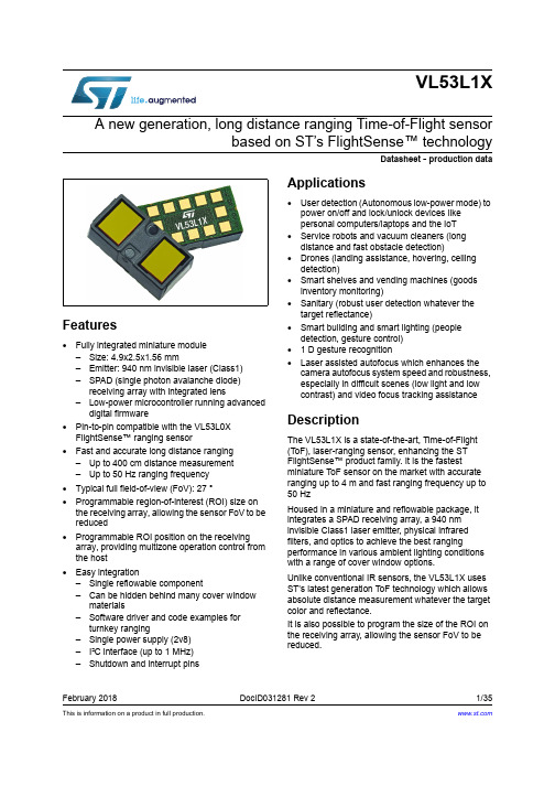
VL53L1规格书
3.2.2 Repeatability definition . . . . . . . . . . . . . . . . . . . . . . . . . . . . . . . . . . . . . . 16
• Pin-to-pin compatible with the VL53L0X FlightSense™ ranging sensor
• Fast and accurate long distance ranging – Up to 400 cm distance measurement – Up to 50 Hz ranging frequency
3.2 Accuracy, repeatability, and ranging error definitions . . . . . . . . . . . . . . . . 16
3.2.1 Accuracy definition . . . . . . . . . . . . . . . . . . . . . . . . . . . . . . . . . . . . . . . . . 16
• Typical full field-of-view (FoV): 27 °
• Programmable region-of-interest (ROI) size on the receiving array, allowing the sensor FoV to be reduced
• Programmable ROI position on the receiving array, providing multizone operation control from the host
Applications
Azbil ACTIVAL 流量计和控制值阀显示面板说明书

© 2015–2016 Azbil Corporation All Rights Reserved.Display Panelfor ACTIVAL ™ Flow Measurement and Control ValveStandalone ModelGeneralDisplay Panel Model QY5010S1000 is the data indicator for ACTIVAL Flow Measurement and Control Valve ModelFVY513X. Display Panel displays data measured by Model FVY513X (flow pressure, flow temperature, flow) and valve position.Besides, the setting buttons on the Display Panel allow you to set and change various data.Features∙Multiple data in a single displayYou can check flow temperature of AHU inlet/outlet, flow pressure of valve inlet/outlet, and flow measured by Model FVY513X and the valve position at one time. ∙Installable 164 ft (50 m) away from Model FVY513XDisplay panel is connected to Model FVY513X with AWG 22 (0.3 mm²), 4-core cable, and max. cable length is 164 ft (50 m).∙ Continuous displayDisplay Panel displays data all the time. You can thus check flow conditions and valve position at any time. ∙Compact and lightweightSmall and light body facilitates installation on an AHU panel or inside a control panel cabinet.∙ Easy wiringSince Display Panel main unit is connected to the base plate with the connector inside, wiring to Display Panel is complete only by connecting the wires to the base plate. ∙Parameter setting and error code check availableDisplay Panel allows you to set parameters and check error codes of Model FVY513X.∙CE Marking certifiedThis product conforms to all the applicable standards of CE Marking.AB-7358-USafety InstructionsPlease read instructions carefully and use the product as specified in this manual. Be sure to keep this manual nearby for quick reference.Usage RestrictionsThis product is targeted for general air conditioning. Do not use this product in a situation where human life might be affected. Also, do not install this product in an atmosphere containing explosive gas or flammable gas.If this product is used in a clean room or a place where particularly high reliability or control accuracy is required, please contact our sales representative. Azbil Corporation will not bear any responsibility for the results produced by the operators.Warnings and CautionsWARNING Alerts users that improper handling may cause death or serious injury.CAUTION Alerts users that improper handling may cause minor injury or material loss.SignsAlerts users possible hazardous conditions caused by erroneous operation or erroneous use. The symbol inside I indicates the specific type of danger.(For example, the sign on the left warns of the risk of electric shock.)Notifies users that specific actions are prohibited to prevent possible danger. The symbol inside Q graphically indicates the prohibited action.(For example, the sign on the left notifies that disassembly is prohibited.)Instructs users to carry out a specific obligatory action to prevent possible danger. The symbol inside d graphically indicates the actual action to be carried out.(For example, the sign on the left indicates general instructions.)WARNINGBefore wiring or maintenance, be sure to turn off the power to the product.Failure to do so might cause electric shock or device failure.CAUTIONInstall and use the product under the operating conditions (for temperature, humidity, power, vibration, shock, mounting direction, atmospheric condition, etc.) as listed in the specifications.Failure to do so might cause fire or device failure.Installation and wiring must be performed by qualified personnel in accordance with all applicable safety standards. All wiring must comply with applicable codes and ordinances.Take anti-lightening measures based on regional and building characteristics.Lightening might cause fire or critical damage to the products without the anti-lightening measures.If more than the rated power voltage is applied to the product, replace the product with new one for your safety.Failure to do so might cause device failure or overheating.Do not disassemble the product.Doing so might cause device failure.Dispose of the product as industrial waste in accordance with your local regulations.Do not reuse all or part of this product.AB-7358-U IMPORTANT:In case an Azbil Corporation product fails, you are required to provide your Equipment with safety design suchas fool-proof design*1, and fail-safe design*2 (anti-flame propagation design, etc.), whereby preventing anyoccurrence of physical injuries, fires, significant damage, and so forth. Furthermore, fault avoidance*3, faulttolerance*4, or the like should be incorporated so that the said Equipment can satisfy the level of reliability andsafety required for your use.*1. A design that is safe even if the user makes an error.*2. A design that is safe even if the device fails.*3. Avoidance of device failure by using highly reliable components, etc.*4. The use of redundancy.Note: This equipment has been tested and found to comply with the limits for a Class A digital device, pursuant to part 15 of the FCC Rules. These limits are designed to provide reasonable protection against harmful interference when theequipment is operated in a commercial environment. This equipment generates, uses, and can radiate radio frequencyenergy and, if not installed and used in accordance with the instruction manual, may cause harmful interference to radiocommunications. Operation of this equipment in a residential area is likely to cause harmful interference in which casethe user will be required to correct the interference at his own expense.Model NumberModel number DescriptionQY5010 Base model number of Display Panel for Model FVY513XS1000S-001 Power supplied from ACTIVAL Flow Measurement and Control Valve standalone model (Model FVY513X)SpecificationsItem Specification Power supply 12 V DC ± 1 V (supplied from Model FVY513X)Power consumption Max. 0.1 VACable AWG 22 (0.3 mm2) , 4-core cableEnvironmental conditions Rated operatingcondition*1Ambient temperature 32 ︒F to 122 ︒F (0 ︒C to 50 ︒C)Ambient humidity 10 % RH to 85 % RH (non-condensing)Vibration 19.4fps2 (5.9 m/s2), 10 Hz to 150 Hz Transport/storageconditionsAmbient temperature -4 ︒F to 158 ︒F (-20 ︒C to 70 ︒C)Ambient humidity 10 % RH to 85 % RH (non-condensing)Vibration 32.2fps2 (9.8 m/s2), 10 Hz to 150 HzEnclosure rating IEC IP40 (dustproof)Display*2Device Liquid Crystal Display (LCD)Items to display Pvin Valve inlet pressure (psig)Pvout Valve outlet pressure (psig)Q Actual flow (GPM)T1 Coil inlet temperature (︒F)T2 Coil outlet temperature (︒F)HC Heat/CoolE ErrorOpening Actual valve position (% in bar graph)Flowrate Actual flow rate (% in bar graph) Communication Transmissionsystem AP-bus (RS-485 communication)Transmission speed 4800 bpsTransmission distance Max. 164 ft (50 m)Number of Display PanelconnectableOne per single Model FVY513XMaterials Case Modified polyphenylene ether (PPE)Base plate Modified polyphenylene ether (PPE)Face plate Polyester (PET)Accessory - Two tapping screws (M4) for mounting- Two 'kPa' unit stickersWeight 0.33 lb (150 g)Notes:*1 LCD service life may shorten if Display Panel is used in an environment with high temperature and humidity. *2 For display accuracy, refer to specification data of Model FVY513X.AB-7358-URecommended Wire SpecificationsCable typeWiring lengthAWG 22 (0.3 mm 2), 4-core(Cable is not supplied with Display Panel.)164 ft (50 m)OptionItem Note Waterproof boxPart No. 83170324-001 Required when Display Panel is installed outdoors.CE Marking ConformityThis product complies with the following Electromagnetic Compatibility (EMC).EMC : EN61326-1 Class A Table 2 (For use in an industrial electromagnetic environment)DimensionsOutside dimensionsFigure 1. Outside dimensionsMounting dimensions of the base plateFigure 2. Mounting dimensions of the base plate1.89" (48 mm) 1.89" (48 mm)1.30" (33 mm)0.59" (15 m m )2.60" (66 m m )Mounting holesCable conduitHook to remove the casefrom the base plate0.59" (15 m m )2.03" (51.5 m m )3.78" (96 mm)3.78" (96 m m )Base plate CaseAB-7358-U Parts IdentificationFigure 3. Parts identification from the base plate Face plateInsertion guide (female)LCD Insertion guide (male)AB-7358-UItems to be displayed on LCDAnalog values such as pressure, flow, and temperature are displayed on the LCD. Setting buttons set/change various parameters and display error description (when an error occurs). Be sure to enable the parameter setting (Parameter 60) before changing any parameters. For details, see AB-7363-U Instruction Manual of ACTIVAL Flow Measurement and Control Valve Standalone Model .Analog values display screenAnalog values display screen appears on the LCD when you turn on the Display Panel.Figure 4. Analog values display screenDisplay areaDescriptionDisplay rangeUnit Item Display Panel connected to: Range 1 Pvin Valve inlet pressure Model FVY5137 0 to 160 psig Model FVY513E 0 to 320 psig 2PvoutValve outlet pressureModel FVY5137 0 to 160 psig Model FVY513E0 to 320psig 3 QActual flow0.000 to 999.9 GPM 4 T 1Coil inlet temperature 14 to 212 °F 5 T 2Coil outlet temperature14 to 212°F Opening Valve position indicated in a bar graph 0 to 100 (with every 10 % increment) % Flowrate Flow indicated in a bar graph 0 to 100 (with every 10 % increment) % E Error occurred ([E] flashes.)− − H C AHU operation mode ([H]: Heat / [C]: Cool)−−Setting buttonsFunction[→] Cursor button Not used in the analog values display screen.[∨] Down button Press this button to switch to the error display screen when the error indicator [E] flashes. [∧] Up buttonPress this button to switch to the error display screen when the error indicator [E] flashes. [ENT] Enter buttonPress and hold this button to switch to the parameter setting screen.Heat/Cool operation modeindicatorDisplay area 1Enter buttonError indicatorDisplay area 2Display area 3 Display area 4Display area 5Up button Down button Cursor button Valve position in bar graphFlow rate in bar graphAB-7358-U● Parameter setting screenPress and hold the [ENT] button to switch to the parameter setting screen from the analog values display screen.Figure 5. Parameter setting screenDisplay area Display item1indicating the parameter setting screen2 Parameter number3 Current setpoint set for the parameter shown in thedisplay area 2.4 No item displayed5 No item displayedSetting buttons Function [→] Cursor button Press this button to select the digit of theparameter number and of the setpoint. The selected digit flashes.[∨] Down button Press this button to change the selected digit.[∧] Up button Press this button to change the selected digit.[ENT] Enter button Press this button to finally set the changedparameter.Press and hold this button to go back to the analog values display screen.Note:No button operation for continuous 10 minutes on the parameter setting screen will automatically switch from the parameter setting screen to the analog values display screen.● Error display screenFigure 6. Error display screenDisplay area Display item [E] Error occurred 1indicating the error display screen2 Error code3 No item displayed4 No item displayed5 No item displayedSetting buttons Function [→] Cursor button Not used in the error display screen. [∨] Down button Press this button to go back to the analogvalues display screen.[∧] Up button Press this button to go back to the analogvalues display screen.[ENT] Enter button Not used in the error display screen. Note:For details of the error codes, refer to AB-7363-U Instruction Manual of ACTIVAL Flow Measurement and Control Valve Standalone Model .Display area 1Display area 2Display area 1Display area 2Display area 3AB-7358-UWiring and InstallationWARNINGBefore wiring or maintenance, be sure to turn off the power to the product.Failure to do so might cause electric shock or device failure.Wiring1) Press the hook on the bottom of the base plate and detach the case.2) Use 0.22" Dia. to 0.24" Dia. (5.5 mm Dia. to 6.0 mm Dia) cable (AWG 22 (0.3 mm2) , 4-core cable recommended) forconnection. Strip 0.20" to 0.24"(5 mm to 6 mm) sheath of each lead wire. (See Fig. 7.)3) Refer to the wiring label (attached to the base plate) and insert stripped lead wires to each terminal.TerminalsarrangementTerminal number Type Lead wire color*1 12 V DC (+) Red (RED)2 0 V Black (BLK)3 AP-bus (+) White (WHT)4 AP-bus (-) Green (GRN)Note: Lead wire color shown in the above table is the wirecolors of the recommended cable.4) Lock each lead wire with lever lock provided on each terminal. Use a tool such as slotted screwdriver to slide the lever lock.Figure 8. Lead wire connection5) Insert the cable into the slit and fix the cable on the base plate with a cable tie.Figure 9. Cable fixed on the base plate0.20" to 0.24"CableAB-7358-UInstallationIMPORTANT:∙ Do not install this product in an atmosphere containing corrosive gas or explosive gas.∙ Do not install this product in a location exposed to direct sunlight. Direct sunlight accelerates LCD degradation.∙ Waterproof box (optional) is required for the product to be installed outdoors. Ask our sales personnel for the waterproof box.Procedure1) Make two holes for two M4 tapping screws (one for upper and the other for lower sides) on a mounting location, such as anAHU side plate or a panel cabinet. Distance between the centers of upper and lower M4 screws is 2.6" ± 0.08" (66 ± 2 mm). 2) Lead the cable (connected to the base plate terminals) out of the base plate through the base plate conduit (on the bottomright), and mount the base plate on the mounting location with the two M4 tapping screws (accessory of Display Panel).Figure 10. Mounting of the base plate with two M4 tapping screws3) Assemble the case with the base plate by inserting the male insertion guide of the case into the female insertion guide of thebase plate. Four insertion guides are provided on the right and left sides (Two on each side). Press the case well so that the case is completely assembled with the base plate. The case is connected to the base plate with the internal connector.Figure 11. Case assembly with the base plateTwo M4 tapping screwsCable conduit(female)Insertion guides (male)CaseAB-7358-U4) Arrange the cable connected to Display Panel.Cautions for arranging the cable: ∙ Do not pull the cable. ∙ To prevent water from flowing down to Display Panel through the cable, let the cable sag, as Fig. 12 shows. ∙ When installing Display Panel on an AHU side plate, seal the wiring hole on the AHU side plate, as Fig. 12 shows. Damp or dew condensation may damage the Display Panel, otherwise.Figure 12. Cable arrangement5) Film is attached to the front surface (face plate) of Display Panel for protection before shipment. Remove the film beforeactivating Display Panel.6) Display Panel is generally installed on a visible position such as on a wall in a machine room or on a control panel cabinet.However, it may possibly be installed outdoors or in a ceiling. In such a case, install the Display Panel as shown in Figs. 13 and 14. Consider the conditions and requirements of your Display Panel installation and decide the location.Figure 13. Display Panel installed outdoors (in a rainproof box)Display PanelSealing materialCableLet the cable sag.Cable led out of the rear side of Display PanelCable led through the conduit of Display Panel 2" (50 mm) stanchionDisplay Panel in a protection boxDisplay Panel in a protection box directly on a wall2" (50 mm) stanchion Display Panel in a plastic box(commercially available)AB-7358-U If Display Panel needs to be installed in a ceiling, install it near the ceiling access panel. Mount Display Panel in a dustproof box to install in a dusty area in a ceiling.Details of AFigure 14. Display Panel installed in a ceilingWiring to Model FVY513XIMPORTANT:Do not pull the cable connected from the terminals of Display Panel to the terminals of Model FVY513X. Display Panel is used in combination with Model FVY513X. To connect the cable to Model FVY513X, refer to Specification/Installation of Model FVY513X.- AB-7350-U: ACTIVAL Flow Measurement and Control Valve Standalone Model Models FVY5137J (PN10/GG-20)- AB-7354-U: ACTIVAL Flow Measurement and Control Valve Standalone Model Models FVY513EJ (JIS 20K/SCPH2)MaintenanceFor replacement of Display Panel, whole unit must be replaced. Display Panel cannot be partially replaced.Care for the face plateClean the face plate with dry soft cloth. Never use detergent or organic solvent to clean the screen. Otherwise, LCD screen will get scratched, discolored, or deformed.AB-7358-URev. 3.0 Jun. 2016 AB-7358-U。
AVS1ACP08中文资料
4/8
元器件交易网
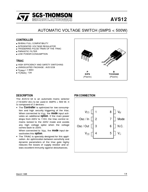
AVS12
DC GENERAL ELECTRICAL CHARACTERISTICS (continued) CONTROLLER AVS1ACP08 Toper = 25°C (unless otherwise specified)
Symbo l
P ar ame te r
0.7 Vreg
0.3 Vreg
V
VG (pin 5)
VOL (IVG = 25mA) Leakage current (VG = VDD)
650
mV
+ 10
µA
NOTES : (1) : This value gives a typical noise immunity on the zero-crossing detection of 110mV x 1018/18 = 6.20V on the main supply (2) : See following diagram (3) : Voltage referred to VSS (4) : Voltage referred to VDD
5/8
元器件交易网
AVS12
TYPICAL APPLICATION
110 V or 220V
1N 4007
R1 1M 1%
2
x
R2
9.1K
18K
1W
1%
option VDD AVS12CB
VM 8
7 AVS1ACP08
VSS 390
5 VG
A2 G A1
3 2
91k 1 %
Symb ol
P a ra met er
VGD VTM *
NU513线性 恒流芯片规格书

TOEFall
OE timing diagram
Test Cirቤተ መጻሕፍቲ ባይዱuit
Output Current Setting
The output current of NU513 is set by an external resistor (REXT). The output current can be figured out by following equation.
Load OPT
Vrefence OE GND
Rext
-1Please visit for more patent information.
Ver.01 -3-658-9936 FAX: +886-3-550-2805
3F., No. 96, Sec. 1, Jiafong 6th Road, Jhubei City, Hsinchu County 302, Taiwan. TEL: +886
IOPT PDRMP
PD ≤ PDRMP (Ta=25°C)
1.5V ≤ VDD ≤ 16V
mA W
ILeakage %/VDD %/VP %/10℃ VIH
VOPT = 10V
OE = 0V VDD ≤ 0.2V
3.2
0.7*VDD
160 115 3
0.5 ±1 ±1 ±0.5 2
0.3*VDD
uA %/V %/V
Iout
0.195V REXT 0.2
-4Please visit for more patent information.
Ver.01 TEL: +886-3-658-9936 FAX: +886-3-550-2805