HD74LS139RPEL中文资料
74193中文资料
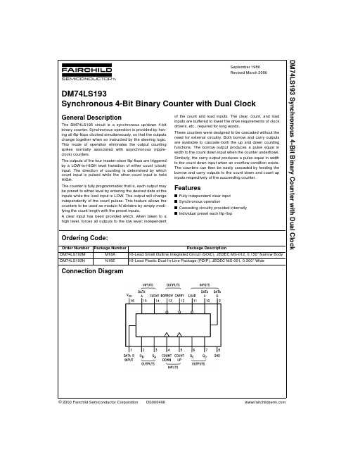
© 2000 Fairchild Semiconductor Corporation DS006406September 1986Revised March 2000DM74LS193 Synchronous 4-Bit Binary Counter with Dual ClockDM74LS193Synchronous 4-Bit Binary Counter with Dual ClockGeneral DescriptionThe DM74LS193 circuit is a synchronous up/down 4-bit binary counter. Synchronous operation is provided by hav-ing all flip-flops clocked simultaneously, so that the outputs change together when so instructed by the steering logic.This mode of operation eliminates the output counting spikes normally associated with asynchronous (ripple-clock) counters.The outputs of the four master-slave flip-flops are triggered by a LOW-to-HIGH level transition of either count (clock)input. The direction of counting is determined by which count input is pulsed while the other count input is held HIGH.The counter is fully programmable; that is, each output may be preset to either level by entering the desired data at the inputs while the load input is LOW. The output will change independently of the count pulses. This feature allows the counters to be used as modulo-N dividers by simply modi-fying the count length with the preset inputs.A clear input has been provided which, when taken to a high level, forces all outputs to the low level; independent of the count and load inputs. The clear, count, and load inputs are buffered to lower the drive requirements of clock drivers, etc., required for long words.These counters were designed to be cascaded without the need for external circuitry. Both borrow and carry outputs are available to cascade both the up and down counting functions. The borrow output produces a pulse equal in width to the count down input when the counter underflows.Similarly, the carry output produces a pulse equal in width to the count down input when an overflow condition exists.The counters can then be easily cascaded by feeding the borrow and carry outputs to the count down and count up inputs respectively of the succeeding counter.Featuress Fully independent clear input s Synchronous operations Cascading circuitry provided internally s Individual preset each flip-flopOrdering Code:Connection DiagramOrder Number Package NumberPackage DescriptionDM74LS193M M16A 16-Lead Small Outline Integrated Circuit (SOIC), JEDEC MS-012, 0.150” Narrow Body DM74LS193NN16E16-Lead Plastic Dual-In-Line Package (PDIP), JEDEC MS-001, 0.300” Wide 2D M 74L S 193Logic Diagram DM74LS193Timing DiagramNote A: Clear overrides load, data, and count inputsNote B: When counting up, count-down input must be HIGH; when counting down, count-up input must be HIGH. 4D M 74L S 193Absolute Maximum Ratings (Note 1)Note 1: The “Absolute Maximum Ratings” are those values beyond which the safety of the device cannot be guaranteed. The device should not be operated at these limits. The parametric values defined in the Electrical Characteristics tables are not guaranteed at the absolute maximum ratings.The “Recommended Operating Conditions” table will define the conditions for actual device operation.Recommended Operating ConditionsNote 2: C L = 15 pF, R L = 2 k Ω, I A = 25°C and V CC = 5V.Note 3: C L = 50 pF, R L = 2 k Ω, I A = 25°C and V CC = 5V.Note 4: T A = 25°C and V CC = 5V.DC Electrical CharacteristicsNote 5: All typicals are at V CC = 5V, T A = 25°C.Note 6: Not more than one output should be shorted at a time, and the duration should not exceed one second.Note 7: I CC is measured with all outputs open, CLEAR and LOAD inputs grounded, and all other inputs at 4.5V.Operating Free Air Temperature Range −0°C to +70°CSupply Voltage 7V Input Voltage7VStorage Temperature Range−65°C to +125°CSymbol ParameterMin Nom Max Units V CC Supply Voltage4.7555.25V V IH HIGH Level Input Voltage 2V V IL LOW Level Input Voltage 0.8V I OH HIGH Level Output Current −0.4mA I OL LOW Level Output Current 8mA f CLK Clock Frequency (Note 2)025MHz Clock Frequency (Note 3)t W Pulse Width of any Input (Note 4)20ns t SU Data Setup Time (Note 4)20ns t H Data Hold Time (Note 4)0ns t EN Enable Time to Clock (Note 4)40ns T AFree Air Operating Temperature70°CSymbol ParameterConditionsMin Typ Max Units (Note 5)V I Input Clamp Voltage V CC = Min, I I = −18 mA −1.5V V OH HIGH Level Output V CC =Min,I OH =Max 2.5 3.4VVoltageV IL = Max, V IH = Min 2.73.4V OLLOW Level Output V CC =Min,I OL =Max 0.250.4VoltageV IL = Max, V IH = Min 0.350.5V I OL =4mA,V CC =Min 0.250.4I I Input Current @ Max Input Voltage V CC = Max, V I = 7V 0.1mA I IH HIGH Level Input Current V CC = Max, V I = 2.7V 20µA I IL LOW Level Input Current V CC = Max, V I = 0.4V −0.4mA I OS Short Circuit V CC = Max −20−100mA Output Current (Note 6)−20−100I CCSupply CurrentV CC = Max (Note 7)1934mADM74LS193 AC Electrical CharacteristicsFrom (Input)R L= 2 kΩSymbol Parameter To (Output)C L= 15 pF C L= 50 pF UnitsMin Max Min Maxf MAX Maximum Clock Frequency2520MHzt PLH Propagation Delay Time Count Up2630ns LOW-to-HIGH Level Output to Carryt PHL Propagation Delay Time Count Up2436ns HIGH-to-LOW Level Output to Carryt PLH Propagation Delay Time Count Down2429ns LOW-to-HIGH Level Output to Borrowt PHL Propagation Delay Time Count Down2432ns HIGH-to-LOW Level Output to Borrowt PLH Propagation Delay Time Either Count3845ns LOW-to-HIGH Level Output to Any Qt PHL Propagation Delay Time Either Count4754ns HIGH-to-LOW Level Output to Any Qt PLH Propagation Delay Time Load to4041ns LOW-to-HIGH Level Output Any Qt PHL Propagation Delay Time Load to4047ns HIGH-to-LOW Level Output Any Qt PHL Propagation Delay Time Clear to3544ns HIGH-to-LOW Level Output Any Q 6D M 74L S 193Physical Dimensionsinches (millimeters) unless otherwise noted16-Lead Small Outline Integrated Circuit (SOIC), JEDEC MS-012, 0150” Narrow BodyPackage Number M16APhysical Dimensions inches (millimeters) unless otherwise noted (Continued)16-Lead Plastic Dual-In-Line Package (PDIP), JEDEC MS-001, 0.300” WidePackage Number N16EFairchild does not assume any responsibility for use of any circuitry described, no circuit patent licenses are implied and Fairchild reserves the right at any time without notice to change said circuitry and specifications.LIFE SUPPORT POLICYFAIRCHILD’S PRODUCTS ARE NOT AUTHORIZED FOR USE AS CRITICAL COMPONENTS IN LIFE SUPPORT DEVICES OR SYSTEMS WITHOUT THE EXPRESS WRITTEN APPROVAL OF THE PRESIDENT OF FAIRCHILD SEMICONDUCTOR CORPORATION. As used herein:1.Life support devices or systems are devices or systemswhich, (a) are intended for surgical implant into the body, or (b) support or sustain life, and (c) whose failure to perform when properly used in accordance with instructions for use provided in the labeling, can be rea-sonably expected to result in a significant injury to the user.2. A critical component in any component of a life supportdevice or system whose failure to perform can be rea-sonably expected to cause the failure of the life support device or system, or to affect its safety or effectiveness. DM74LS193 Synchronous 4-Bit Binary Counter with Dual Clock。
74ls192

74ls192/74ls193中文资料介绍时间:2009-06-21 07:37:29 来源:资料室作者:74LS192同步可逆递增/递减BCD 计数器74LS193同步可逆递增/递减四位二进制计数器特点:电路可进行反馈,而很容易的被级联。
即把借位输出端和进位输出端分别反馈到后级计数器的减计数输入端和加计数输入端上即可。
·芯片内部有级联电路·同步操作·每触发器有单独的预置端·完全独立的清零输入端真值表:H=高电平L=低电平X=不定(高或低电平)↑=由―低‖→―高‖电平的跃变引脚功能表:图1 74LS192 逻辑图图2 74LS193 逻辑图图3 74LS192/74LS193引脚图图4 逻辑符号图5 74LS192 状态图图6 74LS192 状态图Operating Conditions 建议操作条件:DC SPECIFICATIONS直流电气规格:交流安装要求(TA =25℃)图7 交流波形应用电路图:图8图9原理:本电路复杂程度为55个等效门。
本电路通过同时触发所有触发器而提供同步操作,以便在使用控制逻辑结构时,输出端的变化可相互重合。
本工作方式避免了一般用异步(行波时钟)计数器所带来的计数输出的尖峰脉冲。
四个主从触发器的输出端,由两计数(时钟)输入之一的―低‖到―高‖电平的过渡而被触发。
计数方向在其它计数输入端为―高‖时,由脉冲的计数输入端所定。
本电路为全可编程的,当置数输入为―低‖时,把所希望的数据送入数据输入端上,来把每个输出端预置到两电平之一。
输出将符合独立于计数脉冲的数据输入的改变。
该特点可使电路以预置输入而简单地更改计数长度,用作N 模数分频器(除法器)。
清零输入在加高电平时,迫使所有输出端为低电平。
清零功能独立于计数输入和置数输入。
清零、计数和置数等输入端都是缓冲过的,它降低了驱动的要求,这就可减少为长字所要求的时钟驱动器数等等。
本电路都设计成可被直接级联而勿需外接电路。
译码器74LS139

TL F 639154LS138 DM54LS138 DM74LS138 54LS139 DM54LS139 DM74LS139Decoders DemultiplexersJune 198954LS138 DM54LS138 DM74LS138 54LS139 DM54LS139 DM74LS139Decoders DemultiplexersGeneral DescriptionThese Schottky-clamped circuits are designed to be used in high-performance memory-decoding or data-routing appli-cations requiring very short propagation delay times In high-performance memory systems these decoders can be used to minimize the effects of system decoding When used with high-speed memories the delay times of these decoders are usually less than the typical access time of the memory This means that the effective system delay intro-duced by the decoder is negligibleThe LS138decodes one-of-eight lines based upon the con-ditions at the three binary select inputs and the three enable inputs Two active-low and one active-high enable inputs reduce the need for external gates or inverters when ex-panding A 24-line decoder can be implemented with no ex-ternal inverters and a 32-line decoder requires only one inverter An enable input can be used as a data input for demultiplexing applicationsThe LS139comprises two separate two-line-to-four-line de-coders in a single package The active-low enable input can be used as a data line in demultiplexing applications All of these decoders demultiplexers feature fully buffered inputs presenting only one normalized load to its driving circuit All inputs are clamped with high-performanceSchottky diodes to suppress line-ringing and simplify system designFeaturesYDesigned specifically for high speed Memory decodersData transmission systemsYLS1383-to-8-line decoders incorporates 3enable in-puts to simplify cascading and or data receptionYLS139contains two fully independent 2-to-4-line decod-ers demultiplexersY Schottky clamped for high performance YTypical propagation delay (3levels of logic)LS13821ns LS13921nsYTypical power dissipation LS13832mW LS13934mW YAlternate Military Aerospace devices (54LS138 54LS139)are available Contact a National Semicon-ductor Sales Office Distributor for specificationsConnection DiagramsDual-in-Line PackageTL F 6391–1Order Number 54LS138DMQB 54LS138FMQB 54LS138LMQB DM54LS138J DM54LS138WDM74LS138M or DM74LS138N See NS Package Number E20A J16AM16A N16E or W16ADual-in-Line PackageTL F 6391–2Order Number 54LS139DMQB 54LS139FMQB 54LS139LMQB DM54LS139J DM54LS139WDM74LS139M or DM74LS139N See NS Package Number E20A J16AM16A N16E or W16AC 1995National Semiconductor CorporationRRD-B30M105 Printed in U S AAbsolute Maximum Ratings(Note)If Military Aerospace specified devices are required please contact the National Semiconductor Sales Office Distributors for availability and specifications Supply Voltage7V Input Voltage7V Operating Free Air Temperature RangeDM54LS and54LS b55 C to a125 C DM74LS0 C to a70 C Storage Temperature Range b65 C to a150 C Note The‘‘Absolute Maximum Ratings’’are those values beyond which the safety of the device cannot be guaran-teed The device should not be operated at these limits The parametric values defined in the‘‘Electrical Characteristics’’table are not guaranteed at the absolute maximum ratings The‘‘Recommended Operating Conditions’’table will define the conditions for actual device operationRecommended Operating ConditionsSymbol ParameterDM54LS138DM74LS138Units Min Nom Max Min Nom MaxV CC Supply Voltage4 555 54 7555 25V V IH High Level Input Voltage22V V IL Low Level Input Voltage0 70 8V I OH High Level Output Current b0 4b0 4mA I OL Low Level Output Current48mA T A Free Air Operating Temperature b55125070 C’LS138Electrical Characteristicsover recommended operating free air temperature range(unless otherwise noted)Symbol Parameter Conditions MinTypMax Units (Note1)V I Input Clamp Voltage V CC e Min I I e b18mA b1 5V V OH High Level Output V CC e Min I OH e Max DM542 53 4V Voltage V IL e Max V IH e Min DM742 73 4V OL Low Level Output V CC e Min I OL e Max DM540 250 4 Voltage V IL e Max V IH e Min DM740 350 5VI OL e4mA V CC e Min DM740 250 4I I Input Current Max V CC e Max V I e7V0 1mAInput VoltageI IH High Level Input Current V CC e Max V I e2 7V20m A I IL Low Level Input Current V CC e Max V I e0 4V b0 36mAI OS Short Circuit V CC e Max DM54b20b100mA Output Current(Note2)DM74b20b100I CC Supply Current V CC e Max(Note3)6 310mA Note1 All typicals are at V CC e5V T A e25 CNote2 Not more than one output should be shorted at a time and the duration should not exceed one secondNote3 I CC is measured with all outputs enabled and open2’LS138Switching Characteristicsat V CC e5V and T A e25 C(See Section1for Test Waveforms and Output Load)From(Input)LevelsR L e2k XSymbol Parameter To(Output)of Delay C L e15pF C L e50pF UnitsMin Max Min Maxt PLH Propagation Delay Time Select to21827ns Low to High Level Output Outputt PHL Propagation Delay Time Select to22740ns High to Low Level Output Outputt PLH Propagation Delay Time Select to31827ns Low to High Level Output Outputt PHL Propagation Delay Time Select to32740ns High to Low Level Output Outputt PLH Propagation Delay Time Enable to21827ns Low to High Level Output Outputt PHL Propagation Delay Time Enable to22440ns High to Low Level Output Outputt PLH Propagation Delay Time Enable to31827ns Low to High Level Output Outputt PHL Propagation Delay Time Enable to32840ns High to Low Level Output OutputRecommended Operating ConditionsSymbol ParameterDM54LS139DM74LS139Units Min Nom Max Min Nom MaxV CC Supply Voltage4 555 54 7555 25V V IH High Level Input Voltage22V V IL Low Level Input Voltage0 70 8V I OH High Level Output Current b0 4b0 4mA I OL Low Level Output Current48mA T A Free Air Operating Temperature b55125070 C3’LS139Electrical Characteristicsover recommended operating free air temperature range(unless otherwise noted)Symbol Parameter Conditions MinTypMax Units (Note1)V I Input Clamp Voltage V CC e Min I I e b18mA b1 5V V OH High Level Output V CC e Min I OH e Max DM542 53 4V Voltage V IL e Max V IH e Min DM742 73 4V OL Low Level Output V CC e Min I OL e Max DM540 250 4 Voltage V IL e Max V IH e Min DM740 350 5VI OL e4mA V CC e Min DM740 250 4I I Input Current Max V CC e Max V I e7V0 1mAInput VoltageI IH High Level Input Current V CC e Max V I e2 7V20m A I IL Low Level Input Current V CC e Max V I e0 4V b0 36mAI OS Short Circuit V CC e Max DM54b20b100mA Output Current(Note2)DM74b20b100I CC Supply Current V CC e Max(Note3)6 811mA Note1 All typicals are at V CC e5V T A e25 CNote2 Not more than one output should be shorted at a time and the duration should not exceed one secondNote3 I CC is measured with all outputs enabled and open’LS139Switching Characteristicsat V CC e5V and T A e25 C(See Section1for Test Waveforms and Output Load)From(Input)R L e2k XSymbol Parameter To(Output)C L e15pF C L e50pF UnitsMin Max Min Maxt PLH Propagation Delay Time Select to1827ns Low to High Level Output Outputt PHL Propagation Delay Time Select to2740ns High to Low Level Output Outputt PLH Propagation Delay Time Enable to1827ns Low to High Level Output Outputt PHL Propagation Delay Time Enable to2440ns High to Low Level Output OutputFunction TablesLS138InputsOutputsEnable SelectG1G2 C B A YO Y1Y2Y3Y4Y5Y6Y7 X H X X X H H H H H H H H L X X X X H H H H H H H H H L L L L L H H H H H H H H L L L H H L H H H H H H H L L H L H H L H H H H H H L L H H H H H L H H H H H L H L L H H H H L H H H H L H L H H H H H H L H H H L H H L H H H H H H L H H L H H H H H H H H H H L G2e G2A a G2BH e High Level L e Low Level X e Don’t CareLS139InputsOutputsEnable SelectG B A Y0Y1Y2Y3H X X H H H HL L L L H H HL L H H L H HL H L H H L HL H H H H H LH e High Level L e Low Level X e Don’t Care4Logic DiagramsLS138TL F 6391–3LS139TL F 6391–45Physical Dimensions inches(millimeters)Ceramic Leadless Chip Carrier Package(E)Order Number54LS138LMQB or54LS139LMQBNS Package Number E20A16-Lead Ceramic Dual-In-Line Package(J)Order Number54LS138DMQB 54LS139DMQB DM54LS138J or DM54LS139JNS Package Number J16A6Physical Dimensions inches(millimeters)(Continued)16-Lead Small Outline Molded Package(M)Order Number DM74LS138M or DM74LS139MNS Packge Number M16A16-Lead Molded Dual-In-Line Package(N)Order Number DM74LS138N or DM74LS139NNS Package Number N16E754L S 138 D M 54L S 138 D M 74L S 138 54L S 139 D M 54L S 139 D M 74L S 139D e c o d e r s D e m u l t i p l e x e r sPhysical Dimensions inches (millimeters)(Continued)16-Lead Ceramic Flat Package (W)Order Number 54LS138FMQB 54LS139FMQB DM54LS138W or DM54LS139WNS Package Number W16ALIFE SUPPORT POLICYNATIONAL’S PRODUCTS ARE NOT AUTHORIZED FOR USE AS CRITICAL COMPONENTS IN LIFE SUPPORT DEVICES OR SYSTEMS WITHOUT THE EXPRESS WRITTEN APPROVAL OF THE PRESIDENT OF NATIONAL SEMICONDUCTOR CORPORATION As used herein 1 Life support devices or systems are devices or 2 A critical component is any component of a life systems which (a)are intended for surgical implant support device or system whose failure to perform can into the body or (b)support or sustain life and whose be reasonably expected to cause the failure of the life failure to perform when properly used in accordance support device or system or to affect its safety or with instructions for use provided in the labeling can effectivenessbe reasonably expected to result in a significant injury to the userNational Semiconductor National Semiconductor National Semiconductor National Semiconductor CorporationEuropeHong Kong LtdJapan Ltd1111West Bardin RoadFax (a 49)0-180-530858613th Floor Straight Block Tel 81-043-299-2309。
74hc139中文资料参数
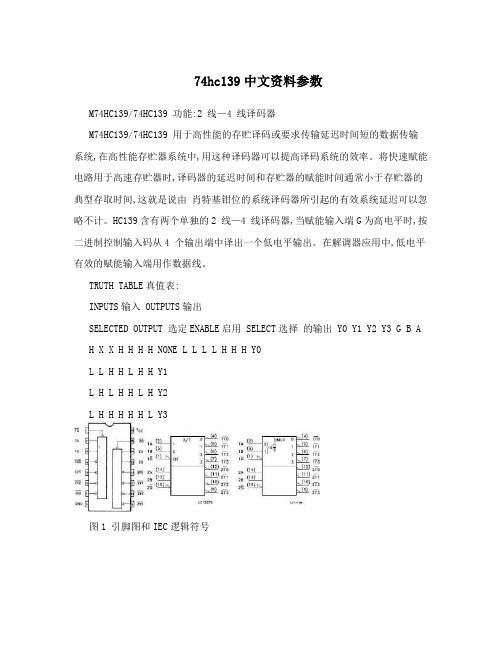
74hc139中文资料参数M74HC139/74HC139 功能:2 线—4 线译码器M74HC139/74HC139 用于高性能的存贮译码或要求传输延迟时间短的数据传输系统,在高性能存贮器系统中,用这种译码器可以提高译码系统的效率。
将快速赋能电路用于高速存贮器时,译码器的延迟时间和存贮器的赋能时间通常小于存贮器的典型存取时间,这就是说由肖特基钳位的系统译码器所引起的有效系统延迟可以忽略不计。
HC139含有两个单独的2 线—4 线译码器,当赋能输入端G为高电平时,按二进制控制输入码从4 个输出端中译出一个低电平输出。
在解调器应用中,低电平有效的赋能输入端用作数据线。
TRUTH TABLE真值表:INPUTS输入 OUTPUTS输出SELECTED OUTPUT 选定ENABLE启用 SELECT选择的输出 Y0 Y1 Y2 Y3 G B AH X X H H H H NONE L L L L H H H Y0L L H H L H H Y1L H L H H L H Y2L H H H H H L Y3图1 引脚图和IEC逻辑符号图2 输入输出等效电路图3 逻辑图引脚功能表:引脚位 SYMBOL 符号 NAME AND FUNCTION名称及功能1,15 1G,2G Enable Inputs使能输入2,3 1A,1B Address Inputs地址输入4,5,6,7 1Y0 to 1Y3 Outputs输出12,11,10,9 2Y0 to 2Y3 Outputs输出14,13 2A,2B Address Inputs地址输入8 GND Ground接地(0V)16 VCC Positive Supply Voltage正电源电压ABSOLUTE MAXIMUM RATINGS绝对最大额定值:Unit SYMBOL 符号 Parameter 参数 Value 数值单位 VCC Supply Voltage电源电压 -0.5 to +7 V VI DC Input Voltage 直流输入电压 -0.5 to VCC + 0.5 V VO DC Output Voltage直流输出电压 -0.5 to VCC + 0.5 V IIK DC Input Diode Current直流输入二极管电流 ? 20 mA IOK DC Output Diode Current直流输出二极管电流 ? 20 mA IO DC Output Current直流输出电流 ? 25 mA ICC or IGND DC VCC or Ground Current ? 50 mA PD Power Dissipation功耗 500(*) mW Tstg Storage Temperature贮藏温度 -65 to +150 ? TL Lead Temperature焊接温度 (10 sec) 300 ? RECOMMENDED OPERATING CONDITIONS建议操作条件SYMBOL Unit Parameter 参数 Value 数值符号单位 VCC Supply Voltage电源电压 2 to 6 V VI Input Voltage 输入电压 0 to VCC V VO Output Voltage 输出电压 0 to VCC V Top Operating Temperature: 操作温度:M54HC系列M74HC 系列 -55to+125 -40to +85 ?VCC = 2V 0 to 1000 tr,tf Input Rise and Fall Time输入上升和下降时间VCC = 4.5V 0 to 500 nsVCC = 6V 0 to 400 DC SPECIFICATIONS直流电气规格:Test Condition测Value 数值试条件SYMBOL Unit Parameter 参数 TA =25? 54HC and -40 to 85? -55 to 125?符号 VCC 单位 74HC 74HC 54HC(V) 最小典型最大最小最大最小最大2.0 1.5 1.5 1.5 - - - - High LevelVIH InputVoltage输入4.5 3.15 3.15 3.15 V - - - -高电平电压 6.0 4.2 4.2 4.2 - - - -2.0 0.5 0.5 0.5 - - - Low LevelVIL InputVoltage输入4.5 1.35 1.35 1.35 V - - - -低电平电压 6.0 1.8 1.8 1.8 - - - -2.0 1.9 2.0 1.9 1.9 - - -4.5 4.4 4.5 4.4 4.4 - - - High LevelVOH OutputVoltage出6.0 5.9 6.0 5.9 5.9 V - - -高电平电压 4.5 4.18 4.31 4.13 4.10 - - -6.0 5.68 5.8 5.63 5.60 - - -2.0 0.0 0.1 0.1 0.1 - - -4.5 0.0 0.1 0.1 0.1 - - - Low LevelVOL OutputVoltage输6.0 0.0 0.1 0.1 0.1 V - - -出低电平电压 4.5 0.17 0.26 0.33 0.40 - - -6.0 0.18 0.26 0.33 0.40 - - -Input LeakageII Current输入漏电6.0 VI=VCC or GND ?0.1 ?1 ?1 μA - - - -流Quiescent SupplyICC Current静态电源6.0 VI=VCC or GND 4 40 80 μA - - - -电流AC ELECTRICAL CHARACTERISTICS交流电气特性:TestConditionValue 数值测试条件 SYMBOL Unit Parameter 参数 -55 to 125? 符号单位 VCC TA =25? 54HC and 74HC - 40 to 85? 74HC 54HC(V) 最小典型最大最小最大最小最大2.0 30 75 95 110 - - - tTLH Output Transition 4.5 8 15 19 22 ns - -- tTHLTime输出过渡时间6.0 7 13 16 19 - - -2.0 45 130 165 195 - - - Propagation Delay tPLH Time 传递延迟时间4.5 15 26 33 39 ns - - - tPHL (A,B -Y) 6.0 13 22 28 33 - - -2.0 39 110 140 165 - - - Propagation Delay tPLH Time 传递延迟时间4.5 13 22 28 33 ns - - - tPHL (G -Y) 6.0 11 19 24 28 - - -Input CapacitanceCIN 5 10 10 10 pF - - - - 输入电容Power DissipationCPD (*) Capacitance功耗电46 pF - - - - - -容应用电路:图4图5 晶体管H桥电机驱动电路。
74ls139

SN74LS139Dual 1-of-4 Decoder/ DemultiplexerThe LSTTL/MSI SN74LS139 is a high speed Dual 1-of-4 Decoder/Demultiplexer. The device has two independent decoders, each accepting two inputs and providing four mutually exclusive active LOW Outputs. Each decoder has an active LOW Enable inputwhich can be used as a data input for a 4-output demultiplexer. Each half of the LS139 can be used as a function generator providing all four minterms of two variables. The LS139 is fabricated with the Schottky barrier diode process for high speed and is completely compatible with all ON Semiconductor TTL families.•Schottky Process for High Speed•Multifunction Capability•Two Completely Independent 1-of-4 Decoders•Active Low Mutually Exclusive Outputs•Input Clamp Diodes Limit High Speed Termination Effects •ESD > 3500 V oltsGUARANTEED OPERATING RANGESDevice Package ShippingORDERING INFORMATIONSN74LS139N16 Pin DIP2000 Units/Box SN74LS139D SOIC–1638 Units/Rail SN74LS139DR2SOIC–162500/T ape & Reel SN74LS139M SOEIAJ–16See Note 1 SN74LS139MEL SOEIAJ–161.For ordering information on the EIAJ version ofthe SOIC package, please contact your localON Semiconductor representative.See Note 1CONNECTION DIAGRAM DIP (TOP VIEW)Address InputsEnable (Active LOW) Input Active LOW OutputsA 0, A 1EO 0 - O 30.5 U.L.0.5 U.L.10 U.L.0.25 U.L.0.25 U.L.5 U.L.NOTES:ąa) 1 TTL Unit Load (U.L.) = 40 m A HIGH/1.6 mA LOW.HIGH LOW (Note a)LOADING PIN NAMES NOTE:The Flatpak version has the same pinouts (Connection Diagram) as the Dual InĆLine Package.a0a1a0a1aV CC = PIN 16GND = PIN 8123151413456712111092a3a LOGIC SYMBOLLOGIC DIAGRAM= PIN 16A A E A 3a 0b 1b 2b 3b1a 2a E A0a FUNCTIONAL DESCRIPTIONThe LS139 is a high speed dual 1-of-4 decoder/demultiplexer fabricated with the Schottky barrier diode process. The device has two independent decoders, each of which accept two binary weighted inputs (A 0, A 1) and provide four mutually exclusive active LOW outputs (O 0–O 3). Each decoder has an active LOW Enable (E).When E is HIGH all outputs are forced HIGH. The enable can be used as the data input for a 4-output demultiplexer application.Each half of the LS139 generates all four minterms of two variables. These four minterms are useful in some applications, replacing multiple gate functions as shown in Fig. a, and thereby reducing the number of packages required in a logic network.H = HIGH Voltage Level L = LOW Voltage Level X = Don’t CareFigure aA 0A 1A 0A 1A 0A 1A 0A 1O 0O 1O 2O 3DC CHARACTERISTICS OVER OPERATING TEMPERATURE RANGE (unless otherwise specified)2.Not more than one output should be shorted at a time, nor for more than 1 second.AC WAVEFORMSFigure 1. Figure 2.V VN SUFFIXPLASTIC PACKAGE CASE 648–08ISSUE RNOTES:1.DIMENSIONING AND TOLERANCING PER ANSI Y14.5M, 1982.2.CONTROLLING DIMENSION: INCH.3.DIMENSION L TO CENTER OF LEADS WHEN FORMED PARALLEL.4.DIMENSION B DOES NOT INCLUDE MOLD FLASH.5.ROUNDED CORNERS OPTIONAL.MDIM MIN MAX MIN MAX MILLIMETERSINCHES A 0.7400.77018.8019.55B 0.2500.270 6.35 6.85C 0.1450.175 3.69 4.44D 0.0150.0210.390.53F 0.0400.70 1.02 1.77G 0.100 BSC 2.54 BSC H 0.050 BSC 1.27 BSC J 0.0080.0150.210.38K 0.1100.130 2.80 3.30L 0.2950.3057.507.74M 0 10 0 10 S0.0200.0400.51 1.01____D SUFFIXPLASTIC SOIC PACKAGECASE 751B–05ISSUE JNOTES:1.DIMENSIONING AND TOLERANCING PER ANSI Y14.5M, 1982.2.CONTROLLING DIMENSION: MILLIMETER.3.DIMENSIONS A AND B DO NOT INCLUDE MOLD PROTRUSION.4.MAXIMUM MOLD PROTRUSION 0.15 (0.006)PER SIDE.5.DIMENSION D DOES NOT INCLUDE DAMBAR PROTRUSION. ALLOWABLE DAMBARPROTRUSION SHALL BE 0.127 (0.005) TOTAL IN EXCESS OF THE D DIMENSION AT MAXIMUM MATERIAL CONDITION.SBM0.25 (0.010)AST DIM MIN MAX MIN MAX INCHESMILLIMETERS A 9.8010.000.3860.393B 3.80 4.000.1500.157C 1.35 1.750.0540.068D 0.350.490.0140.019F 0.40 1.250.0160.049G 1.27 BSC 0.050 BSC J 0.190.250.0080.009K 0.100.250.0040.009M 0 7 0 7 P 5.80 6.200.2290.244R0.250.500.0100.019____NOTES:1.DIMENSIONING AND TOLERANCING PER ANSIY14.5M, 1982.M SUFFIXSOEIAJ PACKAGECASE 966–01ISSUE OON Semiconductor and are trademarks of Semiconductor Components Industries, LLC (SCILLC). SCILLC reserves the right to make changes without further notice to any products herein. SCILLC makes no warranty, representation or guarantee regarding the suitability of its products for any particular purpose, nor does SCILLC assume any liability arising out of the application or use of any product or circuit, and specifically disclaims any and all liability, including without limitation special, consequential or incidental damages. “Typical” parameters which may be provided in SCILLC data sheets and/or specifications can and do vary in different applications and actual performance may vary over time. All operating parameters, including “Typicals” must be validated for each customer application by customer’s technical experts. SCILLC does not convey any license under its patent rights nor the rights of others.SCILLC products are not designed, intended, or authorized for use as components in systems intended for surgical implant into the body, or other applications intended to support or sustain life, or for any other application in which the failure of the SCILLC product could create a situation where personal injury or death may occur. Should Buyer purchase or use SCILLC products for any such unintended or unauthorized application, Buyer shall indemnify and hold SCILLC and its officers, employees, subsidiaries, affiliates, and distributors harmless against all claims, costs, damages, and expenses, and reasonable attorney fees arising out of, directly or indirectly, any claim of personal injury or death associated with such unintended or unauthorized use, even if such claim alleges that SCILLC was negligent regarding the design or manufacture of the part. SCILLC is an Equal Opportunity/Affirmative Action Employer. PUBLICATION ORDERING INFORMATIONJAPAN: ON Semiconductor, Japan Customer Focus Center4–32–1 Nishi–Gotanda, Shinagawa–ku, Tokyo, Japan 141–0031Phone: 81–3–5740–2700Email: r14525@。
PROTEL 99 所有元器件中英文库
PROTEL 99 常用库文件&分立元件库原理图常用库文件:Miscellaneous Devices.ddb ————各类通用元件库Dallas Microprocessor.ddb ————Dallas公司微处理器集成电路库Intel Databooks.ddb ————Intel公司数据手册中的集成电路库Protel DOS Schematic Libraries.ddb ————DOS版Protel电路原理库PCB图常用库文件:Advpcb.ddbGeneral IC.ddb ————通用IC封装库Miscellaneous.ddb ————各种通用元件封装库Miscellaneous Devices.ddb 中部分分立元件名称中英对照表AND ————与门ANTENNA ——天线BA TTERY——直流电源BELL ————铃,钟BVC————同轴电缆接插件BRIDEG 1 ——整流桥(二极管)BRIDEG 2 ——整流桥(集成块)BUFFER ——缓冲器BUZZER——蜂鸣器CAP ————电容CAPACITOR ——电容CAPACITOR POL ——有极性电容CAPV AR ——————可调电容CIRCUIT BREAKER ——熔断丝COAX ——————同轴电缆CON ——————插口CRYSTAL ————晶体整荡器DB* ————并行插口DIODE ————二极管DIODE SCHOTTKY ——稳压二极管DIODE VARACTOR ——变容二极管DPY_3-SEG ————3段LEDDPY_7-SEG ————7段LEDDPY_7-SEG_DP ———7段LED(带小数点)ELECTRO ————电解电容FUSE ————熔断器INDUCTOR————电感INDUCTOR IRON ———带铁芯电感INDUCTOR3 ————可调电感JFET N ————N沟道场效应管JFET P ————P沟道场效应管LAMP ————灯泡LAMP NEDN ——起辉器LED ————发光二极管METER ——————仪表MICROPHONE ————麦克风MOSFET———— MOS管MOTOR AC ————交流电机MOTOR SERVO ——伺服电机NAND ——————与非门NOR ——————或非门NOT ——————非门NPN ————NPN型三极管NPN-PHOTO——感光三极管OPAMP ————运放OR ————或门PHOTO ————感光二极管PNP ————PNP型三极管NPN DAR ————NPN三极管PNP DAR ————PNP三极管POT 1和POT2————滑线变阻器PELAY-DPDT ————双刀双掷继电器RES1和RES2——电阻RES3和RES4 ——可变电阻RESISTOR BRIDGE ——桥式电阻RESPACK1~~RESPACK4 ——排阻SCR ———晶闸管PLUG——插头PLUG AC FEMALE和PLUG AC MALE ——三相交流插头SOCKET——插座SOURCE CURRENT——电流源SOURCE VOLTAGE ——电压源SPEAKER——扬声器SW-DIP2~~SW-DIP9————开关SW-DPDT ————双刀双掷开关SW-DPST ————双刀单掷开关SW-SPST————单刀单掷开关SW-SPPT————单刀双掷开关SW-PB ————按钮(开关)THERMISTOR ————电热调节器TRANS1 ————变压器TRANS2 ————可调变压器TRIAC————三端双向可控硅TRIODE ————三极真空管V ARISTOR ————变阻器ZENER1~~ZENER3————稳压二极管DPY_7-SEG和DPY_7-SEG_DP ————数码管Protel DOS Schematic Libraries.ddb 元件库及部分元件中英对照表Protel Dos Schematic 4000 Cmos .Lib ———— 40.系列CMOS管集成块元件库(例:4013 D 触发器和4027 JK 触发器)Protel Dos Schematic Analog Digital.Lib ————模拟数字式集成块元件库(AD系列DAC 系列HD系列MC系列)Protel Dos Schematic Comparator.Lib ————比较放大器元件库Protel Dos Shcematic Intel.Lib ———————INTEL公司生产的80系列CPU集成块元件库Protel Dos Schematic Linear.lib ————————线性元件库(例:555 )Protel Dos Schemattic Memory Devices.Lib ————内存存储器元件库Protel Dos Schematic SYnertek.Lib ————————SY系列集成块元件库Protes Dos Schematic Motorlla.Lib————————摩托罗拉公司生产的元件库Protes Dos Schematic NEC.lib————————NEC公司生产的集成块元件库Protes Dos Schematic Operationel Amplifers.lib ————运算放大器元件库Protes Dos Schematic TTL.Lib ————————晶体管集成块元件库74系列Protel Dos Schematic V oltage Regulator.lib ————电压调整集成块元件库Protes Dos Schematic Zilog.Lib ————————齐格格公司生产的Z80系列CPU集成块元件库74系列:74LS00 ————TTL 2输入端四与非门74LS01 ————TTL 集电极开路2输入端四与非门74LS02 ————TTL 2输入端四或非门74LS03 ————TTL 集电极开路2输入端四与非门74LS122———— TTL 可再触发单稳态多谐振荡器74LS123 ————TTL 双可再触发单稳态多谐振荡器74LS125 ————TTL 三态输出高有效四总线缓冲门74LS126 ————TTL 三态输出低有效四总线缓冲门74LS13 ————TTL 4输入端双与非施密特触发器74LS132 ————TTL 2输入端四与非施密特触发器74LS133 ————TTL 13输入端与非门74LS136 ————TTL 四异或门74LS138 ————TTL 3-8线译码器/复工器74LS139 ————TTL 双2-4线译码器/复工器74LS14 ————TTL 六反相施密特触发器74LS145 ————TTL BCD—十进制译码/驱动器74LS15 ————TTL 开路输出3输入端三与门74LS150 ————TTL 16选1数据选择/多路开关74LS151 ————TTL 8选1数据选择器74LS153 ————TTL 双4选1数据选择器74LS154 ————TTL 4线—16线译码器74LS155———— TTL 图腾柱输出译码器/分配器74LS156 ————TTL 开路输出译码器/分配器74LS157 ————TTL 同相输出四2选1数据选择器74LS158———— TTL 反相输出四2选1数据选择器74LS16 ————TTL 开路输出六反相缓冲/驱动器74LS160———— TTL 可预置BCD异步清除计数器74LS161 ————TTL 可予制四位二进制异步清除计数器74LS162 ————TTL 可预置BCD同步清除计数器74LS163 ————TTL 可予制四位二进制同步清除计数器74LS164 ————TTL 八位串行入/并行输出移位寄存器74LS165 ————TTL 八位并行入/串行输出移位寄存器74LS166 ————TTL 八位并入/串出移位寄存器74LS169 ————TTL 二进制四位加/减同步计数器74LS17 ————TTL 开路输出六同相缓冲/驱动器74LS170 ————TTL 开路输出4×4寄存器堆74LS173 ————TTL 三态输出四位D型寄存器74LS174 ————TTL 带公共时钟和复位六D触发器74LS175 ————TTL 带公共时钟和复位四D触发器74LS180 ————TTL 9位奇数/偶数发生器/校验器74LS181 ————TTL 算术逻辑单元/函数发生器74LS185 ————TTL 二进制—BCD代码转换器74LS190 ————TTL BCD同步加/减计数器74LS191 ————TTL 二进制同步可逆计数器74LS192———— TTL 可预置BCD双时钟可逆计数器74LS193 ————TTL 可预置四位二进制双时钟可逆计数器74LS194 ————TTL 四位双向通用移位寄存器74LS195————TTL 四位并行通道移位寄存器74LS196 ————TTL 十进制/二-十进制可预置计数锁存器74LS197 ————TTL 二进制可预置锁存器/计数器74LS20 ————TTL 4输入端双与非门74LS21 ————TTL 4输入端双与门74LS22 ————TTL 开路输出4输入端双与非门74LS221 ————TTL 双/单稳态多谐振荡器74LS240 ————TTL 八反相三态缓冲器/线驱动器74LS241 ————TTL 八同相三态缓冲器/线驱动器74LS243 ————TTL 四同相三态总线收发器74LS244 ————TTL 八同相三态缓冲器/线驱动器74LS245 ————TTL 八同相三态总线收发器74LS247 ————TTL BCD—7段15V输出译码/驱动器74LS248 ————TTL BCD—7段译码/升压输出驱动器74LS249 ————TTL BCD—7段译码/开路输出驱动器74LS251 ————TTL 三态输出8选1数据选择器/复工器74LS253 ————TTL 三态输出双4选1数据选择器/复工器74LS256 ————TTL 双四位可寻址锁存器74LS257 ————TTL 三态原码四2选1数据选择器/复工器74LS258 ————TTL 三态反码四2选1数据选择器/复工器74LS259 ————TTL 八位可寻址锁存器/3-8线译码器74LS26 ————TTL 2输入端高压接口四与非门74LS260 ————TTL 5输入端双或非门74LS266————TTL 2输入端四异或非门74LS27———— TTL 3输入端三或非门74LS273 ————TTL 带公共时钟复位八D触发器74LS279 ————TTL 四图腾柱输出S-R锁存器74LS28 ————TTL 2输入端四或非门缓冲器74LS283 ————TTL 4位二进制全加器74LS290 ————TTL 二/五分频十进制计数器74LS293 ————TTL 二/八分频四位二进制计数器74LS295 ————TTL 四位双向通用移位寄存器74LS298 ————TTL 四2输入多路带存贮开关74LS299 ————TTL 三态输出八位通用移位寄存器74LS30 ————TTL 8输入端与非门74LS32 ————TTL 2输入端四或门74LS322 ————TTL 带符号扩展端八位移位寄存器74LS323 ————TTL 三态输出八位双向移位/存贮寄存器74LS33 ————TTL 开路输出2输入端四或非缓冲器74LS347 ————TTL BCD—7段译码器/驱动器74LS352 ————TTL 双4选1数据选择器/复工器74LS353 ————TTL 三态输出双4选1数据选择器/复工器74LS365 ————TTL 门使能输入三态输出六同相线驱动器74LS365 ————TTL 门使能输入三态输出六同相线驱动器74LS366 ————TTL 门使能输入三态输出六反相线驱动器74LS367 ————TTL 4/2线使能输入三态六同相线驱动器74LS368 ————TTL 4/2线使能输入三态六反相线驱动器74LS37 ————TTL 开路输出2输入端四与非缓冲器74LS373 ————TTL 三态同相八D锁存器74LS374 ————TTL 三态反相八D锁存器74LS375 ————TTL 4位双稳态锁存器74LS377 ————TTL 单边输出公共使能八D锁存器74LS378 ————TTL 单边输出公共使能六D锁存器74LS379 ————TTL 双边输出公共使能四D锁存器74LS38 ————TTL 开路输出2输入端四与非缓冲器74LS380 ————TTL 多功能八进制寄存器74LS39 ————TTL 开路输出2输入端四与非缓冲器74LS390 ————TTL 双十进制计数器74LS393 ————TTL 双四位二进制计数器74LS40 ————TTL 4输入端双与非缓冲器74LS42 ————TTL BCD—十进制代码转换器74LS352 ————TTL 双4选1数据选择器/复工器74LS353 ————TTL 三态输出双4选1数据选择器/复工器74LS365 ————TTL 门使能输入三态输出六同相线驱动器74LS366 ————TTL 门使能输入三态输出六反相线驱动器74LS367 ————TTL 4/2线使能输入三态六同相线驱动器74LS368 ————TTL 4/2线使能输入三态六反相线驱动器74LS37 ————TTL 开路输出2输入端四与非缓冲器74LS373 ————TTL 三态同相八D锁存器74LS374 ————TTL 三态反相八D锁存器74LS375———— TTL 4位双稳态锁存器74LS377 ————TTL 单边输出公共使能八D锁存器74LS378 ————TTL 单边输出公共使能六D锁存器74LS379 ————TTL 双边输出公共使能四D锁存器74LS38 ————TTL 开路输出2输入端四与非缓冲器74LS380 ————TTL 多功能八进制寄存器74LS39 ————TTL 开路输出2输入端四与非缓冲器74LS390———— TTL 双十进制计数器74LS393 ————TTL 双四位二进制计数器74LS40 ————TTL 4输入端双与非缓冲器74LS42 ————TTL BCD—十进制代码转换器74LS447 ————TTL BCD—7段译码器/驱动器74LS45 ————TTL BCD—十进制代码转换/驱动器74LS450 ————TTL 16:1多路转接复用器多工器74LS451 ————TTL 双8:1多路转接复用器多工器74LS453 ————TTL 四4:1多路转接复用器多工器74LS46 ————TTL BCD—7段低有效译码/驱动器74LS460 ————TTL 十位比较器74LS461 ————TTL 八进制计数器74LS465 ————TTL 三态同相2与使能端八总线缓冲器74LS466 ————TTL 三态反相2与使能八总线缓冲器74LS467 ————TTL 三态同相2使能端八总线缓冲器74LS468 ————TTL 三态反相2使能端八总线缓冲器74LS469 ————TTL 八位双向计数器74LS47 ————TTL BCD—7段高有效译码/驱动器74LS48 ————TTL BCD—7段译码器/内部上拉输出驱动74LS490 ————TTL 双十进制计数器74LS491 ————TTL 十位计数器74LS498 ————TTL 八进制移位寄存器74LS50 ————TTL 2-3/2-2输入端双与或非门74LS502 ————TTL 八位逐次逼近寄存器74LS503 ————TTL 八位逐次逼近寄存器74LS51 ————TTL 2-3/2-2输入端双与或非门74LS533 ————TTL 三态反相八D锁存器74LS534 ————TTL 三态反相八D锁存器74LS54 ————TTL 四路输入与或非门74LS540 ————TTL 八位三态反相输出总线缓冲器74LS55 ————TTL 4输入端二路输入与或非门74LS563 ————TTL 八位三态反相输出触发器74LS564 ————TTL 八位三态反相输出D触发器74LS573 ————TTL 八位三态输出触发器74LS574 ————TTL 八位三态输出D触发器74LS645 ————TTL 三态输出八同相总线传送接收器74LS670 ————TTL 三态输出4×4寄存器堆74LS73 ————TTL 带清除负触发双J-K触发器74LS74 ————TTL 带置位复位正触发双D触发器74LS76 ————TTL 带预置清除双J-K触发器74LS83 ————TTL 四位二进制快速进位全加器74LS85 ————TTL 四位数字比较器74LS86 ————TTL 2输入端四异或门74LS90 ————TTL 可二/五分频十进制计数器74LS93 ————TTL 可二/八分频二进制计数器74LS95———— TTL 四位并行输入\\输出移位寄存器74LS97 ————TTL 6位同步二进制乘法器CD系列:CD4000————双3输入端或非门+单非门TICD4001 ————四2输入端或非门HIT/NSC/TI/GOLCD4002————双4输入端或非门NSCCD4006 ————18位串入/串出移位寄存器NSCCD4007————双互补对加反相器NSCCD4008———— 4位超前进位全加器NSCCD4009————六反相缓冲/变换器NSCCD4010————六同相缓冲/变换器NSCCD4011 ————四2输入端与非门HIT/TICD4012 ————双4输入端与非门NSCCD4013————双主-从D型触发器FSC/NSC/TOSCD4014 ————8位串入/并入-串出移位寄存器NSCCD4015 ————双4位串入/并出移位寄存器TICD4016 ————四传输门FSC/TICD4017 ————十进制计数/分配器FSC/TI/MOTCD4018 ————可预制1/N计数器NSC/MOTCD4019 ————四与或选择器PHICD4020 ————14级串行二进制计数/分频器FSCCD4021 ————08位串入/并入-串出移位寄存器PHI/NSC CD4022 ————八进制计数/分配器NSC/MOTCD4023————三3输入端与非门NSC/MOT/TICD4024 ————7级二进制串行计数/分频器NSC/MOT/TI CD4025 ————三3输入端或非门NSC/MOT/TICD4026 ————十进制计数/7段译码器NSC/MOT/TICD4027 ————双J-K触发器NSC/MOT/TICD4028 ————BCD码十进制译码器NSC/MOT/TICD4029 ————可预置可逆计数器NSC/MOT/TICD4030 ————四异或门NSC/MOT/TI/GOLCD4031 ————64位串入/串出移位存储器NSC/MOT/TICD4032 ————三串行加法器NSC/TICD4033 ————十进制计数/7段译码器NSC/TICD4034 ————8位通用总线寄存器NSC/MOT/TICD4035 ————4位并入/串入-并出/串出移位寄存NSC/MOT/TI CD4038 ————三串行加法器NSC/TICD4040 ————12级二进制串行计数/分频器NSC/MOT/TICD4041 ————四同相/反相缓冲器NSC/MOT/TICD4042 ————四锁存D型触发器NSC/MOT/TICD4043 ————4三态R-S锁存触发器("1"触发) NSC/MOT/TI CD4044 ————四三态R-S锁存触发器("0"触发) NSC/MOT/TI CD4046————锁相环NSC/MOT/TI/PHICD4047 ————无稳态/单稳态多谐振荡器NSC/MOT/TICD4048 ————4输入端可扩展多功能门NSC/HIT/TICD4049 ————六反相缓冲/变换器NSC/HIT/TICD4050 ————六同相缓冲/变换器NSC/MOT/TICD4051 ————八选一模拟开关NSC/MOT/TICD4052 ————双4选1模拟开关NSC/MOT/TICD4053 ————三组二路模拟开关NSC/MOT/TICD4054 ————液晶显示驱动器NSC/HIT/TICD4055 ————BCD-7段译码/液晶驱动器NSC/HIT/TICD4056 ————液晶显示驱动器NSC/HIT/TICD4059————“N”分频计数器NSC/TICD4060 ————14级二进制串行计数/分频器NSC/TI/MOTCD4063 ————四位数字比较器NSC/HIT/TICD4066 ————四传输门NSC/TI/MOTCD4067 ————16选1模拟开关NSC/TICD4068 ————八输入端与非门/与门NSC/HIT/TICD4069 ————六反相器NSC/HIT/TICD4070 ————四异或门NSC/HIT/TICD4071 ————四2输入端或门NSC/TICD4072 ————双4输入端或门NSC/TICD4073 ————三3输入端与门NSC/TICD4075 ————三3输入端或门NSC/TICD4076 ————四D寄存器CD4077 ————四2输入端异或非门HITCD4078 ————8输入端或非门/或门CD4081 ————四2输入端与门NSC/HIT/TICD4082 ————双4输入端与门NSC/HIT/TICD4085 ————双2路2输入端与或非门CD4086 ————四2输入端可扩展与或非门CD4089 ————二进制比例乘法器CD4093 ————四2输入端施密特触发器NSC/MOT/STCD4094 ————8位移位存储总线寄存器NSC/TI/PHICD4095 ————3输入端J-K触发器CD4096 ————3输入端J-K触发器CD4097 ————双路八选一模拟开关CD4098 ————双单稳态触发器NSC/MOT/TICD4099 ————8位可寻址锁存器NSC/MOT/STCD40100 ————32位左/右移位寄存器CD40101 ————9位奇偶较验器CD40102 ————8位可预置同步BCD减法计数器CD40103———— 8位可预置同步二进制减法计数器CD40104 ————4位双向移位寄存器CD40105 ————先入先出FI-FD寄存器CD40106 ————六施密特触发器NSC\\TICD40107 ————双2输入端与非缓冲/驱动器HAR\\TICD40108 ————4字×4位多通道寄存器CD40109 ————四低-高电平位移器CD4529 双四路/单八路模拟开关CD4530 ————双5输入端优势逻辑门CD4531 ————12位奇偶校验器CD4532 ————8位优先编码器CD4536 ————可编程定时器CD4538 ————精密双单稳CD4539 ————双四路数据选择器CD4541 ————可编程序振荡/***CD4543————BCD七段锁存译码,驱动器CD4544 ————BCD七段锁存译码,驱动器CD4547 ————BCD七段译码/大电流驱动器CD4549 ————函数近似寄存器CD4551 ————四2通道模拟开关CD4553 ————三位BCD计数器CD4555 ————双二进制四选一译码器/分离器CD4556 ————双二进制四选一译码器/分离器CD4558 ————BCD八段译码器CD4560 ————"N"BCD加法器CD4561 ————"9"求补器CD4573 ————四可编程运算放大器CD4574————四可编程电压比较器CD4575 ————双可编程运放/比较器CD4583 ————双施密特触发器CD4584 ————六施密特触发器CD4585———— 4位数值比较器CD4599 ————8位可寻址锁存器CD40110————十进制加/减,计数,锁存,译码驱动STCD40147 ————10-4线编码器NSC\\MOTCD40160 ————可预置BCD加计数器NSC\\MOTCD40161 ————可预置4位二进制加计数器NSC\\MOTCD40162 ————BCD加法计数器NSC\\MOTCD40163 ————4位二进制同步计数器NSC\\MOTCD40174 ————六锁存D型触发器NSC\\TI\\MOTCD40175————四D型触发器NSC\\TI\\MOTCD40181 ————4位算术逻辑单元/函数发生器CD40182 ————超前位发生器CD40192 ————可预置BCD加/减计数器(双时钟) NSC\\TICD40193 ————可预置4位二进制加/减计数器NSC\\TICD40194———— 4位并入/串入-并出/串出移位寄存NSC\\MOTCD40195 ————4位并入/串入-并出/串出移位寄存NSC\\MOTCD40208 ————4×4多端口寄存器CD4501 ————4输入端双与门及2输入端或非门CD4502 ————可选通三态输出六反相/缓冲器CD4503 ————六同相三态缓冲器CD4504 ————六电压转换器CD4506 ————双二组2输入可扩展或非门CD4508 ————双4位锁存D型触发器CD4510 ————可预置BCD码加/减计数器CD4511 ————BCD锁存,7段译码,驱动器CD4512 ————八路数据选择器CD4513———— BCD锁存,7段译码,驱动器(消隐)CD4514 ————4位锁存,4线-16线译码器CD4515———— 4位锁存,4线-16线译码器CD4516 ————可预置4位二进制加/减计数器CD4517 ————双64位静态移位寄存器CD4518 ————双BCD同步加计数器CD4519————四位与或选择器CD4520 ————双4位二进制同步加计数器CD4521———— 24级分频器CD4522 ————可预置BCD同步1/N计数器CD4526 ————可预置4位二进制同步1/N计数器CD4527 ————BCD比例乘法器CD4528 ————双单稳态触发器注:同型号的74系列、74HC系列、74LS系列芯片,逻辑功能上是一样的。
DM74S139中文资料

© 2000 Fairchild Semiconductor Corporation DS006466August 1986Revised April 2000DM74S138 • DM74S139 Decoder/DemultiplexerDM74S138 • DM74S139Decoder/DemultiplexerGeneral DescriptionThese Schottky-clamped circuits are designed to be used in high-performance memory-decoding or data-routing applications, requiring very short propagation delay times.In high-performance memory systems these decoders can be used to minimize the effects of system decoding. When used with high-speed memories, the delay times of these decoders are usually less than the typical access time of the memory. This means that the effective system delay introduced by the decoder is negligible.The DM74S138 decodes one-of-eight lines, based upon the conditions at the three binary select inputs and the three enable inputs. Two active-LOW and one active-HIGH enable inputs reduce the need for external gates or invert-ers when expanding. A 24-line decoder can be imple-mented with no external inverters, and a 32-line decoder requires only one inverter. An enable input can be used as a data input for demultiplexing applications.The DM74S139 comprises two separate two-line-to-four-line decoders in a single package. The active-LOW enable input can be used as a data line in demultiplexing applica-tions.All of these decoders/demultiplexers feature fully buffered inputs, presenting only one normalized load to its driving circuit. All inputs are clamped with high-performance Schottky diodes to suppress line-ringing and simplify sys-tem design.Featuress Designed specifically for high speed:Memory decoders Data transmission systemss DM74S138 3-to-8-line decoders incorporates 3 enable inputs to simplify cascading and/or data reception s DM74S139 contains two fully independent 2-to-4-line decoders/demultiplexers s Schottky clamped for high performance s Typical propagation delay time (3 levels of logic)DM74S1388 ns DM74S1397.5 ns s Typical power dissipationDM74S138245 mW DM74S139300 mWOrdering Code:Order Number Package NumberPackage DescriptionDM74S138N N16E 16-Lead Plastic Dual-In-Line Package (PDIP), JEDEC MS-001, 0.300 Wide DM74S139NN16E16-Lead Plastic Dual-In-Line Package (PDIP), JEDEC MS-001, 0.300 Wide 2D M 74S 138 • D M 74S 139Connection DiagramsDM74S138DM74S139Function TablesDM74S138DM74S139* G2 = G2A + G2B H = HIGH level L = LOW levelX = don’t care (either LOW or HIGH logic level)Logic DiagramsDM74S138DM74S139Inputs OutputsEnable Select G1G2*C B A Y0Y1Y2Y3Y4Y5Y6Y7X H X X X H H H H H H H H L X X X X H H H H H H H H H L L LL L H H H H H H H H L LL HH L H H H H H H H L L H L H H L H H H H H H L L H H H H H L H H H H H L H LLH H H H L H H H H L H L H H H H H H L H H H L H H L H H H H H H L H HLH H HHHHHHHHLInputsOutputs Enable Select G B A Y0Y1Y2Y3H X X H H H H L L L L H H H L L H H L H H L H L H H L H LHHHHHLDM74S138 • DM74S139Absolute Maximum Ratings (Note 1)Note 1: The “Absolute Maximum Ratings ” are those values beyond which the safety of the device cannot be guaranteed. The device should not be operated at these limits. The parametric values defined in the Electrical Characteristics tables are not guaranteed at the absolute maximum ratings.The “Recommended Operating Conditions ” table will define the conditions for actual device operation.Recommended Operating ConditionsElectrical Characteristicsover recommended operating free air temperature (unless otherwise noted)Note 2: All typicals are at V CC = 5V, T A = 25°C.Note 3: Not more than one output should be shorted at a time, and the duration should not exceed one second.Note 4: I CC is measured with all outputs enabled and OPEN.Supply Voltage 7V Input Voltage5.5VOperating Free Air Temperature Range 0° C to +70°C Storage Temperature Range−65° C to +150° CSymbol ParameterMin Nom Max Units V CC Supply Voltage4.7555.25V V IH HIGH Level Input Voltage 2V V IL LOW Level Input Voltage 0.8V I OH HIGH Level Output Current −1mA I OL LOW Level Output Current 20mA T AFree Air Operating Temperature70°CSymbol ParameterConditionsMinTyp Max Units (Note 2)V I Input Clamp Voltage V CC = Min, I I = −18 mA −1.2V V OH HIGH Level V CC = Min, I OH = Max 2.73.4V Output Voltage V IL = Max, V IH = Min V OL LOW Level V CC = Min, I OL = Max 0.5V Output VoltageV IH = Min, V IL = Max I I Input Current @ Max Input Voltage V CC = Max, V I = 5.5V 1mA I IH HIGH Level Input Current V CC = Max, V I = 2.7V 50µA I IL LOW Level Input Current V CC = Max, V I = 0.5V −2mA I OS Short Circuit Output Current V CC = Max (Note 3)−40−100mA I CC Supply Current (DM74S138)V CC = Max (Note 4)4974mA I CCSupply Current (DM74S139)V CC = Max (Note 4)6090mA 4D M 74S 138 • D M 74S 139DM74S138 Switching Characteristicsat V CC = 5V and T A = 25°CDM74S139 Switching Characteristicsat V CC = 5V and T A = 25°CR L = 280ΩSymbol ParameterFrom (Input)Levels C L = 15 pF C L = 50 pF UnitsTo (Output)of DelayMinMax MinMax t PLH Propagation Delay Time Select to Output 279ns LOW-to-HIGH Level Output t PHL Propagation Delay Time Select to Output 210.514ns HIGH-to-LOW Level Output t PLH Propagation Delay Time Select to Output 31214ns LOW-to-HIGH Level Output t PHL Propagation Delay Time Select to Output 31215ns HIGH-to-LOW Level Output t PLH Propagation Delay Time Enable to Output 2810ns LOW-to-HIGH Level Output t PHL Propagation Delay Time Enable to Output 21114ns HIGH-to-LOW Level Output t PLH Propagation Delay Time Enable to Output 31113ns LOW-to-HIGH Level Output t PHLPropagation Delay Time Enable to Output31114ns HIGH-to-LOW Level OutputR L = 280ΩSymbol ParameterFrom (Input)Levels C L = 15 pF C L = 50 pF UnitsTo (Output)of DelayMinMax MinMax t PLH Propagation Delay Time Select to Output 27.510ns LOW-to-HIGH Level Output t PHL Propagation Delay Time Select to Output 21013ns HIGH-to-LOW Level Output t PLH Propagation Delay Time Select to Output 31213ns LOW-to-HIGH Level Output t PHL Propagation Delay Time Select to Output 31215ns HIGH-to-LOW Level Output t PLH Propagation Delay Time Enable to Output 2810ns LOW-to-HIGH Level Output t PHLPropagation Delay Time Enable to Output21013ns HIGH-to-LOW Level Output5DM74S138 • DM74S139 Decoder/DemultiplexerPhysical Dimensions inches (millimeters) unless otherwise noted16-Lead Plastic Dual-In-Line Package (PDIP), JEDEC MS-001, 0.300 WidePackage Number N16EFairchild does not assume any responsibility for use of any circuitry described, no circuit patent licenses are implied and Fairchild reserves the right at any time without notice to change said circuitry and specifications.LIFE SUPPORT POLICYFAIRCHILD ’S PRODUCTS ARE NOT AUTHORIZED FOR USE AS CRITICAL COMPONENTS IN LIFE SUPPORT DEVICES OR SYSTEMS WITHOUT THE EXPRESS WRITTEN APPROVAL OF THE PRESIDENT OF FAIRCHILD SEMICONDUCTOR CORPORATION. As used herein:1.Life support devices or systems are devices or systems which, (a) are intended for surgical implant into the body, or (b) support or sustain life, and (c) whose failure to perform when properly used in accordance with instructions for use provided in the labeling, can be rea-sonably expected to result in a significant injury to the user.2. A critical component in any component of a life support device or system whose failure to perform can be rea-sonably expected to cause the failure of the life support device or system, or to affect its safety or effectiveness.。
74LS139及74LS138的应用知识

• A1、A0为控制数据准确传送的地址输入信号, D0~D3是供选择 • 的电路并行输入信号, E 为选通端或使能端,低电平有效。 • 当 E =1时,选择器不工作,禁止数据输入。 E =0时,选 • 择器正常工作,允许数据选通。四选一数据选择器输出端的逻辑 表达式为 •
Y = ( ABD0 + ABD1 + ABD2 + ABD3 ) E
•
4-5-1 数据选择器
数据选择器按要求从多路输入选择一路输出, 数据选择器按要求从多路输入选择一路输出,根据输入 端的个数分为四选一、八选一等等。 端的个数分为四选一、八选一等等。其功能如下图所示的单 刀多掷开关。 刀多掷开关
I0 I1 … Y
数数数数
In
地地控控
数据选择器示意图
•
四选一选择器的逻辑图和符号图如下页所示。其中,
由逻辑表达式可列出功能表。
•
A1
A0
E
1
1
1 & ≥1 E A1 A0 D0 D1 D2 D3
D0
D1
Y
四选一 Y
D2
D3 (a ) (b )
四选一数据选择器 四选一数据选择器 逻辑图; (a) 逻辑图; (b) 符号图
四选一数据选择器的功能表
输入 输出 A1 × 0 0 1 1 A2 × 0 1 0 1 Y 0 D0 D1 D2 D3
W
1
D0
D1
D2
D3 D4
D5 D6 D7
• •
2. 数据选择器的扩展 数据选择器的扩展 例:用两片74LS151连接成一个十六选一的数 据选择器。
• 解:十六选一的数据选择器的地址输入端有四位, 最 高位A3的输入可以由两片八选一数据选择器的使能端 接非门来实现,低三位地址输入端由两片74LS151的 地址输入端相连而成:当A3=0时, 低位片4LS151工作, 根据地址控制信号A3A2A1A0选择数据D0~D7输出; • A3=1时, 高位片工作, 选择D8~D15进行输出。
- 1、下载文档前请自行甄别文档内容的完整性,平台不提供额外的编辑、内容补充、找答案等附加服务。
- 2、"仅部分预览"的文档,不可在线预览部分如存在完整性等问题,可反馈申请退款(可完整预览的文档不适用该条件!)。
- 3、如文档侵犯您的权益,请联系客服反馈,我们会尽快为您处理(人工客服工作时间:9:00-18:30)。
HD74LS139
Dual 2-line-to-4-line Decoders / Demultiplexers
REJ03D0435–0200
Rev.2.00
Feb.18.2005 The HD74LS139 comprises two individual two-line-to-four-line decoder in a single package. The active-low enable input can be used as a data line in demultiplexing applications.
Features
• Ordering Information
Part Name Package Type Package Code
(Previous Code)
Package
Abbreviation
Taping Abbreviation
(Quantity)
HD74LS139P DILP-16
pin PRDP0016AE-B
(DP-16FV)
P —
HD74LS139FPEL SOP-16 pin (JEITA) PRSP0016DH-B
(FP-16DAV)
FP EL (2,000 pcs/reel)
HD74LS139RPEL SOP-16 pin (JEDEC) PRSP0016DG-A
(FP-16DNV)
RP EL (2,500 pcs/reel)
Note: Please consult the sales office for the above package availability. Pin Arrangement
Function Table
Inputs
Outputs
Enable Select
G B A Y0Y1Y2Y3
H X X H H H H
L L L L H H H
L L H H L H H
L H L H H L H
L H H H H H L
H ; high level, L ; low level, X ; irrelevant
Block Diagram
Absolute Maximum Ratings
Unit
Ratings
Item Symbol
Supply voltage V CC 7 V Input voltage V IN 7 V Power dissipation P T 400 mW Storage temperature Tstg –65 to +150 °C
Note: Voltage value, unless otherwise noted, are with respect to network ground terminal.
Recommended Operating Conditions
Max
Typ
Unit Item Symbol
Min
Supply voltage V CC 4.75 5.00 5.25 V
I OH — — –400 µA
Output current
I OL — — 8 mA
°C
75
25
–20
Operating temperature Topr
Electrical Characteristics
(Ta = –20 to +75 °C)
Item
Symbol min. typ.* max. Unit Condition V IH 2.0 — — V Input voltage
V IL — — 0.8 V V OH 2.7 — — V V CC = 4.75 V, V IH = 2 V, V IL = 0.8 V,
I OH = –400 µA
— — 0.4 I OL = 4 mA Output voltage
V OL — — 0.5 V
I OL = 8 mA V CC = 4.75 V, V IH = 2 V,
V IL = 0.8 V
I IH — — 20 µA V CC = 5.25 V, V I = 2.7 V I IL — — –0.4 mA V CC = 5.25 V, V I = 0.4 V
Input current
I I —
— 0.1 mA V CC = 5.25 V, V I = 7 V Short-circuit output
current
I OS –5
— –42 mA V CC = 5.25 V Supply current I CC — 6.8 11 mA V CC = 5.25 V, Outputs enabled and open Input clamp voltage V IK — — –1.5 V V CC = 4.75 V, I IN = –18 mA Note: * V CC = 5 V, Ta = 25°C
Switching Characteristics
(V CC = 5 V, Ta = 25°C)
Item Symbol Inputs Output Levels
of delay
min. typ. max. Unit Condition
t PLH — 13 20 ns t PHL 2 — 22 33 ns t PLH — 18 29 ns t PLH
Binary select 1A, 1B 2A, 2B 1Y 0 to 1Y 3
2Y 0 to 2Y 3 3
— 25 38 ns t PLH — 16 24 ns Propagation
delay time t PHL
Enable 1G, 2G 1Y 0 to 1Y 3
2Y 0 to 2Y 3 2
— 21 32 ns C L = 15 pF,R L = 2 k Ω
Testing Method Test Circuit
Waveform
Package Dimensions
RENESAS SALES OFFICES
Refer to "/en/network" for the latest and detailed information.
Renesas Technology America, Inc.
450 Holger Way, San Jose, CA 95134-1368, U.S.A
Tel: <1> (408) 382-7500, Fax: <1> (408) 382-7501
Renesas Technology Europe Limited
Dukes Meadow, Millboard Road, Bourne End, Buckinghamshire, SL8 5FH, U.K.
Tel: <44> (1628) 585-100, Fax: <44> (1628) 585-900
Renesas Technology Hong Kong Ltd.
7th Floor, North Tower, World Finance Centre, Harbour City, 1 Canton Road, Tsimshatsui, Kowloon, Hong Kong
Tel: <852> 2265-6688, Fax: <852> 2730-6071
Renesas Technology Taiwan Co., Ltd.
10th Floor, No.99, Fushing North Road, Taipei, Taiwan
Tel: <886> (2) 2715-2888, Fax: <886> (2) 2713-2999
Renesas Technology (Shanghai) Co., Ltd.
Unit2607 Ruijing Building, No.205 Maoming Road (S), Shanghai 200020, China
Tel: <86> (21) 6472-1001, Fax: <86> (21) 6415-2952
Renesas Technology Singapore Pte. Ltd.
1 Harbour Front Avenue, #06-10, Keppel Bay Tower, Singapore 098632
Tel: <65> 6213-0200, Fax: <65> 6278-8001。