2.42寸UG-2864ASWPG01(1309驱动,连接器款)
2.42寸OLED显示屏1309驱动编程指南 程序 说明书

参考指令:0Xd5
0X80
10 0 0 1 1 0
1 设置升压:0X8d
0X14
8
2.42寸OLED液晶显示屏说明书
2015-02-26
内部设置液晶 0
电压模式 (14)
设置的电压值
(15)静态图标显示:
0
开/关
(16) 省电模式(Power save)
(17)空指令( NOP) 0
10 00 10
19
BS2
BS2
20
BS1
BS1
21
VDD
22~29
NC
30
VSS
31
NC
6800 时 序 : 使 能 8080 时序:读
NC 电源地 NC
并行接口时并且选择 6800 时序时:使能信号,高电平有效. 并行接口时并且选择 8080 时序时:读数据,低电平有效. 串行接口时:接 VSS 或悬空 空脚 串行数据(SDA) 空脚
TSAS
引脚: RS
Tsah
引脚:RS
15
—
—
ns
15
—
—
ns
(Address hold time)
数据建立时间
Tsds
引脚:SI
15
—
—
ns
(Data setup time)
6
2.42寸OLED液晶显示屏说明书
2015-02-26
数据保持时间
TSDH
引脚:SI
(Data hold time)
片选信号建立时间
为 0XB0~0XB7 分别对应第一页~第八页。
0 0 0 1 列地址的高 4 位
高 4 位与低 4 位共同组成列地址,指定 128
UG-2864HSWEG01用户手册

悠景科技股份有限公司UG-2864HSWEG01128X64Evaluation Kit User GuideWriter: James WangE-mail:************************.twVersion: Preliminary1. REVISION HISTORY (3)2. EVK Sche matic (4)3. Symbol define (5)4. TIMMING CHARACTERISTIC S (6)4.1 8080-Series MPU parallel Interface (7)4.2 6800-Series MPU parallel Interface (9)4.3 SPI Interface (10)4.4 IIC Interface (11)5. EVK use introduction (14)6.Power down and Powe r up Sequence (17)7. How to use SSD1306 module (18)7.1 Initial Step Flow (18)7.2 RD recommend Initial Code for IIC Interface (19)7.2.1 Sub Function for IIC Interface (20)* R1 should be replaced as 560k Ω while supplying 9V on VCC externally.VCC : Power supply for panel driving voltage.VBAT : Power supply for panel driving voltage(Embedded Charge Pump).VDD:Power supply for core logic operation.VSS:This is ground pin.BS0~BS2:MUC bus interface selection pin(Page 4 Table7-1).CS:This pin is chip select input(active LOW).RES:This pin is reset signal input(active LOW).D/C:This is DATA/COMMAND control pin. When it is Pulled HIGH, the data at D[0~7] is treated as data. When it is pulled LOW, the data at D[0~7] will be transferred tothe command register.In I2C mode, this pin acts as SA0 for slave address select.R/W:This is read/write control input pin connecting to the MCU interface.When interface to a 6800-series microprocessor , Read mode will be carried outwhen this pin is pulled HIGH and write mode when low .When interface to an 8080-microprocessor , this pin when be the data Writeinput.When serial interface is selected, this pin must be connected to Vss.E/RD:When interface to a 6800-series microprocessor , this pin will be used as the Enable(E) signal.When interface to an 8080-microprocessor , this pin receives theRead(RD#)signal.D0~D7:These are 8-bit bi-directional data bus to be connected to the microprocessor’s data bus.When serial interface mode is selected, D0(SCLK) will be the serial clockinput,D1(SDIN) will be the serial data input,D2 should be left opened.When I2C mode is selected,D1(SDA in) AND D2(SDA out) should be tied together,D0(SCL) is the I2Cclock inputIREF:This is segment output current reference pin.VCOMH:This pin for COM signal deselected level voltage.A capacitor should be connected between this pin and VSS.VBAT: It should be connected to VDD (Charge Pump DISABLE) or could be connected to individual power voltage supply.VBAT= 3.4~4.2V.(Charge Pump ENABLE)C1P/C1N: It should be connected a capacitor.C2P/C2N: It should be connected a capacitor.VBREF : It should be connected VSS. It should be kept NC if it is not used. BS[2:0]:MCU bus interface selection pins.悠景科技股份有限公司IREF:This is segment output current reference pin.A resistor should be connected between this pin and VSS to maintain the IREF current at 12.5 uA.FR: This pin outputs RAM write synchronization signal. Proper timing between MCU data writing and frame display timing can be achieved to prevent tearing effect.It should be kept NC if it is not used.CL: This is external clock input pin.When internal clock is enabled (i.e. HIGH in CLS pin), this pin is not used and should be connected to VSS. When internal clock is disabled (i.e. LOW in CLS pin), this pin is the external clock source input pin.CLS: This is internal clock enable pin. When it is pulled HIGH (i.e. connect to VDD), internal clock is enabled. When it is pulled LOW, the internal clock is disabled; an external clock source must be connected to the CL pin for normal operation.RES#: This pin is reset signal input. When the pin is pulled LOW, initialization of the chip is executed. Keep this pin HIGH (i.e. connect to VDD) during normal operation.CS#: This pin is the chip select input. (Active LOW)悠景科技股份有限公司4. IIC INTERFACES DESCRIPTIONS & TIMMING CHARACTERISTICS 4.1 80-Series MPU parallel InterfaceFigure 1 80-Series MPU parallel Interface Write Timing DiagramTable 1 80-Series MPU parallel Interface Write Timing Characteristics悠景科技股份有限公司Figure 2 80-Series MPU parallel Interface Read Timing DiagramTable 2 80-Series MPU parallel Interface Read Timing Characteristics悠景科技股份有限公司4.2 6800-Series MPU parallel InterfaceFigure 3 68-Series MPU parallel Interface Write Timing DiagramTable 3 68-Series MPU parallel Interface Write Timing Characteristics悠景科技股份有限公司4.3 SPI InterfaceFigure 4 Serial peripheral interface Timing DiagramTable 4 Serial peripheral interface Timing Characteristics悠景科技股份有限公司4.4 IIC Interface悠景科技股份有限公司5.EVK use introductionFigure1 EVK PCB and OLED ModuleFigure2 The combination of the module and EVKThe SSD1306 is COG type package, that the connect pads are on the bottom of the module connector. When finished assembled the module and EVK, then push the locking pad to lock the module. See the Figure 1 and Figure2.User can use leading wire to connect EVK with customer’s system. The example shows as Figure 3Figure3 EVK with test platformNote 1:It is the internal most positive voltage supply. In this sample is connected to power supply.Note 2:Those are leading wire connect to control board. Those are data pin.(D0-D7)Note 3:Those are leading wire connect to control board. Those are control pin.(DC, CS, RD, WR, RES)悠景科技股份有限公司6. Power down and Power up SequenceTo protect OLED panel and extend the panel life time, the driver IC power up/down routine should include a delay period between high voltage and low voltage power sources during turn on/off. Such that panel has enough time to charge up or discharge before/after operation.Power up Sequence:1. Power up V DD2. Send Display off command3. Driver IC Initial Setting4. Clear Screen5. Power up Vcc6. Delay 100ms(when V DD is stable)7. Send Display on command Power down Sequence:1. Send Display off command2. Power down V DDH3. Delay 100ms(when V cc is reach 0 andpanel is completelydischarges)4. Power down V DDV CCV DDV SS/GroundV CCV DDV SS/GroundV D D o nV C C o nD i s p l a y o f fV C C o f fD i s p l a y o nV D D o f f悠景科技股份有限公司7.How to use SSD1306 module7.1 Initial Step FlowResetDriver ICRES=0Delay 10msRES=1Driver ICInitial CodeSuggest all registerset againDisplay onClear RAMStartDisplayRD recommends Initial Code:Internal setting (Charge pump){WRITE_COMMAND(0xae);//--turn off oled panelWRITE_COMMAND(0x00);//---set low column addressWRITE_COMMAND(0x10);//---set high column addressWRITE_COMMAND(0x40);//--set start line addressWRITE_COMMAND(0x81);//--set contrast control registerWRITE_COMMAND(0xcf);WRITE_COMMAND(0xa1);//--set segment re-map 95 to 0WRITE_COMMAND(0xa6);//--set normal displayWRITE_COMMAND(0xa8);//--set multiplex ratio(1 to 64)WRITE_COMMAND(0x3f);//--1/64 dutyWRITE_COMMAND(0xd3);//-set display offsetWRITE_COMMAND(0x00);//-not offsetWRITE_COMMAND(0xd5);//--set display clock divide ratio/oscillator frequency WRITE_COMMAND(0x80);//--set divide ratioWRITE_COMMAND(0xd9);//--set pre-charge periodWRITE_COMMAND(0xf1);WRITE_COMMAND(0xda);//--set com pins hardware configurationWRITE_COMMAND(0x12);WRITE_COMMAND(0xdb);//--set vcomhWRITE_COMMAND(0x40);WRITE_COMMAND(0x8d);//--set Charge Pump enable/disableWRITE_COMMAND(0x14);//--set(0x10) disableWRITE_COMMAND(0xaf);//--turn on oled panel}External setting{WRITE_COMMAND(0xae);//--turn off oled panelWRITE_COMMAND(0x00);//---set low column addressWRITE_COMMAND(0x10);//---set high column addressWRITE_COMMAND(0x40);//--set start line addressWRITE_COMMAND(0x81);//--set contrast control registerWRITE_COMMAND(0x8f);WRITE_COMMAND(0xa1);//--set segment re-map 95 to 0WRITE_COMMAND(0xa6);//--set normal displayWRITE_COMMAND(0xa8);//--set multiplex ratio(1 to 64)WRITE_COMMAND(0x3f);//--1/64 dutyWRITE_COMMAND(0xd3);//-set display offsetWRITE_COMMAND(0x00);//-not offsetWRITE_COMMAND(0xd5);//--set display clock divide ratio/oscillator frequency WRITE_COMMAND(0x80);//--set divide ratioWRITE_COMMAND(0xd9);//--set pre-charge periodWRITE_COMMAND(0x22);WRITE_COMMAND(0xda);//--set com pins hardware configurationWRITE_COMMAND(0x12);WRITE_COMMAND(0xdb);//--set vcomhWRITE_COMMAND(0x40);WRITE_COMMAND(0x8d);//--set Charge Pump enable/disableWRITE_COMMAND(0x10);//--set(0x14) EnableWRITE_COMMAND(0xaf);//--turn on oled panel}。
运放功能一览

运放功能一览AD1380JD 16位 20us高性能模数转换器(民用级)AD1380KD 16位 20us高性能模数转换器(民用级)AD1671JQ 12位 1.25MHz采样速率 带宽2MHz模数转换器(民用级) AD1672AP 12位 3MHz采样速率 带宽20MHz单电源模数转换器(工业级)AD1674JN 12位 100KHz采样速率 带宽500KHz模数转换器(民用级) AD1674AD 12位 100KHz采样速率 带宽500KHz模数转换器(工业级) AD202JN 小型2KHz隔离放大器(民用级)卧式AD202JY 小型2KHz隔离放大器(民用级)立式AD204JN 小型5KHz隔离放大器(民用级)卧式AD22100KT 带信号调理比率输出型温度传感器AD22105AR 可编程温控开关电阻可编程温度控制器 SOICAD261BND-1 数字隔离放大器AD2S99AP 可编程正弦波振荡器(工业级) PLCCAD420AN-32 16位 单电源 4-20mA输出数模转换器(工业级)DIP AD420AR-32 16位 单电源 4-20mA输出数模转换器(工业级)SOIC AD421BN 16位环路供电符合HART协议 4-20mA输出数模转换器(工业级)DIPAD421BR 16位环路供电符合HART协议 4-20mA输出数模转换器(工业级)SOICAD515AJH 低价格,低偏置电流,高输入阻抗运放(民用级) TO-99AD515ALH 低价格,低偏置电流,高输入阻抗运放(民用级) TO-99 AD517JH 低失调电压,高性能运放 (民用级) TO-99AD518JH 宽带,低价格运放(民用级) TO-99AD521JD 电阻设置增益精密仪表放大器(民用级)DIPAD524AD 引脚设置增益高精度仪表放大器(工业级)DIPAD526BD 软件编程仪表放大器(工业级)DIPAD526JN 软件编程仪表放大器(民用级)DIPAD532JH 模拟乘法器(民用级)TO-99AD534JD 模拟乘法器(民用级)DIPAD534JH 模拟乘法器(民用级)TO-99AD536AJH 集成真有效值直流转换器(民用级)TO-99AD536AJD 集成真有效值直流转换器(民用级)DIPAD536AJQ 集成真有效值直流转换器(民用级)DIPAD537JH 150KHZ集成压频转换器(民用级)TO-99AD537SH 150KHZ集成压频转换器(军用级)TO-99AD538AD 单片实时模拟乘法器(工业级)DIPAD539JN 宽带 双通道线性乘法器(民用级)DIPAD542JH 低价格,低偏置电流,高输入阻抗运放(民用级) TO-99 AD545ALH 低偏置电流,高输入阻抗运放(民用级) TO-99AD546JN 静电计放大器(民用级)DIPAD547JH 低价格,低偏置电流,高输入阻抗运放(民用级) TO-99 AD548JN 精密 BiFET输入运放(民用级)DIPAD549JH 低偏置电流,高输入阻抗运放(民用级) TO-99AD549LH 低偏置电流,高输入阻抗运放(民用级) TO-99AD5539JN 高速运放(民用级)DIPAD557JN 微处理器兼容完整7位电压输出数模转换器(民用)DIP AD558JN 微处理器兼容完整8位电压输出数模转换器(民用)DIP AD565AJD 12位 0.25us电流输出数模转换器(民用)DIPAD568JQ 12位 超高速电流输出数模转换器(民用)DIPAD569JN 16位 3us电流输出数模转换器(民用)DIPAD570JD/+ 8位 25us模数转换器(民用)DIPAD574AJD 12位 25us模数转换器(民用)DIPAD574AKD 12位 25us模数转换器(民用)DIPAD578KN 12位 3us模数转换器(民用)DIPAD580JH 精密 2.5V电压基准源(民用级)TO-52AD580LH 精密 2.5V电压基准源(民用级)TO-52AD581JH 精密 10V电压基准源(民用级)TO-5AD582KD 0.7us采样保持放大器(民用)DIPAD584JH 引脚设置输出电压基准源(民用级)TO-99AD584JN 引脚设置输出电压基准源(民用级)DIPAD585AQ 3us采样保持放大器(工业级)DIPAD586JN 精密 5V电压基准源(民用级)DIPAD586JQ 精密 5V电压基准源(民用级)DIPAD586KN 精密 5V电压基准源(民用级)DIPAD586KQ 精密 5V电压基准源(民用级)DIPAD586KR 精密 5V电压基准源(民用级)SOICAD587KN 精密 10V电压基准源(民用级)DIPAD587KR 精密 10V电压基准源(民用级)SOICAD588AQ 精密 可编程电压基准源(工业级)DIPAD589JH 精密 1.235V电压基准源(民用级)H-02AAD590JH —55℃~150℃测温范围温度传感器 TO-52AD590KH —55℃~150℃测温范围温度传感器 TO-52AD592AN 低价格,精密单片温度传感器 TO-92AD592BN 低价格,精密单片温度传感器 TO-92AD595AD K型(铬-铝)热电偶信号调节器(工业级)DIPAD595AQ K型(铬-铝)热电偶信号调节器(工业级)DIPAD598AD 线性可变位移信号调节器(LVDT)(工业级)DIPAD600XN 低噪声宽带可变增益双运放(民用级)DIPAD602JN 低噪声宽带可变增益双运放(民用级)DIPAD603AQ 低噪声可变增益运放(工业级)DIPAD606JN 50MHz, 80db对数放大器(民用级)DIPAD607ARS 低功耗混频器/AGC/RSSC 3V接收机的IF子系统(工业级)SSOPAD620AN 低功耗仪表放大器(工业级)DIPAD621AN 低功耗仪表放大器(工业级)DIPAD622AN 单电源仪表放大器(工业级)DIPAD623AN 单电源Rail-Rail输出仪表放大器(工业级)DIPAD623AR 单电源Rail-Rail输出仪表放大器(工业级)SOICAD624AD 精密仪表放大器(工业级)DIPAD625JN 可编程增益仪表放大器(民用级)DIPAD625KN 可编程增益仪表放大器(民用级)DIPAD626AN 单电源仪表放大器(工业级)DIPAD627AN 单电源低功耗Rail-Rail输出仪表放大器(工业级)DIP AD629AN 高电压抑制比差分放大器(工业级) DIPAD630JN 平衡跳制解调器(民用级)DIPAD633JN 低价格模拟乘法器(民用级)DIPAD636JH 高精度真有效值直流转换器(民用级)TO-99AD636JD 高精度真有效值直流转换器(民用级)DIPAD637JQ 高精度真有效值直流转换器(民用级)DIPAD648JN 精密,BiFET输入运放(民用级)DIPAD650JN 1MHz,电压频率转换器(民用级)DIPAD650KN 1MHz,电压频率转换器(民用级)DIPAD652AQ 2MHz,同步电压频率转换器(工业级)DIPAD654JR 500KHz,低价格电压频率转换器(民用级)SOICAD654JN 500KHz,低价格电压频率转换器(民用级)DIPAD660AN 16位 8us串并行输入数模转换器(工业级)DIPAD6640AST 12位65MSPS模数转换器(工业级) LQFPAD6644AST 14位65MSPS模数转换器(工业级) LQFPAD667JN 12位 3us并行输入数模转换器(民用级)DIPAD667KN 12位 3us并行输入数模转换器(民用级)DIPAD669AN 16位 8us并行输入数模转换器(工业级)DIPAD670JN 单电源,内带仪表放大器电压基准源8位数模转换器(民用级)DIPAD676JD 16位100KSPS采样速率并行输出模数转换器(民用级)DIP AD676JN 16位100KSPS采样速率并行输出模数转换器(民用级)DIP AD676KD 16位100KSPS采样速率并行输出模数转换器(民用级)DIP AD677AR 16位100KSPS采样速率串行输出模数转换器(民用级)SOIC AD677JD 16位100KSPS采样速率串行输出模数转换器(民用级)DIP AD677JN 16位100KSPS采样速率串行输出模数转换器(民用级)DIP AD678JD 12位200KSPS采样速率并行输出模数转换器(民用级)DIP AD678KN 12位200KSPS采样速率并行输出模数转换器(民用级)DIP AD679JN 14位128KSPS采样速率并行输出模数转换器(民用级)DIP AD679KN 14位128KSPS采样速率并行输出模数转换器(民用级)DIP AD680JN 精密 2.5V电压基准源(民用级)DIPAD684JQ 1us 四通道采样保持放大器(民用级)DIPAD693AQ 环路供电,4~20mA输出传感器信号变送器(工业级)DIP AD694AQ 0~2V或0~10V输入,4~20mA或0-20mA输出信号变送器(工业级)DIPAD694JN 0~2V或0~10V输入,4~20mA或0-20mA输出信号变送器(民用级)DIPAD698AP 通用线性可变位移信号调节器(LVDT)(工业级)PLCC AD7008AP20 带10位D/A,20MHz主频直接数字同步调制器(工业级)PLCCAD7008JP-50 带10位D/A,50MHz主频直接数字同步调制器(民用级)PLCCAD704JN 精密四运放(民用级)DIPAD705JN 精密运放(民用级) DIPAD706JN 精密双运放(民用级) DIPAD707AQ 精密单运放(工业级)DIPAD707JN 精密单运放(民用级)DIPAD708AQ 双AD707(工业级)DIPAD708JN 双AD707(民用级)DIPAD7111ABN 0.37db对数数模转换器(工业级)DIPAD7111LN 0.37db对数数模转换器(工业级)DIPAD711AQ 精密 BiFET输入运放(工业级)DIPAD711JR 精密 BiFET输入运放(民用级)SOICAD711JN 精密 BiFET输入运放(民用级)DIPAD712AQ 双AD711(工业级)DIPAD712JN 双AD711(民用级)DIPAD713BQ 四AD711(工业级)DIPAD713JN 四AD711(民用级)DIPAD720JP RGB-NTSC/PAL编码器(民用级)PLCCAD7224KN 8位 3us转换时间电压输出数模转换器(民用级)DIP AD7226KN 8位 4通道3us转换时间电压输出数模转换器(民用级)DIPAD7228ABN 8位 8通道5us转换时间电压输出数模转换器(工业级)DIPAD722JR-16 Analog toNTSC/PAL编码器(民用级) SOICAD7237AAN 12位 2通道5us转换时间电压输出数模转换器(工业级)DIPAD7237JN 12位 2通道5us转换时间电压输出数模转换器(民用级)DIPAD7243AN 12位电压输出型数模转换器(工业级) DIPAD7245AAN 12位 10us转换时间电压输出数模转换器(工业级)DIP AD7249BN 12位双路串行输出数模转换器(工业级) DIPAD724JR Analog toNTSC/PAL编码器(民用级) SOICAD734AQ 10MHz带宽四象限模拟乘法器(工业级)DIPAD736JN 通用真有效值直流转换器(民用级)DIPAD737JN 通用真有效值直流转换器(民用级)DIPAD737AQ 通用真有效值直流转换器(工业级)DIPAD7416AR 片内带D/A 数字输出温度传感器 LM35升级品可8片级联(工业级)SOICAD741KN 通用运放(民用级)DIPAD743JN 低噪声,BiFET输入运放(民用级)DIPAD744JN 精密,双极性运放(民用级)DIPAD745JN 精密 低噪声运放(民用级) DIPAD7501JN 8选1 CMOS多路转换器(民用级)DIPAD75019JP 16×16音频距阵开关(民用级) PLCCAD7502JN 差动4选1 CMOS多路转换器(民用级)DIPAD7502KQ 差动4选1 CMOS多路转换器(民用级)DIPAD7503JN 8选1 CMOS多路转换器(民用级)DIPAD7506JN 16选1 CMOS多路转换器(民用级)DIPAD7507JN 差动8选1 CMOS多路转换器(民用级)DIPAD7510DIJN 四单刀单掷 CMOS介质隔离模拟开关9民用级)DIPAD7510DIKN 四单刀单掷 CMOS介质隔离模拟开关9民用级)DIPAD7512DIJN 双单刀双掷 CMOS介质隔离模拟开关9民用级)DIPAD7512DIKN 双单刀双掷 CMOS介质隔离模拟开关9民用级)DIPAD7520LN 10位 CMOS数模转换器(民用级)DIPAD7523JN 8位 CMOS数模转换器(民用级)DIPAD7524JN 8位 CMOS带锁存数模转换器(民用级)DIPAD7528JN 8位 180ns电流输出CMOS数模转换器(民用级)DIPAD7528KN 8位 180ns电流输出CMOS数模转换器(民用级)DIPAD7533JN 10位 600ns电流输出CMOS数模转换器(民用级)DIP AD7535JN 14位 1.5us电流输出CMOS数模转换器(民用级)DIP AD7537JN 12位 双路1.5us电流输出CMOS数模转换器(民用级)DIP AD7541AKN 12位 600ns电流输出CMOS数模转换器(民用级)DIPAD7542JN 12位 250ns电流输出CMOS数模转换器(民用级)DIP AD7543KN 12位 串行输入CMOS数模转换器(民用级)DIPAD7545AKN 12位 1us电流输出CMOS数模转换器(民用级)DIP AD7564BN 低功耗四路数模转换器(工业级) DIPAD7574JN 8位 15us电流输出CMOS数模转换器(民用级)DIPAD7590DIKN 四单刀单掷 CMOS带锁存介质隔离模拟开关9民用级)DIPAD7660AST 16位100KSPS CMOS模数转换器(工业级) LQFPAD7664AST 16位570KSPS CMOS模数转换器(工业级) LQFPAD767JN 12位 高速电压输出数模转换器(民用级)DIPAD768AR 16位 高速电流输出数模转换器(民用级)SOICAD7701AN 16位 ∑–△模数转换器(工业级)DIPAD7703AN 20位 ∑–△模数转换器(工业级)DIPAD7703BN 20位 ∑–△模数转换器(工业级)DIPAD7705BN 16位 ∑–△模数转换器(工业级)DIPAD7705BR 16位 ∑–△模数转换器(工业级)SOICAD7706BN 16位 ∑–△模数转换器(工业级)DIPAD7707BR 16位 ∑–△模数转换器(工业级)SOICAD7710AN 24位 ∑–△模数转换器(工业级)DIPAD7711AN 24位 ∑–△模数转换器(工业级)DIPAD7712AN 24位 ∑–△模数转换器(工业级)DIPAD7713AN 24位 ∑–△模数转换器(工业级)DIPAD7714AN-3 24位 ∑–△模数转换器(工业级)DIP 3V电源AD7714AN-5 24位 ∑–△模数转换器(工业级)DIP 5V电源AD7715AN-5 16位 ∑–△模数转换器(工业级)DIP 5V电源AD7715AR-5 16位 ∑–△模数转换器(工业级)SOIC 5V电源AD7731BN 24位 ∑–△模数转换器(工业级)DIPAD7741BN 单通道输入6MHz压频转换器(工业级) DIPAD7742BN 四通道输入6MHz压频转换器(工业级) DIPAD7750AN 两通道乘积/频率转换器 电度表专用芯片(工业级)DIP AD7755AARS IEC521/1036标准 电度表专用芯片(工业级)DIPAD7777AR 10位多路T/H子系统(工业级) SOICAD779JD 14位128KSPS采样速率并行输出模数转换器(民用级)DIP AD780AN 2.5V或3V可选输出高精度电压基准源(工业级)DIPAD781JN 700ns采样保持放大器(民用级)DIPAD7820KN 8位500KSPS采样速率模数转换器(民用级)DIPAD7821KN 8位1MSPS采样速率模数转换器(民用级)DIPAD7822BN 8位2MSPS采样速率模数转换器(工业级)DIPAD7824BQ 8位四通道高速模数转换器(民用级)DIPAD7824KN 8位四通道高速模数转换器(工业级)DIPAD7837AN 12位 双路乘法数模转换器(工业级)DIPAD7845JN 12位 乘法数模转换器(民用级)DIPAD7846JN 16位 电压输出数模转换器(民用级)DIPAD7847AN 12位 双路乘法数模转换器(工业级)DIPAD7856AN 14位8通道285KSPS采样速率模数转换器(工业级)DIP AD7862AN-10 12位4通道同时采样250KSPS速率模数转换器 带2SHA and 2ADCs(工业级)DIPAD7864AS-1 12位4通道同时采样147KSPS速率模数转换器 (工业级)PQFPAD7865AS-1 14位4通道同时采样175KSPS速率模数转换器 带2SHA and 2ADCs(工业级)PQFPAD7872AN 14位 串行输出模数转换器(工业级)DIPAD7891AP-1 12位四通道同时采样模数转换器(工业级)DIPAD7892AN-1 12位四通道同时采样模数转换器(工业级)SOICAD7895AN-10 12位 750KSPS采样速率模数转换器(民用级)DIP AD7874AN 12位 750KSPS采样速率模数转换器(民用级)DIPAD7874BR 12位8通道200KSPS速率模数转换器 (工业级)SOIC AD7886JD 12位单电源八通道串行采样模数转换器(工业级)DIP AD7886KD 12位单电源八通道串并行采样模数转换器(工业级)DIP AD7888AR 12位600KSPS采样模数转换器(工业级)DIPAD7890AN-10 12位单电源200KSPS采样速率模数转换器 (工业级)DIPAD790JN 高速精密比较器(民用级)DIPAD795JN 低偏置电流 低噪声运放(民用级)DIPAD797AN 低失真 低噪声运放(工业级)DIPAD797AR 低失真 低噪声运放(工业级)SOICAD73360AR 16位6通道数据采集子系统(三相电量测量IC)(工业级) SOICAD8001AN 800MHz 电流反馈运放(工业级)DIPAD8002AN 800MHz 电流反馈双运放(工业级)DIPAD8009AR 1GHz 4500V/us 电流反馈双运放(工业级)DIPAD8011AN 340MHz 电流反馈运放(工业级)DIPAD8015AR 单电源真空管前置放大器(工业级) SOICAD8018AR 5V Rail-Rail 大电流输出 XDSL线性驱动放大器(工业级)SOICAD8031AN 单电源 Rail-Rail输入输出运放(工业级)DIPAD8032AN 单电源 Rail-Rail输入输出双运放(工业级)DIPAD8036AN 低失真 宽带240MHz电压输出运放(工业级)DIPAD8037AN 低失真 宽带270MHz电压输出运放(工业级)DIPAD8041AN 120MHz带宽 Rail-Rail输出运放(工业级)DIPAD8041AR 120MHz带宽 Rail-Rail输出运放(工业级)SOICAD8042AN 120MHz带宽 Rail-Rail输出双运放(工业级)DIPAD8044AN 80MHz带宽 Rail-Rail输出四运放(工业级)DIPAD8047AN 电压反馈运放(工业级) DIPAD8055AR 电压反馈运放(工业级) SOICAD8056AR 低价格 300MHz电压反馈双运放(工业级) SOICAD8058AR 电压反馈双运放(工业级) SOICAD8079AR 双通道 260MHz缓冲器(工业级) SOICAD8108AST 8×8视频距阵开关(工业级) LQFPAD8109AST 8×8视频距阵开关(工业级) LQFPAD810AN 带电源休眠控制端的低功耗视频运放(工业级) DIPAD8111AST 16×8视频距阵开关(工业级) LQFPAD8115AST 16×16视频距阵开关(工业级) LQFPAD8116AST 16×16视频距阵开关(工业级) LQFPAD811AN 高性能视频运放(工业级) DIPAD811JR 高性能视频运放(工业级) SOICAD812AN 低功耗电流反馈双运放(工业级) DIPAD812AR 低功耗电流反馈双运放(工业级) SOICAD8131AR 差分输入输出 电压反馈放大器(工业级) SOICAD8138AR IF 放大器(工业级) SOICAD813AN 单电源低功耗三视频运放(工业级) DIPAD813AR-14 单电源低功耗三视频运放(工业级) SOICAD815AY 大电流输出,差动输入\输出运放(工业级)AD8170AN 2选1视频多路转换器(工业级) DIPAD8174AN 4选1视频多路转换器(工业级) DIPAD817AN 高速低功耗宽电源运放(工业级) DIPAD8180AN 差动2选1视频多路转换器(工业级) DIPAD8184AN 4选1视频多路转换器(工业级) DIPAD818AN 低价格高速电压反馈视频运放(工业级) DIPAD820AN 单电源低功耗FET输入 Rail-Rail输出运放(工业级) DIPAD822AN 双AD820(工业级) DIPAD822AN-3V 双AD820(工业级) DIP 3V电源AD823AN 单电源 Rail-Rail输出双运放(工业级) DIPAD824AN 单电源 Rail-Rail输出四运放(工业级) DIPAD826AN 高速低功耗双运放(工业级) DIPAD827AQ 双AD847 (工业级) DIPAD827JN 双AD847 (民用级) DIPAD828AN 双AD818(工业级) DIPAD829JN 高速低噪声视频运放(工业级) DIPAD8307AN 500MHz对数放大器(工业级)DIPAD8307AR 500MHz对数放大器(工业级)SOICAD8309ARU 500MHz对数放大器(工业级)TSSOPAD830AN 高速视频差动运放(工业级) DIPAD8313ARM 2.5GHz对数放大器(工业级) RM-8AD830AN 高速视频差动运放(工业级) DIPAD8313ARM 2.5GHz对数放大器(工业级) RM-8AD8320ARP 数字可变增益线性驱动器(工业级) RP-20AD834JN 500MHz带宽四象限模拟乘法器(工业级)DIPAD8350AR15 差分输入 射频放大器(工业级) SOICAD835AN 250MHz带宽四象限电压输出模拟乘法器(工业级)DIP AD8402AN-10 2通道数字电位器 阻值10K(工业级) DIPAD8403AN100 4通道数字电位器 阻值100K(工业级) DIPAD840JN 宽带高速运放(民用级) DIPAD843AQ 34MHz带宽高速FET输入运放(工业级) DIPAD844AN 2000V/us高速运放(工业级) DIPAD845JN 16MHz带宽高速FET输入运放(民用级) DIPAD845KN 16MHz带宽高速FET输入运放(民用级) DIPAD847AQ 300V/us高速低功耗运放(工业级) DIPAD847JN 300V/us高速低功耗运放(民用级) DIPAD847SQ 300V/us高速低功耗运放(军用级) DIPAD849JN 高速低功耗运放(民用级) DIPAD8522AN 12 位单电源双路电流输出型数模转换器(工业级) DIP AD8551AR 自稳零运放(工业级) SOICAD8552AR 自稳零双运放(工业级) SOICAD8561AN 单电源比较器(工业级)DIPAD8561AR 单电源比较器(工业级) SOICAD8564AN 单电源TTL/CMOS四路比较器(工业级) DIPAD8598AN 单电源双路比较器(工业级) DIPAD9042AST 12位41MSPS模数转换器(工业级) LQFPAD9048JQ 8位35MSPS视频模数转换器(民用级) DIPAD9049BRS 9位30MSPS模数转换器(工业级) SSOPAD9050BR 10位40MSPS模数转换器(工业级) SOICAD9051BRS 10位60MSPS模数转换器(工业级) SSOPAD9057BRS-40 8位40MSPSz视频模数转换器(工业级) SSOPAD9057BRS-60 8位60MSPS视频模数转换器(工业级) SSOPAD9058JJ 双路8位50MSPS视频模数转换器(民用级) LCCAD9059BRS 双路8位60MSPS视频模数转换器(工业级) SSOPAD9066JR 双路6位60MSPS视频模数转换器(民用级) SSOPAD9071BR 10位TTL兼容100MSPS模数转换器(工业级) SOICAD9101AR 7ns建立时间采样保持放大器(工业级) SOIC型号 功能简述AD9200ARS 10位20MSPS模数转换器(工业级) SSOPAD9203ARU 10位40MSPS模数转换器(工业级) TSSOPAD9220AR 12位10MSPS模数转换器(工业级) SOICAD9221AR 12位1MSPS模数转换器(工业级) SOICAD9223AR 12位3MSPS模数转换器(工业级) SOICAD9225AR 12位25MSPS模数转换器(工业级) SOICAD9226ARS 12位65MSPS模数转换器(工业级) SSOPAD9240AS 14位10MSPS模数转换器(工业级) MQFPAD9243AS 14位3MSPS模数转换器(工业级) MQFPAD9260AS 16位2.5MSPS∑–△模数转换器(工业级)MQFPAD9280ARS 单电源8位32MSPS模数转换器(工业级) SSOPAD9281ARS 单电源 8位双路32MSPS模数转换器(工业级) SSOP AD9283BRS-100 单电源8位100MSPS模数转换器(工业级) SSOP AD9283BRS-80 单电源8位80MSPS模数转换器(工业级) SSOPAD9288BRS-80 单电源 8位双路80MSPS模数转换器(工业级) SSOPAD9300KQ 4选1宽带视频多路转换器(民用级) DIPAD9483KS-100 8位 100MSPS三视频模数转换器(民用级)MQFP AD9500BQ 数字化可编程延迟信号发生器(工业级) DIPAD9501JN TTL/COMS数字化可编程延迟信号发生器(民用级) DIP AD9617JR 1400V/us,140MHz带宽高速运放(民用级) SOICAD9617JN 1400V/us,140MHz带宽高速运放(民用级) DIPAD9618JN 1800V/us,160MHz带宽高速运放(民用级) DIPAD9630AN 低失真 闭环缓冲放大器(工业级) DIPAD9631AN 超低失真 宽带电压反馈放大器(工业级) DIPAD96687BQ 高速双 电压比较器(工业级) DIPAD9698KN 高速TTL兼容双 电压比较器(工业级) DIPAD9708ARU 8位100MSPS 双路数模转换器(工业级) TSSOPAD9709AST 8位125MSPS 双路数模转换器(工业级) PQFPAD9713BAN 12位 80MSPS TTL兼容数模转换器(工业级) DIPAD9721BR 10位 400MSPS TTL兼容数模转换器(工业级) SOIC AD9731BR 10位 170MSPS 双电源数模转换器(工业级) SOICAD9732BRS 10位 200MSPS 单电源数模转换器(工业级) SSOP AD9750AR 10位125MSPS 数模转换器(工业级) SOICAD9752AR 12位125MSPS 数模转换器(工业级) SOICAD9760AR 10位100MSPS 数模转换器(工业级) SOICAD9762AR 12位100MSPS 数模转换器(工业级) SOICAD9764AR 14位100MSPS 数模转换器(工业级) SOICAD976CN 16位100KSPS BiCMOS并行输出模数转换器(工业级) DIP AD976AN 16位100KSPS BiCMOS并行输出模数转换器(工业级) DIP AD976AAN 16位200KSPS BiCMOS并行输出模数转换器(工业级) DIP AD9772AST 14位300MSPS 数模转换器(工业级) LQFPAD977AAN 16位200KSPS BiCMOS串行输出数模转换器(工业级) DIP AD977AN 16位100KSPS BiCMOS串行输出数模转换器(工业级) DIP AD9801JCST 10位 6MSPS CCD信号处理器(民用级)LQFPAD9802JST 10位 6MSPS CCD信号处理器(民用级)LQFPAD9803JST 10位 6MSPS CCD信号处理器(民用级)LQFPAD9805JS 10位 3通道 6MSPS CCD信号处理器(民用级) MQFPAD9816JS 12位 3通道 6MSPS CCD信号处理器(民用级) MQFPAD9822JR 14位 3通道 12MSPS CCD信号处理器(民用级) SOIC AD9830AST 带10位D/A,25MHz主频直接数字同步调制器(工业级)PQFPAD9831AST 带10位D/A,50MHz主频直接数字同步调制器(工业级)PQFPAD9832BRU 带10位D/A,25MHz主频直接数字同步调制器(工业级)TSSOPAD9850BRS 带10位D/A,125MHz主频直接数字同步调制器(工业级)SSOPAD9851BRS 带10位D/A,180MHz主频直接数字同步调制器(工业级)SSOPAD9852AST 带12位D/A,200MHz主频直接数字同步调制器(工业级)LQFP-80AD9852ASQ 带散热器 带12位D/A,300MHz主频直接数字同步调制器(工业级)LQFP-80AD9853AS 数字 QPSK/16 QAM 调整器(工业级) PQFPAD9854AST 带12位D/A,200MHz主频直接数字同步调制器(工业级)。
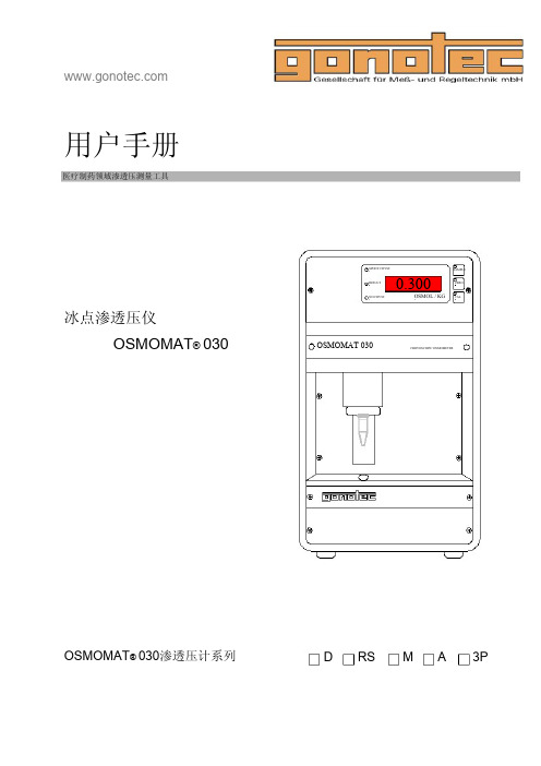
渗透压OSMOMAT 030使用说明
提示用户可能是无效结果
error
警告用户可能会损坏渗透压计或威胁本人身体健康
一般注意事项.
Notes, Safety Notices and Warnings | 3
Table of Contents
目录
标志,注意,警告 ................................................................................................................................................... 3
3.3
一般操作方式............................................................................................................... 17
4
OSMOMAT 030 冰点渗透压仪测量渗透压 ..........................................................................................19
4.3
校准液校准系统 ........................................................................................................... 22
4.4
测量样品溶液............................................................................................................... 24
Lincoln Power TIG 275 焊接机说明书

ProcessesStick, TIGProduct NumberK2619-1K2619-2K2620-1K2618-1 Ready-Pak®Package See back for complete specs© Lincoln Global, Inc. All Rights Reserved.275TIG WELDERSInput Power (Voltage/Phase/Hertz)K2619-1/K2618-1:208/230/460/1/60K2619-2:460/575/1/60K2620-1:220-230/380-400/415/1/50/60Input Current at Rated Output208V:104460V:47220-230V:95575V:38230V:94380-400V:55415V:50Rated Output: Current/Voltage/Duty Cycle275A/31V/40%Weight/Dimensions (H x W x D)397 lbs. (180 kg)31 x 22 x 26 in.(787 x 559 x 660 mm)INPUT OUTPUTK2618-1 Includes:K2619-1Under-Cooler Cart Water Cooler –PH: +1.216-481-8100 • LI NC OL N E L E C TR ICShown K2619-1[ 2]|Precision TIG ®275What Is It?Pulse welding systems vary weld current between peak (high heat) and background current (low heat) levels. Adjusting the pulse frequency controls the level of heat input applied to the weld relative to the weld travel speed.ResultsBetter control of heat input in the weld, resulting in:•Reduced warping and burnthrough on thin materials. •Smaller heat-affected zone – good for thin material.•Smaller bead profile without compromising proper penetration.Easy “Set It/See It” Operation:•Flashing indicator light lets you see the pulse rate before you strike an arc.W e l d i n g C u r r e ntTimePulsed TIG Weld (at 60 amps)Standard TIG Weld (at 60 amps) Smaller HeatAffected ZoneSmaller Bead ProfileMicro-Start ™II Technology aids arc stabilityTHROUGHOUT THE WELD CYCLE – even at the lowest amperage! Micro-Start ™II Technologycontrolled ramp down helps precisely fill the weld crater for quality results.Micro-Start ™II Technology minimizes high frequency and ‘hot starts’ to deliver soft arc starts without arc wandering for AC and DC welding. Arc PerformanceMicro-Start ™Stable, Focused Arc Precise Crater Fill“Set It/See It” Pulse Control — Make attractive and consistent welds!N O WIN C L U D ESf o r A L UM IN U MW E L D INGA CPrecision TIG ®275| [ 3]AC Auto Balance ®Controls —Automatically sets the optimal cleaning vs. penetration level for aluminum welding!What Is It?When aluminum welding, the positive (+) portion of the AC weldingamperage cleans the oxides from the aluminum surface. The negative (-)portion delivers more heat input, increasing penetration level.Patented AC Auto Balance ®automatically sets the ratio of cleaning action (+) versus penetration (-) based on amperage.Manual balance control provides the flexibility to customize the arc to your preference.Easy Operation:•Set it and forget it or override when you choose to customize the settings.More Cleaning (+)Less Cleaning (+)Less Penetration(-)More Penetration (-)W E L D I N G W E L D I N G TIMETIMEMaximum Cleaning SettingMaximum Penetration SettingAuto Balance Setting•Fan-As-Needed (F.A.N.)™minimizes repeated heating and cooling of internal components, keeps dust and dirt build-up to a minimum and saves on electricity costs. •Engineered cooling air routing brings clean air in from the top and exhausts at the bottom to draw and collect less dirt in the machine. •Compare these reliability enhancing design features: — Crimped and soldered power connections.— Wound and varnished electrical coils do not require coil spacers used on competitive models. — Locking tabs on PC board connectors eliminates loose connections.•Tough testing cycles ensure long service — dropping, jerking,rolling, shipping, vibration, resistance to real world extreme conditions, and extended in-service life testing. •CSA C/US certified.•Lincoln three-year warranty on parts and labor.Clean, cool air route shown.Snap-action durable switches make positive mechanical contact to reduce chances ofintermittent contact failure.[ 4]| Precision TIG ®275Shown: K2618-1Water-Cooled Ready-Pak ®PackageTorch Parts Storage Compartment.Optional TIG pulsing helps you make great welds.Water-cooled torch connections with no adapters — side mounted to keep out of the way and protected.Neat/organized cable management with integratedtorch holster.Separate output studs for stick and TIG keep both stick electrode holder and TIG torch connected at the same time — eliminates set-up changeover when switching processes.Easily accessible input voltagereconnect panel.Low-Lift ™ Shielding Gas Bottle Platform.Lockable Undercarriage Storage and Water Cooler Drawers.Reliable Pro-Con Pump.Optional Features:(standard with K2618-1 Water-Cooled Ready-Pak ®Package)Precision TIG ®275| [ 5]Large, well-spaced controls make it easy to view and set upwith gloved hands.SET-UP MENUPress and hold the menu button to display up to seven programmable parameters. The setting of the desired level is displayed, and increasing or decreasing the level setting is easy.The Set-Up Menu includes:Standard•DC TIG Start Modes: High Frequency, Scratch Start, and Touch Start TIG ®.•Adjustable Preflow Time.•Adjustable Start Pulse for Soft or Forceful Starts.With Optional Advanced Control Panel •Adjustable TIG Hot Start.•Adjustable Upslope Time.•Adjustable Stick Hot Start.•Adjustable Stick Arc Force.A)Minimum Output Control & Display Switch (Also displays output voltage)B)Set-Up Menu (see below)C)Digital MeterD)Local/Remote Current Control Switch E)Maximum Output Control F)Post Flow Time G)Thermal Shutdown Light H)Optional Advanced Control Panel 1)Trigger Switch (2-step/4-step)2)Pulse/Spot Time Mode Switch 3)Pulse Frequency Control 4)Pulse % On Time Control 5)Pulse Background Current Control 6)Downslope Time, In Seconds 7)Spot Time I)Polarity Switch J)Power Switch K)AC Balance Control L)Mode SwitchH123 4 & 756BCDEAF G HI J KLC U S T O M E R A S S I S T A N C E P O L I C YThe business of The Lincoln Electric Company ®is manufacturing and selling high quality welding equipment, consumables, and cutting equipment. Our challenge is to meet the needs of our customers and to exceed their expectations. On occasion, purchasers may ask Lincoln Electric for information or advice about their use of our products. Our employees respond to inquiries to the best of their ability based on information provided to them by the customers and the knowledge they may have concerning the application. Our employees, however, are not in a position to verify the information provided or to evaluate the engineering requirements for the particular weldment. Accordingly, Lincoln Electric does not warrant or guarantee or assume any liability with respect to such information or advice. Moreover, the provision of such information or advice does not create, expand, or alter any warranty on our products. Any express or implied warranty that might arise from the information or advice, including any implied warranty of merchantability or any warranty of fitness for any customers’ particular purpose is specifically disclaimed.Lincoln Electric is a responsive manufacturer, but the selection and use of specific products sold by Lincoln Electric is solely within the control of, and remains the sole responsibility of the customer. Many variables beyond the control of Lincoln Electric affect the results obtained in applying these types of fabrication methods and service requirements.Subject to Change – This information is accurate to the best of our knowledge at the time of printing. Please refer to for any updated information.For best welding results with Lincoln Electric equipment,always use Lincoln Electric consumables. Visit for more details.GENERAL OPTIONSAdvanced Control Panel Provides 2/4-step trigger with adjustable Pulser controls and Downslope timer for TIG welding.Also includes adjustable Hot Start and Arc Force internal panel controls for stick welding, and other user selectable features.Order K2621-1Under-Cooler Cart Water Cooler Includes “cooler-in-a-drawer” with hoses and a lockable storage drawer on a dual bottle undercarriage. Two gallon (7.5 ltrs.) capacity.Order K1828-1UndercarriageIncludes a dual bottle rack with chain and front casters, rear wheels and a handle. Order K1869-1Harris ®Argon Flowmeter RegulatorDeluxe flowmeter/regulator. Includes 10 ft. (3.0 m) hose. Order 3100211Work Clamp & Cable Assembly 15 ft. 2/0 cable with 1/2 in. stud lug and work clamp. Order K2150-1STICK OPTIONSAccessory KitFor stick welding. Includes 35 ft.(10.7 m) 2/0 electrode cable with lug, 30 ft. (9.1 m) 2/0 work cable with lugs, headshield, filter plate,work clamp and electrode holder.400 amp capacity.Order K704Accessory KitFor stick welding. Includes 20 ft. (6.1 m) #6 electrode cable with lug,15 ft. (4.6 m) #6 work cable with lugs, headshield, filter plate, work clamp, electrode holder and sample pack of mild steel electrode. 150amp capacity.Order K875Remote Output ControlConsists of a control box with choice of two cable lengths. Permits remote adjustment of output. 6 pin connection.Order K857for 25 ft. (7.6 m)Order K857-1for 100 ft. (30.5 m) TIG OPTIONSMagnum®Pro-Torch™TIG TorchesA full line of air-cooled and water-cooled torches available.Request publication E12.150PTA-26 One-Cable AdapterAdapts the 7/8 in. PTA-26 fitting tothe 5/8 in. gas and powerconnection on machine. Order K2166-1PTA-9, -17 One-Cable Adapter Adapts the 3/8 in. PTA-9 or -17fitting to the 5/8 in. gas and power connection on machine.Order K2166-3PTA-9, PTA-17, PTA-26 Two-Cable AdapterConverts the 7/8 in. water andpower connection on the machine to a 1/2 in. output stud for use with a two-cable air-cooled TIG torch.Order K2166-2Foot Amptrol ™Varies current for making critical TIG welds. Depress pedal to increase current. Depressing pedal fullyachieves maximum set current. Fully raising the pedal finishes the weld and starts the afterflow cycle.Includes 25 ft. (7.6 m) control cable.6-pin plug connection.Order K870Hand Amptrol ™Provides 25 ft. (7.6 m) of remote current control for TIG welding (6 pin plug connection). Velcro straps secure torch.Order K963-3(One size fits all Pro-Torch ™TIG Torches.)Arc Start SwitchNeeded if an Amptrol ™is not used when TIG welding. Comes with a 25ft. (7.6 m) cable. Attaches to the TIG torch for convenient finger control. 6-pin plug connection. Order K814Cut Length Consumables TIG welding filler metals are available for welding stainless steel, mild steel, aluminum and copper alloys.See publication C1.10。
教室音频系统安装及操作手册说明书
Classroom Audio System教室音频系统 Installation and Operating Manual安装及操作手册V 1.3重要的安全说明重要的安全说明1. 在安装和使用设备前请先仔细阅读本安全操作规程。
2. 请保存好您的安全操作指南便于以后作参考用。
3. 请遵守所有设备操作指南中的“警告”事项。
4. 须遵守各项操作指南中的规章原则。
5. 清洁设备:清洁设备之前,请先关掉电源,从插座中拔出设备插头,将各连接的系统单元拆卸出来,清洁时请用干燥的软布擦拭。
6. 未经生产厂家同意,不要使用任何不匹配的附件配置,这都有可能引起危险事故。
7. 勿将设备置于潮湿或靠近热源的地方,以免发生危险。
8. 设备不应遭受水滴或水溅,不应放置诸如花瓶一类装满液体的物品。
9. 电源插头作为断接装置,应便于操作。
10. 设备应可靠连接到带保护接地的电网电源输出插座上。
11. 勿将设备放置在不稳固的台面上;在运输过程中避免设备遭受强烈振动而引起损坏,建议在运输前选用合适的包装或使用原包装。
12. 请勿阻塞设备上的通风开口,并保持室内的空气通畅,便于设备的维护。
13. 供电电压:AC 100 V-240 V 50 Hz/ 60 Hz14. 设备连接所需要的延长电缆线请绕道穿行,勿有重物挤压,这样能有效维护系统的正常工作。
15. 每套系统中所连接的接收器不得超过规定数量,否则可能会导致整个系统中设备的异常工作,如有特殊要求请与距离您最近的深圳台电售后服务中心取得联系。
16. 确保设备不被任意拆开机壳,也不允许任何硬质导体或液态物质残留在机壳内。
17. 设备有需要维护时,不要自行拆卸,请及时与距离您最近的深圳台电售后服务中心取得联系。
18. 所有TAIDEN产品将提供一定期限(详见保修卡)免费保修,但人为损坏除外,例如:A. 设备因人为作用被摔坏;B. 因操作员操作不当而导致设备受损;C. 自行拆卸后而导致部分设备零件受损或丢失。
科尔摩根AKM 同步伺服电机 选型指南说明书
K O L L M O R G E N | A K o l l m o r g e n C O M PA N Y欢迎来到科尔摩根官方微信科尔摩根3目录u AKM ™ 同步伺服电机4u AKD ™ 伺服驱动器8u AKM ™ 各种选件12u AKM ™ 防水型和食品级防水型电机13u AKM ™ 系统综述14u AKM ™ 图纸和性能数据AKM1x 16AKM2x 20AKM3x24AKM4x 28AKM5x 34AKM6x 40AKM7x 44AKM8x48u L 10 轴承疲劳寿命和轴负载53u 反馈选件56u 抱闸选件60u 伺服电机连接器选件61u 型号命名67u MOTIONEERING ® Online71科尔摩根A K M 同步伺服电机选型指南克服设计、采购和时间障碍科尔摩根明白:帮助原始设备制造商的工程师克服障碍,可以显著提高其工作成效。
因而,我们主要通过如下三种方式来提供帮助:集成标准和定制产品在很多情况下,理想方案都不是一成不变的。
我们拥有专业应用知识,可以根据全面的产品组合来修改标准产品或开发全定制解决方案,从而为设计奠定良好的基础。
提供运动控制解决方案而不仅仅是部件在各公司减少供应商数量和工程人力的过程中,他们需要一家能够提供多种集成解决方案的全系统供应商。
科尔摩根就采用了全面响应模式,为客户提供全套解决方案,这些方案将编程软件、工程服务以及同类优秀的运动控制部件结合起来。
覆盖全球我们在美洲、欧洲、中东和亚洲拥有众多直销、工程支持单位、生产工厂以及分销商,临近全球各地的原始设备制造商。
这种便利优势可以加速我们的供货过程,根据客户需要随时随地供货。
财务和运营稳定性科尔摩根隶属于Fortive 公司。
Fortive 业务系统是推动Fortive 各部门发展的一个关键力量。
该系统采用“不断改善”(Kaizen )原理。
由高素质人才构成的多学科团队使用世界级的工具对过程进行评估,并制定相关计划以达到卓越的性能。
2SK2869中文资料
0.8
0.6 I D = 15 A
0.4 10 A
0.2
5A
0
4
8
12 16 20
Gate to Source Voltage V GS (V)
Drain to Source On State Resistance R DS(on) ( Ω )
2SK2869
Static Drain to Source on State Resistance vs. Drain Current
IF = 20A, VGS = 0
IF = 20A, VGS = 0 diF/ dt = 50A/µs
3
Channel Dissipation Pch (W)
2SK2869
Main Characteristics
Power vs. Temperature Derating 40
30
20
10
0
50
100
Test Conditions ID = 10mA, VGS = 0
IG = ±100µA, VDS = 0
VGS = ±16V, VDS = 0 VDS = 60 V, VGS = 0
ID = 1mA, VDS = 10V ID = 10A, VGS = 10V*1 ID = 10A, VGS = 4V*1 ID = 10A, VDS = 10V*1 VDS = 10V VGS = 0 f = 1MHz ID = 10A, VGS = 10V RL = 3Ω
5
2SK2869
Reverse Recovery Time trr (ns)
1000 500
Body to Drain Diode Reverse Recovery Time
- 1、下载文档前请自行甄别文档内容的完整性,平台不提供额外的编辑、内容补充、找答案等附加服务。
- 2、"仅部分预览"的文档,不可在线预览部分如存在完整性等问题,可反馈申请退款(可完整预览的文档不适用该条件!)。
- 3、如文档侵犯您的权益,请联系客服反馈,我们会尽快为您处理(人工客服工作时间:9:00-18:30)。
Product Specification(Preliminary)Part Name:OEL Display ModuleCustomer Part ID:WiseChip Part ID: UG-2864ASWPG01Doc No.:SAS1-090BH-ACustomer:Approved byTopwin international corp.,limitedApproved byTopwin international corp.,limitedRevised HistoryPart Number RevisionUG-2864ASWPG01A NewRevision ContentRevised on June 6, 2012iTopwin international corp.,limitedContentsRevision History ................................................................................................................................i Contents...........................................................................................................................................ii 1. Basic Specifications................................................................................................................ 1~51.1 Display Specifications ................................................................................................................. 1 1.2 Mechanical Specifications............................................................................................................ 1 1.3 Active Area / Memory Mapping & Pixel Construction ...................................................................... 1 1.4 Mechanical Drawing.................................................................................................................... 2 1.5 Pin Definition ............................................................................................................................. 3 1.6 Block Diagram............................................................................................................................ 5 2. Absolute Maximum Ratings ........................................................................................................6 3. Optics & Electrical Characteristics ....................................................................................... 7~11 3.1 Optics Characteristics.................................................................................................................. 7 3.2 DC Characteristics ...................................................................................................................... 7 3.3 AC Characteristics....................................................................................................................... 83.3.1 68XX-Series MPU Parallel Interface Timing Characteristics.................................................... 8 3.3.2 80XX-Series MPU Parallel Interface Timing Characteristics.................................................... 9 3.3.3 Serial Interface Timing Characteristics .............................................................................. 10 3.3.4 I2C Interface Timing Characteristics ................................................................................. 11 4. Functional Specification.....................................................................................................12~14 4.1 Commands .............................................................................................................................. 12 4.2 Power down and Power up Sequence......................................................................................... 12 4.2.1 Power up Sequence ........................................................................................................ 12 4.2.2 Power down Sequence .................................................................................................... 12 4.3 Reset Circuit ............................................................................................................................ 12 4.4 Actual Application Example........................................................................................................ 13 5. Reliability ..................................................................................................................................15 5.1 Contents of Reliability Tests ...................................................................................................... 15 5.2 Failure Check Standard ............................................................................................................. 15 6. Outgoing Quality Control Specifications ............................................................................16~19 6.1 Environment Required .............................................................................................................. 16 6.2 Sampling Plan .......................................................................................................................... 16 6.3 Criteria & Acceptable Quality Level............................................................................................. 16 6.3.1 Cosmetic Check (Display Off) in Non-Active Area............................................................... 16 6.3.2 Cosmetic Check (Display Off) in Active Area...................................................................... 18 6.3.3 Pattern Check (Display On) in Active Area......................................................................... 19 7. Package Specifications..............................................................................................................20 8. Precautions When Using These OEL Display Modules .......................................................21~23 8.1 Handling Precautions ................................................................................................................ 21 8.2 Storage Precautions.................................................................................................................. 21 8.3 Designing Precautions............................................................................................................... 22 8.4 Precautions when disposing of the OEL display modules .............................................................. 22 8.5 Other Precautions..................................................................................................................... 22 Warranty ........................................................................................................................................23 Notice .............................................................................................................................................23iiTopwin international corp.,limited1. Basic Specifications1.1 Display Specifications1) Display Mode: 2) Display Color: 3) Drive Duty:Passive Matrix Monochrome (White) 1/64 Duty1.2 Mechanical Specifications1) Outline Drawing: 2) Number of Pixels: 3) Panel Size: 4) Active Area: 5) Pixel Pitch: 6) Pixel Size: 7) Weight:According to the annexed outline drawing 128 × 64 60.50 × 37.00 × 2.00 (mm) 55.01 × 27.49 (mm) 0.43 × 0.43 (mm) 0.40 × 0.40 (mm) 8.60 (g)1.3 Active Area / Memory Mapping & Pixel Construction P0.43x128-0.03=55.01 (A/A)(0, 0)"A"Driver IC Memory Mapping (Full 128 x 64)P0.43x64-0.03=27.49 (A/A)Segment 127( Column 1 )Common 32( Row 63 )Common 63( Row 1 )0.43 0.4Detail "A" Scale (10:1)Segment 0( Column 128 )Common 0( Row 64 )Common 31( Row 2 )(127, 63)10.40.43Topwin international corp.,limited1.4 Mechanical Drawing0.5±0.5 (1.75) (2.75)"A"60.5±0.2 (Panel Size) 60.5±0.2 (Cap Size)59.5 (Polarizer) 57.01 (V/A)P0.43x128-0.03=55.01 (A/A)105Remove Tape t=0.15mm Max2±0.1(4.35)ItemDateA20120531Remark Original Drawing(2.08) (1.08) 0.5±0.58Polarizer t=0.2mmP0.43x64-0.03=27.49 (A/A) 29.49 (V/A) 31.5 (Polarizer)32.408±0.2 (Cap Size) 37±0.2 (Panel Size) (73)(34) (1.35)Active Area 2.42" 128 x 64 PixelsSegment 127 ( Column 1 )Common 32 ( Row 63 )Common 63 ( Row 1 )Segment 0 ( Column 128 )Common 0 ( Row 64 )Common 31 ( Row 2 )GlueProtective Tape 15x3.5x0.05mm8.5±0.12-φ0.8±0.125±0.2 36±0.310.4±0.12-φ 1±0.11243±0.3 6±0.2N.C. (GND) VLSS VSS N.C. VDD BS1 BS2 CS# RES# D/C# R/W# E/ R D# D0 D1 D2 D3 D4 D5 D6 D7 IREF VCOMH VCC N.C. (GND)Notes:W=0.35±0.030.5±0.1P1.0x(31-1)=11.5±0.05(24)12.5±0.21. Color: White 2. Driver IC: SSD1309 3. FPC Number: UT-0205-P05 4. Interface:8-bit 68XX/80XX Parallel, 4-wire SPI, I2C 5. General Tolerance: ±0.30 6. The total thickness (2.10 Max) is without polarizer protective film & remove tape.The actual assembled total thickness with above materials should be 2.35 Max.(2.3)Customer Approval Signature0.43 0.40.4 0.434.5±0.5 (Stiffener) Contact Side0.3±0.03Detail "A" Scale (10:1)Topwin international corp.,limitedUnless Otherwise SpecifiedUnitmmGeneral RoughnessToleranceDimension ±0.3Angle±1TitleBy DateUG-2864ASWPG01 Folding Type OEL Display Module Pixel Number: 128 x 64, Monochrome, COG PackageDrawn Dora Yang 20120531E.E. Ting-Kuo Hu20120531Panel / E. Ivy Lo20120531P.M. Tiffany Hsu 20120531PinSymbol1N.C. (GND)2VLSS3VSS4N.C.5VDD6BS17BS28CS#9RES#10D/C#11R/W#12E/RD#13D014D115D216D317D418D519D620D721IREF22VCOMH23VCC24N.C. (GND)Drawing Number DMX2864CNGFBHMaterialRev. ASoda Lime / PolyimideScale Sheet Size 1:1 1 of 1 A32Topwin international corp.,limited1.5 Pin DefinitionPin Number SymbolPower Supply5VDD3VSS23 2 Driver 21VCC VLSSIREF22 InterfaceVCOMH6BS17BS29RES#8CS#10D/C#12E/RD#11R/W#I/OFunctionPPower Supply for Logic Circuit This is a voltage supply pin. It must be connected to external source.Ground of Logic CircuitP This is a ground pin. It also acts as a reference for the logic pins. It must beconnected to external ground.Power Supply for OEL PanelP This is the most positive voltage supply pin of the chip. It must be suppliedexternally.PGround of Analog Circuit This is an analog ground pin. It should be connected to VSS externally.Current Reference for Brightness AdjustmentI This pin is segment current reference pin. A resistor should be connectedbetween this pin and VSS. Set the current at 10μA.Voltage Output High Level for COM SignalO This pin is the input pin for the voltage output high level for COM signals. Acapacitor should be connected between this pin and VSS.Communicating Protocol SelectThese pins are MCU interface selection input. See the following table:II2CBS1BS2104-wire Serial008-bit 68XX Parallel018-bit 80XX Parallel11Power Reset for Controller and DriverI This pin is reset signal input. When the pin is low, initialization of the chip isexecuted. Keep this pin pull high during normal operation.Chip SelectI This pin is the chip select input. The chip is enabled for MCU communication onlywhen CS# is pulled low.Data/Command ControlThis pin is Data/Command control pin. When the pin is pulled high, the input atD7~D0 will be interpreted as display data. When the pin is pulled low, the inputat D7~D0 will be transferred to the command register.IWhen the pin is pulled high and serial interface mode is selected, the data at SDIN will be interpreted as data. When it is pulled low, the data at SDIN will betransferred to the command register. In I2C mode, this pin acts as SA0 for slaveaddress selection.For detail relationship to MCU interface signals, please refer to the TimingCharacteristics Diagrams.Read/Write Enable or ReadThis pin is MCU interface input. When interfacing to a 68XX-seriesmicroprocessor, this pin will be used as the Enable (E) signal. Read/write operationIis initiated when this pin is pulled high and the CS# is pulled low. When connecting to an 80XX-microprocessor, this pin receives the Read (RD#)signal. Data read operation is initiated when this pin is pulled low and CS# ispulled low. When serial or I2C mode is selected, this pin must be connected to VSS.Read/Write Select or WriteThis pin is MCU interface input. When interfacing to a 68XX-seriesmicroprocessor, this pin will be used as Read/Write (R/W#) selection input. PullIthis pin to “High” for read mode and pull it to “Low” for write mode. When 80XX interface mode is selected, this pin will be the Write (WR#) input.Data write operation is initiated when this pin is pulled low and the CS# is pulledlow. When serial or I2C mode is selected, this pin must be connected to VSS.3Topwin international corp.,limited1.5 Pin Definition (Continued)Pin Number Symbol I/OFunctionInterface (Continued)13~20D0~D7Reserve 41, 24N.C. N.C. (GND)Host Data Input/Output BusThese pins are 8-bit bi-directional data bus to be connected to themicroprocessor’s data bus. When serial mode is selected, D1 will be the serialI/O data input SDIN and D0 will be the serial clock input SCLK. When I2C mode isselected, D2, D1 should be tired together and serve as SDAOUT, SDAIN in application and D0 is the serial clock input, SCL.Unused pins must be connected to VSS except for D2 in serial mode.-Reserved Pin The N.C. pin between function pins is reserved for compatible and flexible design.Reserved Pin (Supporting Pin)- The supporting pins can reduce the influences from stresses on the function pins.These pins must be connected to external ground as the ESD protection circuit.4Topwin international corp.,limited1.6 Block DiagramActive Area 2.42" 128 x 64 PixelsCommon 63 Common 32 Segment 127 Segment 0 Common 0 Common 31~~~~~SSD1309VLSS VSS VDD BS1 BS2 CS# RES# D/C# R/W# E/RD# D0 D7 IREF VCOMH VCC~C1C2R1C5C3C4MCU Interface Selection:BS1 and BS2Pins connected to MCU interface: D7~D0, E/RD#, R/W#, D/C#, RES#, and CS#C1, C3: 0.1μF C2: 4.7μF C4: 10μF C5: 4.7μF / 25V Tantalum Capacitor R1: 910kΩ, R1 = (Voltage at IREF - BGGND) / IREF5Topwin international corp.,limited2. Absolute Maximum RatingsParameterSymbolMinMaxUnitNotesSupply Voltage for Logic Supply Voltage for DisplayOperating Temperature Storage Temperature Life Time (80 cd/m2) Life Time (60 cd/m2)VDD-0.34V1, 2VCC015V1, 2TOP-4070°C3TSTG-4085°C330,000-hour450,000-hour4Note 1: All the above voltages are on the basis of “VSS = 0V”. Note 2: When this module is used beyond the above absolute maximum ratings, permanent breakage of themodule may occur. Also, for normal operations, it is desirable to use this module under the conditions according to Section 3. “Optics & Electrical Characteristics”. If this module is used beyond these conditions, malfunctioning of the module can occur and the reliability of the module may deteriorate. Note 3: The defined temperature ranges do not include the polarizer. The maximum withstood temperature of the polarizer should be 80°C. Note 4: VCC = 13.0V, Ta = 25°C, 50% Checkerboard. Software configuration follows Section 4.4 Initialization. End of lifetime is specified as 50% of initial brightness reached. The average operating lifetime at room temperature is estimated by the accelerated operation at high temperature conditions.6Topwin international corp.,limited3. Optics & Electrical Characteristics3.1 Optics CharacteristicsCharacteristicsSymbolConditionsBrightnessLbrC.I.E. (White)(x) (y)Dark Room ContrastCRNote 5 C.I.E. 1931Viewing Angle* Optical measurement taken at VDD = 2.8V, VCC = 13.0V. Software configuration follows Section 4.4 Initialization.Min Typ Max6080-0.25 0.29 0.33 0.27 0.31 0.35- >10,000:1 --Free-Unit cd/m2degree3.2 DC CharacteristicsCharacteristicsSymbolConditionsMin Typ Max UnitSupply Voltage for Logic Supply Voltage for DisplayHigh Level Input Low Level Input High Level Output Low Level Output Operating Current for VDDVDD1.652.83.3VVCCNote 512.5 13.0 13.5VVIH IOUT = 100μA, 3.3MHz 0.8×VDD-VDDVVIL IOUT = 100μA, 3.3MHz 0-0.2×VDDVVOH IOUT = 100μA, 3.3MHz 0.9×VDD-VDDVVOL IOUT = 100μA, 3.3MHz 0-0.1×VDDVIDD-180300μANote 6-18.5 23.1 mAOperating Current for VCCICCNote 7-27.1 33.9 mANote 8-42.3 52.9 mASleep Mode Current for VDD IDD, SLEEP-15μASleep Mode Current for VCC ICC, SLEEP-210μANote 5: Brightness (Lbr) and Supply Voltage for Display (VCC) are subject to the change of the panel characteristics and the customer’s request.Note 6: VDD = 2.8V, VCC = 13.0V, 30% Display Area Turn on. Note 7: VDD = 2.8V, VCC = 13.0V, 50% Display Area Turn on. Note 8: VDD = 2.8V, VCC = 13.0V, 100% Display Area Turn on.* Software configuration follows Section 4.4 Initialization.7Topwin international corp.,limited3.3 AC Characteristics 3.3.1 68XX-Series MPU Parallel Interface Timing Characteristics:Symbol Descriptiontcycle tAS tAH tDW tDSW tDHW tDHR tOH tACCPWCSLClock Cycle Time Address Setup Time Address Hold Time Data Write Time Write Data Setup Time Write Data Hold Time Read Data Hold Time Output Disable Time Access Time Chip Select Low Pulse Width (Read) Chip Select Low Pulse width (Write)PWCSHChip Select High Pulse Width (Read) Chip Select High Pulse Width (Write)tRRise TimetFFall Time* (VDD - VSS = 1.65V to 3.3V, Ta = 25°C)Min Max Unit300-ns20-ns0-ns80-ns40-ns20-ns20-ns-70ns-140ns120-ns6060-ns60-40ns-40ns8Topwin international corp.,limited3.3.2 80XX-Series MPU Parallel Interface Timing Characteristics:Symbol Descriptiontcycle Clock Cycle TimetASAddress Setup TimetAH Address Hold TimetDW Data Write TimetDSW Write Data Setup TimetDHW Write Data Hold TimetDHR Read Data Hold TimetOH Output Disable TimetACC Access TimetPWLR Read Low TimetPWLW Write Low TimetPWHR Read High TimetPWHW Write High TimetCS Chip Select Setup TimetCSH Chip Select Hold Time to Read SignaltCSF Chip Select Hold TimetRRise TimetFFall Time* (VDD - VSS = 1.65V to 3.5V, Ta = 25°C)Min Max Unit300-ns20-ns0-ns70-ns40-ns15-ns20-ns-70ns-140ns120-ns60-ns60-ns60-ns0-ns0-ns20-ns-40ns-40ns( Read Timing )( Write Timing ) 9Topwin international corp.,limited3.3.3 Serial Interface Timing Characteristics:Symbol Descriptiontcycle Clock Cycle TimetASAddress Setup TimetAH Address Hold TimetCSS Chip Select Setup TimetCSH Chip Select Hold TimetDW Data Write TimetDSW Write Data Setup TimetDHW Write Data Hold TimetCLKL Clock Low TimetCLKH Clock High TimetRRise TimetFFall Time* (VDD - VSS = 1.65V to 3.5V, Ta = 25°C)Min Max Unit100-ns15-ns15-ns20-ns50-ns55-ns15-ns15-ns50-ns50-ns-40ns-40ns10Topwin international corp.,limited3.3.4 I2C Interface Timing Characteristics:Symbol Descriptiontcycle Clock Cycle TimetHSTART Start Condition Hold TimeData Hold Time (for “SDAOUT” Pin) tHDData Hold Time (for “SDAIN” Pin)tSD tSSTARTData Setup TimeStart Condition Setup Time (Only relevant for a repeated Start condition)tSSTOP Stop Condition Setup TimetRRise Time for Data and Clock PintFFall Time for Data and Clock PintIDLE Idle Time before a New Transmission can Start* (VDD - VSS = 1.65V to 3.5V, Ta = 25°C)Min Max Unit2.5-μs0.6-μs0-ns300100-ns0.6-μs0.6-μs300ns300ns1.3-μs11Topwin international corp.,limited4. Functional Specification4.1 Commands Refer to the Technical Manual for the SSD13094.2 Power down and Power up SequenceTo protect OEL panel and extend the panel life time, the driver IC power up/down routine should include a delay period between high voltage and low voltage power sources during turn on/off. It gives the OEL panel enough time to complete the action of charge and discharge before/after the operation.4.2.1 Power up Sequence:1. Power up VDD 2. Send Display off command 3. Initialization 4. Clear Screen 5. Power up VCC 6. Delay 100ms(When VCC is stable) 7. Send Display on command4.2.2 Power down Sequence:1. Send Display off command 2. Power down VCC 3. Delay 100ms(When VCC is reach 0 and panel is completely discharges) 4. Power down VDDVCC VDD VSS/GroundVCC VDD VSS/GroundVDD on VCC onDisplay onDisplay off VCC offVDD offNote 9:1) Since an ESD protection circuit is connected between VDD and VCC inside the driver IC, VCC becomes lower than VDD whenever VDD is ON and VCC is OFF.2) VCC should be kept float (disable) when it is OFF. 3) Power Pins (VDD, VCC) can never be pulled to ground under any circumstance. 4) VDD should not be power down before VCC power down.4.3 Reset CircuitWhen RES# input is low, the chip is initialized with the following status: 1. Display is OFF 2. 128×64 Display Mode 3. Normal segment and display data column and row address mapping (SEG0 mapped to columnaddress 00h and COM0 mapped to row address 00h) 4. Shift register data clear in serial interface 5. Display start line is set at display RAM address 0 6. Column address counter is set at 0 7. Normal scan direction of the COM outputs 8. Contrast control register is set at 7Fh 9. Normal display mode (Equivalent to A4h command)12Topwin international corp.,limited4.4 Actual Application Example Command usage and explanation of an actual example <Power up Sequence>VDD/VCC off StatePower up VDD (RES# as Low State)Power Stabilized (Delay Recommended)Set RES# as High (3μs Delay Minimum)Initialized State (Parameters as Default)Command Lock 0xFD, 0x12Set Display Off 0xAEInitial Settings ConfigurationSet Display Clock Divide Ratio/Oscillator Frequency 0xD5, 0xA0Set Multiplex Ratio 0xA8, 0x3FSet Display Offset 0xD3, 0x00Set Display Start Line 0x40Set Segment Re-Map 0xA1Set COM Output Scan Direction 0xC8Set COM Pins Hardware Configuration 0xDA, 0x12Set Current Control 0x81, 0xDFSet Pre-Charge Period 0xD9, 0x82Set VCOMH Deselect Level 0xDB, 0x34Set Entire Display On/Off 0xA4Set Normal/Inverse Display 0xA6Clear ScreenPower up VCC & Stabilized (Delay Recommended)Set Display On 0xAF(100ms Delay Recommended)Display Data SentIf the noise is accidentally occurred at the displaying window during the operation, please reset the display in order to recover the display function.<Power down Sequence>Normal OperationSet Display Off 0xAEPower down VCC (100ms Delay Recommended)Power down VDDVDD/VCC off State13Topwin international corp.,limited<Entering Sleep Mode>Normal OperationSet Display Off 0xAEPower down VCC Sleep Mode<Exiting Sleep Mode>Sleep ModePower up VCC & Stabilized (Delay Recommended)Set Display On 0xAF(100ms Delay Recommended)Normal Operation14Topwin international corp.,limited5. Reliability5.1 Contents of Reliability TestsItemConditionsHigh Temperature Operation70°C, 240 hrsLow Temperature Operation-40°C, 240 hrsHigh Temperature Storage85°C, 240 hrsLow Temperature Storage-40°C, 240 hrsHigh Temperature/Humidity Operation60°C, 90% RH, 120 hrsThermal Shock-40°C ⇔ 85°C, 24 cycles 60 mins dwell* The samples used for the above tests do not include polarizer. * No moisture condensation is observed during tests.CriteriaThe operational functions work.5.2 Failure Check StandardAfter the completion of the described reliability test, the samples were left at room temperature for 2 hrs prior to conducting the failure test at 23±5°C; 55±15% RH.15Topwin international corp.,limited6. Outgoing Quality Control Specifications6.1 Environment RequiredCustomer’s test & measurement are required to be conducted under the following conditions:Temperature:23 ± 5°CHumidity:55 ± 15% RHFluorescent Lamp:30WDistance between the Panel & Lamp:≥ 50cmDistance between the Panel & Eyes of the Inspector: ≥ 30cmFinger glove (or finger cover) must be worn by the inspector.Inspection table or jig must be anti-electrostatic.6.2 Sampling Plan Level II, Normal Inspection, Single Sampling, MIL-STD-105E6.3 Criteria & Acceptable Quality LevelPartition Major MinorAQL 0.65 1.0Definition Defects in Pattern Check (Display On) Defects in Cosmetic Check (Display Off)6.3.1 Cosmetic Check (Display Off) in Non-Active AreaCheck ItemClassificationCriteriaX > 6 mm (Along with Edge) Y > 1 mm (Perpendicular to edge)XPanel General ChippingMinorY XY16Topwin international corp.,limited6.3.1 Cosmetic Check (Display Off) in Non-Active Area (Continued)Check ItemClassificationCriteria Any crack is not allowable.Panel CrackMinorCopper Exposed (Even Pin or Film)Film or Trace DamageMinorNot Allowable by Naked Eye InspectionMinorTerminal Lead Prober MarkAcceptableGlue or Contamination on Pin (Couldn’t Be Removed by Alcohol)MinorInk Marking on Back Side of panel (Exclude on Film)AcceptableIgnore for Any17Topwin international corp.,limited6.3.2 Cosmetic Check (Display Off) in Active AreaIt is recommended to execute in clear room environment (class 10k) if actual in necessary.Check ItemAny Dirt & Scratch on Polarizer’s Protective FilmClassification AcceptableScratches, Fiber, Line-Shape Defect (On Polarizer)MinorDirt, Black Spot, Foreign Material, (On Polarizer)MinorCriteriaIgnore for not Affect the PolarizerW ≤ 0.1IgnoreW > 0.1, L ≤ 2n≤1L>2n=0Φ ≤ 0.1Ignore0.1 < Φ ≤ 0.25n≤10.25 < Φn=0Φ ≤ 0.5 Î Ignore if no Influence on Display0.5 < Φn=0Dent, Bubbles, White spot (Any Transparent Spot on Polarizer)MinorFingerprint, Flow Mark (On Polarizer)Minor* Protective film should not be tear off when cosmetic check. ** Definition of W & L & Φ (Unit: mm): Φ = (a + b) / 2LNot Allowableb: Minor Axis Wa: Major Axis18。