2SC3187中文资料
2SC3307中文资料
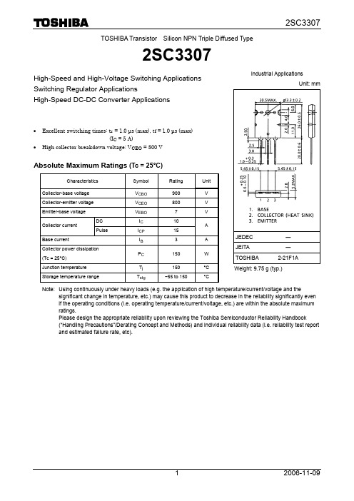
TOSHIBA Transistor Silicon NPN Triple Diffused Type2SC3307High-Speed and High-Voltage Switching Applications Switching Regulator ApplicationsHigh-Speed DC-DC Converter Applications• Excellent switching times: t r = 1.0 μs (max), t f = 1.0 μs (max)(I C = 5 A)• High collector breakdown voltage: V CEO = 800 VAbsolute Maximum Ratings (Tc = 25°C)Characteristics Symbol Rating UnitCollector-base voltage V CBO 900 V Collector-emitter voltage V CEO 800 V Emitter-base voltage V EBO7 VDC I C 10Collector current Pulse I CP 15ABase currentI B 3 A Collector power dissipation (Tc = 25°C)P C 150 W Junction temperature T j 150 °C Storage temperature rangeT stg−55 to 150°CNote: Using continuously under heavy loads (e.g. the application of high temperature/current/voltage and thesignificant change in temperature, etc.) may cause this product to decrease in the reliability significantly even if the operating conditions (i.e. operating temperature/current/voltage, etc.) are within the absolute maximum ratings.Please design the appropriate reliability upon reviewing the Toshiba Semiconductor Reliability Handbook(“Handling Precautions”/Derating Concept and Methods) and individual reliability data (i.e. reliability test report and estimated failure rate, etc).Industrial ApplicationsUnit: mmJEDEC ― JEITA―TOSHIBA 2-21F1AWeight: 9.75 g (typ.)Electrical Characteristics (Tc = 25°C)Markinglead (Pb)-free finish.Collector-emitter voltage V CE (V)I C – V CECo l l e ct o r c u r r e n tI C (A )Collector current I C (A)h FE – I CD C c u r r e n t g a in h F ECollector current I C (A)V CE (sat) – I CC o l l e c t o r -e m i t t e r s a t u r a t i on v o l t a g eV C E (s a t) (V )Base-emitter voltage V BE (V)I C – V BEC ol l ec t o r c u r r e n t IC (A )Collector current I C (A)V BE (sat) – I CB a s e -e m i t t e r s a t u r a t i on v o l t a g e V B E(s a t ) (V )Collector current I C (A)Switching CharacteristicsS w i t c h i n g t i m e (μs )0.030.1 0.3 1 100.013 0.003 0.03 0.1 0.3 1 100 4 8 2 6 100.0030.030.1 0.3 1 100.01 3Collector-emitter voltage V CE (V)Safe Operating AreaC ol l ec t or cu r r e ntIC(A )3 30 100 300 100010 Pulse width t w (s)r th – t wT r a n s i e n t t h e r m a l r e s i s t a n c e r t h (°C /W )RESTRICTIONS ON PRODUCT USE20070701-EN •The information contained herein is subject to change without notice.•TOSHIBA is continually working to improve the quality and reliability of its products. Nevertheless, semiconductor devices in general can malfunction or fail due to their inherent electrical sensitivity and vulnerability to physical stress. It is the responsibility of the buyer, when utilizing TOSHIBA products, to comply with the standards of safety in making a safe design for the entire system, and to avoid situations in which a malfunction or failure of such TOSHIBA products could cause loss of human life, bodily injury or damage to property.In developing your designs, please ensure that TOSHIBA products are used within specified operating ranges as set forth in the most recent TOSHIBA products specifications. Also, please keep in mind the precautions and conditions set forth in the “Handling Guide for Semiconductor Devices,” or “TOSHIBA Semiconductor Reliability Handbook” etc.• The TOSHIBA products listed in this document are intended for usage in general electronics applications (computer, personal equipment, office equipment, measuring equipment, industrial robotics, domestic appliances, etc.).These TOSHIBA products are neither intended nor warranted for usage in equipment that requires extraordinarily high quality and/or reliability or a malfunction or failure of which may cause loss of human life or bodily injury (“Unintended Usage”). Unintended Usage include atomic energy control instruments, airplane or spaceship instruments, transportation instruments, traffic signal instruments, combustion control instruments, medical instruments, all types of safety devices, etc.. Unintended Usage of TOSHIBA products listed in his document shall be made at the customer’s own risk.•The products described in this document shall not be used or embedded to any downstream products of which manufacture, use and/or sale are prohibited under any applicable laws and regulations.• The information contained herein is presented only as a guide for the applications of our products. No responsibility is assumed by TOSHIBA for any infringements of patents or other rights of the third parties which may result from its use. No license is granted by implication or otherwise under any patents or other rights of TOSHIBA or the third parties.• Please contact your sales representative for product-by-product details in this document regarding RoHS compatibility. Please use these products in this document in compliance with all applicable laws and regulations that regulate the inclusion or use of controlled substances. Toshiba assumes no liability for damage or losses occurring as a result of noncompliance with applicable laws and regulations.。
2SC4617贴片三极管 SOT-523三极管封装2SC4617参数
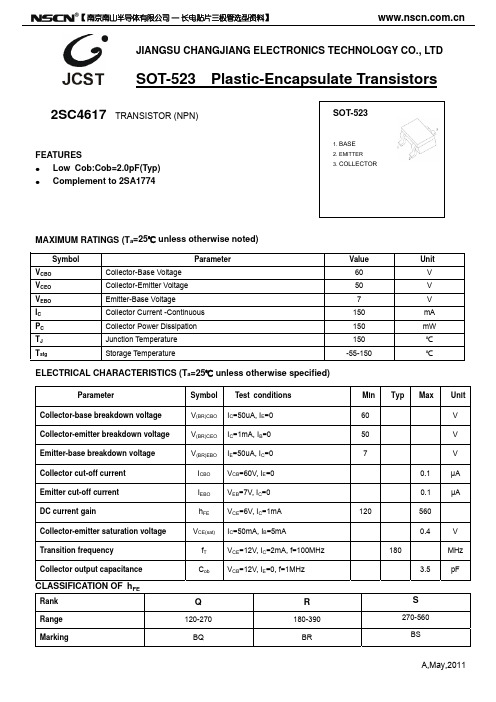
ELECTRICAL CHARACTERISTICS (Ta=25℃ unless otherwise specified)
Parameter Collector-base breakdown voltage Collector-emitter breakdown voltage Emitter-base breakdown voltage Collector cut-off current Emitter cut-off current DC current gain Collector-emitter saturation voltage Transition frequency Collector output capacitance Symbol V(BR)CBO V(BR)CEO V(BR)EBO ICBO IEBO hFE VCE(sat) fT Cob Test conditions IC=50uA, IE=0 IC=1mA, IB=0 IE=50uA, IC=0 VCB=60V, IE=0 VEB=7V, IC=0 VCE=6V, IC=1mA IC=50mA, IB=5mA VCE=12V, IC=2mA, f=100MHz VCB=12V, IE=0, f=1MHz 180 3.5 120 Min 60 50 7 0.1 0.1 560 0.4 V MHz pF Typ Max Unit V V V μA μA
IC
COMMON EMITTER IC/IB=10
30
——
VBE
VCE=6V
COLLECTOR-EMITTER SATURATION VOLTAGE VCEsat (mV)
300
(mA)
10
COLLCETOR CURRENTIC1 Nhomakorabea03
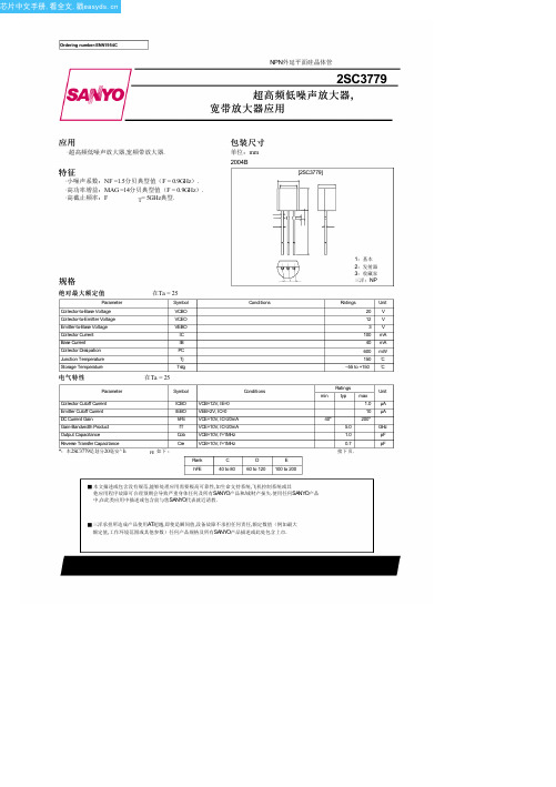
2SC3779中文资料(sanyo)中文数据手册「EasyDatasheet - 矽搜」
三洋电机有限公司努力为客户提供高品质高可靠性产品.但是,所有半导体产品都有一定失效概率. 这是可能,这些失败概率会引起事故或事件,危及人生命,这可能会导致冒烟或起火,或可能造成损害 其他财产.当设计产品时,必须采用安全指标,这样就不会发生这类事故或事件.这些措施包括但不 限于:防护护电路和错误预防电路,用于安全设计,多余设计和结构设计.
在任何或所有SANYO产品(包括技术参数和服务)描述或此处包含在任何适用当地出口管制 法律和法规,此类产品控制不得expor特德未取得有关当局exporT许可证情况下按照上述法律.
本出版物任何部分进行复制或以任何形式或通过任何手段,电子或机械,包括影印和录制,或任何信 息存储和检索系统,或者以其他方式传播,而不三洋电机有限公司事先书面许可, . 任何和所有描述或所载资料如有恕不另行通知更改因产品/技术提高等.当设计产品时,指是 "交付规范"为SANYO产品,你打算使用. 信息(包括电路图和电路参数),例如只;它不是批量生产防护证. SANYO任何信息都是准确可靠 ,但不防护证是对其使用武力或以知识产权或其它第三方权利任何侵犯提出或暗示.
Symbol ICBO IEBO hFE fT Cob Cre
FE 如下 :
Conditions VCB=12V, IE=0 VEB=2V, IC=0 VCE=10V, IC=20mA VCE=10V, IC=20mA VCB=10V, f=1MHz VCB=10V, f=1MHz Rank hFE C 40 to 80 D 60 to 120 E 100 to 200
1:基本 2:发射器 3:收藏家 三洋:NP 在Ta = 25
Symbol VCBO VCEO VEBO IC IB PC Tj Tstg Conditions Ratings 20 12 3 100 40 600 150 –55 to +150 Unit V V V mA mA mW ˚C ˚C
2SC1846中文资料

2SC3507中文资料

Switching time ton,tstg,tf (µs)
3
Collector current IC (A)
tstg 1
10
0.3
ton tf
0.1 Pulsed tw=1ms Duty cycle=1% IC/IB=5 (2IB1=–IB2) VCC=250V TC=25˚C 0 1 2 3 4 5 6 7
2SC3507
IC — VCE
Collector to emitter saturation voltage VCE(sat) (V)
100 IC/IB=5 30 10 3 TC=100˚C 1 25˚C 0.3 –25˚C 0.1 0.03 0.01 0.01 0.03
VCE(sat) — IC
Collector power dissipation PC (W)
0.7
15.0±0.3 11.0±0.2
5.0±0.2 3.2
φ3.2±0.1
2.0±0.2 2.0±0.1 1.1±0.1 5.45±0.3 10.9±0.5 1 2 3 0.6±0.2
1:Base 2:Collector 3:Emitter TOP–3 Full Pack Package(a)
s Electrical Characteristics
Thermal resistance Rth(t) (˚C/W)
102 (1)
10
(2)
1
10–1 10–4
10–3
10–2
10–1
10
102
103
104
Time t (s)
3
1000 VCE=5V 300 100 30 10 3 1 0.3 0.1 0.01 0.03
2SK2487中文资料

Document No. D10283EJ1V0DS00 (1st edition)Date Published August 1995 PPrinted in Japan©19952SK24872ELECTRICAL CHARACTERISTICS (T A = 25 ˚C)The application circuits and their parameters are for references only and are not intended for use in actual design-in's.Test Circuit 3 Gate ChargeV GS PGTest Circuit 1 Avalanche CapabilityLTest Circuit 2 Switching TimePG.L DDt = 1 usDuty Cycle ≤ 1 %2SK24873TYPICAL CHARACTERISTICS (T A = 25 ˚C)FORWARD BIAS SAFE OPERATING AREAI D - D r a i n C u r r e n t - ADRAIN CURRENT vs.DRAIN TO SOURCE VOLTAGEV DS - Drain to Source Voltage - VI D - D r a i n C u r r e n t - AV GS - Gate to Source Voltage - VI D - D r a i n C u r r e n t - A0.1TOTAL POWER DISSIPATION vs.CASE TEMPERATURET C - Case Temperature - ˚C P T - T o t a l P o w e r D i s s i p a t i o n - W20406080100120140160140120100806040200.11101000101.01010020DERATING FACTOR OF FORWARD BIAS SAFE OPERATING AREAT C - Case Temperature - ˚C d T - P e r c e n t a g e o f R a t e d P o w e r - %020406080100120140160204060801002SK24874TRANSIENT THERMAL RESISTANCE vs. PULSE WIDTHPW - Pulse Width - sr t h (t ) - T r a n s i e n t T h e r m a l R e s i s t a n c e - ˚C /WFORWARD TRANSFER ADMITTANCE vs.DRAIN CURRENT| y f s| - F o r w a r d T r a n s f e r A d m i t t a n c e - SDRAIN TO SOURCE ON-STATE RESISTANCE vs.GATE TO SOURCE VOLTAGEV GS - Gate to Source Voltage - V R D S (o n ) - D r a i n t o S o u r c e O n -S t a t e R e s i s t a n c e - Ω010GATE TO SOURCE CUTOFF VOLTAGE vs.CHANNEL TEMPERATURET ch - Channel Temperature - ˚CV G S (o f f ) - G a t e t o S o u r c e C u t o f f V o l t a g e - VI D - Drain Current - AR D S (o n ) - D r a i n t o S o u r c e O n -S t a t e R e s i s t a n c e - Ω0.5100.0010.010.111001 000 1 m10 m100 m1101001 00010 11010020304V DS = 10 V I D = 1 mA–500501001503211.5µ100 µ2SK24875DRAIN TO SOURCE ON-STATE RESISTANCE vs.CHANNEL TEMPERATURER D S (o n ) - D r a i n t o S o u r c e O n -S t a t e R e s i s ta n c e - ΩSOURCE TO DRAIN DIODE FORWARD VOLTAGEI S D - D i o d e F o r w a r d C u r r e n t - AV DS - Drain to Source Voltage - V C i s s , C o s s , C r s s - C a p a c i t a n c e - p FI D - Drain Current - At d (o n ), t r , t d (o f f ), t f - S w i t c h i n g T i m e - n s1.001.00.1110100101001 00010 000101001 000V G S - G a t e t o S o u r c e V o l t a g e - VREVERSE RECOVERY TIME vs.DRAIN CURRENTI D - Drain Current - At r r - R e v e r s e R e c o v e r y t i m e - n sdi/dt = 50 A/ s V GS = 0µ100.11001 0001.010100DYNAMIC INPUT/OUTPUT CHARACTERISTICSQ g - Gate Charge - nCV D S - D r a i n t o S o u r c e V o l t a g e - V20040060080024681012141602.03.04.010 0006SINGLE AVALANCHE CURRENT vs.INDUCTIVE LOADL - Inductive Load - HI A S - S i n g l e A v a l a n c h e C u r r e n t - ASINGLE AVALANCHE ENERGY DERATING FACTORStarting T ch - Starting Channel Temperature - ˚CE n e r g y D e r a t i n gF a c t o r - %1.0251010020801201605075100125150V DD = 150 V R G = 25 ΩV GS = 20 V → 0I AS 8.0 A1006040140≥REFERENCE7[MEMO]No part of this document may be copied or reproduced in any form or by any means without the prior written consent of NEC Corporation. NEC Corporation assumes no responsibility for any errors which may appear in this document.NEC Corporation does not assume any liability for infringement of patents, copyrights or other intellectual property rights of third parties by or arising from use of a device described herein or any other liability arising from use of such device. No license, either express, implied or otherwise, is granted under any patents, copyrights or other intellectual property rights of NEC Corporation or others.While NEC Corporation has been making continuous effort to enhance the reliability of its semiconductor devices, the possibility of defects cannot be eliminated entirely. To minimize risks of damage or injury to persons or property arising from a defect in an NEC semiconductor device, customer must incorporate sufficient safety measures in its design, such as redundancy, fire-containment, and anti-failure features.NEC devices are classified into the following three quality grades:“Standard“, “Special“, and “Specific“. The Specific quality grade applies only to devices developed based ona customer designated “quality assurance program“ for a specific application. The recommended applicationsof a device depend on its quality grade, as indicated below. Customers must check the quality grade of each device before using it in a particular application.Standard:Computers, office equipment, communications equipment, test and measurement equipment, audio and visual equipment, home electronic appliances, machine tools, personal electronicequipment and industrial robotsSpecial:Transportation equipment (automobiles, trains, ships, etc.), traffic control systems, anti-disaster systems, anti-crime systems, safety equipment and medical equipment (not specifically designedfor life support)Specific:Aircrafts, aerospace equipment, submersible repeaters, nuclear reactor control systems, life support systems or medical equipment for life support, etc.The quality grade of NEC devices in “Standard“ unless otherwise specified in NEC's Data Sheets or Data Books.If customers intend to use NEC devices for applications other than those specified for Standard quality grade, they should contact NEC Sales Representative in advance.Anti-radioactive design is not implemented in this product.M4 94.11 8。
2SC3357-T2中文资料

VCE = 10 V, IC = 20 mA, ZO = 50 Ω
f (MHz) 200 400 600 800 1000 1200 1400 1600 1800 2000 S11 0.130 0.073 0.037 0.010 0.024 0.056 0.093 0.124 0.151 0.174 ∠ S11 −109.2 −134.1 −146.6 177.1 23.7 17.2 13.8 12.0 11.0 13.4 S21 13.430 6.930 4.690 3.560 2.878 2.439 2.133 1.898 1.693 1.591 ∠ S21 98.1 87.2 79.4 75.2 68.2 65.4 59.0 57.3 52.9 52.0 S12 0.042 0.081 0.119 0.154 0.191 0.220 0.257 0.280 0.311 0.341 ∠ S12 79.0 80.6 79.4 79.7 76.5 76.8 72.9 74.0 72.4 72.8 S22 0.403 0.382 0.392 0.412 0.440 0.463 0.483 0.504 0.519 0.542 ∠ S22 −22.1 −24.7 −25.6 −27.1 −31.9 −32.3 −35.7 −35.3 −38.4 −36.3
20 |S21e|2
10
VCE = 10 V IC = 20 mA 0 0.1 0.2 0.4 0.6 0.8 1.0 f-Frequency-GHz INTERMODULATION DISTORTION vs. COLLECTOR CURRENT
−80 NF-Noise Figure-dB 5 4 3 2 IM2, IM3 (dB) −70 IM3
2SC2235中文资料(toshiba)中文数据手册「EasyDatasheet - 矽搜」
芯片中文手册,看全文,戳
东芝晶体管
音频功率放大器应用 驱动级放大器的应用
硅NPN外延型(厘进程)
2SC2235
2SC2235
单位:mm
• 为了补充2SA965.
绝对最大额定值
(TA = 25°C)
特点
符
评级
Unit
集电极基极电压
集电极 - 发射极电压
发射极基极电压 集电极电流 基极电流 集电极耗散功率 结温 存储温度范围
100 ms*
10 ms*
50
30 Collector current I
*: Single nonrepetitive 10
pulse Ta = 25°C
5 Curves must be derated
3 linearly with increase in
- 1、下载文档前请自行甄别文档内容的完整性,平台不提供额外的编辑、内容补充、找答案等附加服务。
- 2、"仅部分预览"的文档,不可在线预览部分如存在完整性等问题,可反馈申请退款(可完整预览的文档不适用该条件!)。
- 3、如文档侵犯您的权益,请联系客服反馈,我们会尽快为您处理(人工客服工作时间:9:00-18:30)。
(Ta=25˚C)
Symbol VCBO VCEO VEBO hFE VBE VCE(sat) fT Cob Conditions IC = 10µA, IE = 0 IC = 100µA, IB = 0 IE = 10µA, IC = 0 VCE = 50V, IC = 5mA VCE = 10V, IC = 30mA IC = 30mA, IB = 3mA VCB = 30V, IE = –20mA, f = 200MHz VCB = 30V, IE = 0, f = 1MHz 70 140 1.9 min 300 300 7 50 250 1.2 1.5 V V MHz pF typ max Unit V V V
0 0 10 20 30 40 50 60
0 0 0.4 0.8 1.2 1.6 2.0
Ambient temperature Ta (˚C)
Collector to emitter voltage VCE (V)
Base to emitter voltage VBE (V)
VCE(sat) — IC
(Ta=25˚C)
Ratings 300 300 7 200 100 750 150 –55 ~ +150 Unit V V
1 2 3 0.45 –0.1 1.27
+0.2
13.5±0.5
5.1±0.2
s F7
+0.2
2.3±0.2
V mA mA mW ˚C ˚C
Collector to emitter saturation voltage VCE(sat) (V)
100 30 10 3 1 0.3 0.1 0.03 0.01 1 3 10 30 100 300 1000 IC/IB=10 240
hFE — IC
240 VCE=50V Ta=75˚C 200 25˚C 160 –25˚C 120
Collector power dissipation PC (W)
Collector current IC (mA)
Collector current IC (mA)
0.8
100
Ta=75˚C 160
–25˚C
80
0.6
120
0.4
80
0.2
40
0 0 20 40 60 80 100 120 140 160
Collector to base voltage VCB (V)
Collector to emitter voltage VCE (V)
2
–10
–30
–100
Collector current IC (mA)
Collector current IC (mA)
Emitter current IE (mA)
Cob — VCB
10 1000 IE=0 f=1MHz Ta=25˚C 300
Area of safe operation (ASO)
1
元器件交易网
Transistor
PC — Ta
1.0 120 Ta=25˚C IB=2.0mA 1.6mA 1.2mA 1.0mA 0.8mA 0.6mA 60 0.4mA 40 0.2mA 20 200
2SC3187
IC — VCE
240 VCE=5V 25˚C
IC — VBE
s Absolute Maximum Ratings
Parameter Collector to base voltage Collector to emitter voltage Emitter to base voltage Peak collector current Collector current Collector power dissipation Junction temperature Storage temperature Symbol VCBO VCEO VEBO ICP IC PC Tj Tstg
Ta=25˚C Single pulse ICP t=2.0ms IC t=1s
Collector output capacitance Cob (pF)
Collector current IC (mA)
1 3 10 30 100 300 1000
8
100 30 10 3 1 0.3
6
4
2
0
0.1 1 3 10 30 100 300 1000
元器件交易网
Transistor
2SC3187
Silicon NPN triple diffusion planer type
For small TV video output
Unit: mm
5.0±0.2 4.0±0.2
q q
High collector to emitter voltage VCEO. Small collector output capacitance Cob.
fT — I E
VCB=30V Ta=25˚C
Forward current transfer ratio hFE
Transition frequency fT (MHz)
100 300 1000
200
160
Ta=75˚C 25˚C –25˚C
120
80
80
40
40
0 1 3 10 30
0 –1
–3
2.54±0.15
1:Emitter 2:Collector 3:Base JEDEC:TO–92 EIAJ:SC–43A
s Electrical Characteristics
Parameter Collector to base voltage Collector to emitter voltage Emitter to base voltage Forward current transfer ratio Base to emitter voltage Collector to emitter saturation voltage Transition frequency Collector output capacitance