MCH0504LCG中文资料
REF5050AIDG4资料

FEATURESDESCRIPTION APPLICATIONSInput Signal 0V to 4V12348765DNC(1)NC(2)TRIMDNC(1)V INTEMPGNDV OUTREF50xxSO-8, MSOP-8(3)(1) DNC = Do not connect.(2) NC = No internal connection.(3) MSOP-8 package available Q3, 2007.NOTES:REF5020,,REF5025REF5030,REF5040 REF5045,REF5050SBOS410–JUNE2007 Low-Noise,Very Low Drift,PrecisionVOLTAGE REFERENCE•LOW TEMPERATURE DRIFT:–High-Grade:3ppm/°C(max)The REF50xx is a family of low-noise,low-drift,veryhigh precision voltage references.These references –Standard-Grade:8ppm/°C(max)are capable of both sinking and sourcing,and are •HIGH ACCURACY:very robust with regard to line and load changes.–High-Grade:0.05%(max)Excellent temperature drift(3ppm/°C)and high –Standard-Grade:0.1%(max)accuracy(0.05%)are achieved using proprietary •LOW NOISE:3μV PP/V design techniques.These features,combined withvery-low noise make the REF50xx family ideal for use •HIGH OUTPUT CURRENT:±10mAin high-precision data acquisition systems.•TEMPERATURE RANGE:–40°C to+125°CEach reference voltage is available in both standard-and high-grade versions.They are offered in MSOP-8(available Q3,2007)and SO-8packages,and are •16-BIT DATA ACQUISITION SYSTEMSspecified from–40°C to+125°C.•ATE EQUIPMENT•INDUSTRIAL PROCESS CONTROL REF50xx Family•MEDICAL INSTRUMENTATION MODEL OUTPUT VOLTAGE •OPTICAL CONTROL SYSTEMS REF5020 2.048V •PRECISION INSTRUMENTATION REF5025 2.5VREF5030 3.0VREF5040 4.096VREF5045 4.5VREF5050 5.0VPlease be aware that an important notice concerning availability,standard warranty,and use in critical applications ofTexas Instruments semiconductor products and disclaimers thereto appears at the end of this data sheet.All trademarks are the property of their respective owners.ABSOLUTE MAXIMUM RATINGS (1)REF5020,,REF5025REF5030,REF5040REF5045,REF5050SBOS410–JUNE 2007This integrated circuit can be damaged by ESD.Texas Instruments recommends that all integrated circuits be handled with appropriate precautions.Failure to observe proper handling and installation procedures can cause damage.ESD damage can range from subtle performance degradation to complete device failure.Precision integrated circuits may be more susceptible to damage because very small parametric changes could cause the device not to meet its published specifications.PACKAGE/ORDERING INFORMATION (1)(1)For the most current package and ordering information see the Package Option Addendum at the end of this document,or see the TI web site at .(2)MSOP-8(DGK)package available Q3,2007.PARAMETER REF50xx UNIT Input Voltage +18V Output Short-Circuit30mA Operating Temperature Range –55to +125°C Storage Temperature Range –55to +150°C Junction Temperature (T J max)+150°C Human Body Model (HBM)3000V ESD Rating Charged Device Model (CDM)1000V(1)Stresses above these ratings may cause permanent damage.Exposure to absolute maximum conditions for extended periods may degrade device reliability.These are stress ratings only,and functional operation of the device at these or any other conditions beyond those specified is not implied.ELECTRICAL CHARACTERISTICS:PER DEVICE REF5020,,REF5025 REF5030,REF5040 REF5045,REF5050SBOS410–JUNE2007Boldface limits apply over the specified temperature range,T A=–40°C to+125°C.At T A=+25°C,I LOAD=0,C L=1μF,and V IN=(V OUT+0.2V)to18V,unless otherwise noted.PER DEVICE PARAMETER CONDITIONS MIN TYP MAX UNITREF5020(V OUT=2.048V)(1)OUTPUT VOLTAGEOutput Voltage V OUT 2.7V<V IN<18V 2.048V Initial Accuracy:High-Grade–0.050.05% Standard-Grade–0.10.1% NOISEOutput Voltage Noise f=0.1Hz to10Hz6μV PPREF5025(V OUT=2.5V)OUTPUT VOLTAGEOutput Voltage V OUT 2.5V Initial Accuracy:High-Grade–0.050.05% Standard-Grade–0.10.1% NOISEOutput Voltage Noise f=0.1Hz to10Hz7.5μV PPREF5030(V OUT=3.0V)OUTPUT VOLTAGEOutput Voltage V OUT 3.0V Initial Accuracy:High-Grade–0.050.05% Standard-Grade–0.10.1% NOISEOutput Voltage Noise f=0.1Hz to10Hz9μV PPREF5040(V OUT=4.096V)OUTPUT VOLTAGEOutput Voltage V OUT 4.096V Initial Accuracy:High-Grade–0.050.05% Standard-Grade–0.10.1% NOISEOutput Voltage Noise f=0.1Hz to10Hz12μV PPREF5045(V OUT=4.5V)OUTPUT VOLTAGEOutput Voltage V OUT 4.5V Initial Accuracy:High-Grade–0.050.05% Standard-Grade–0.10.1% NOISEOutput Voltage Noise f=0.1Hz to10Hz13.5μV PPREF5050(V OUT=5.0V)OUTPUT VOLTAGEOutput Voltage V OUT 5.0V Initial Accuracy:High-Grade–0.050.05% Standard-Grade–0.10.1% NOISEOutput Voltage Noise f=0.1Hz to10Hz15μV PP (1)For V OUT≤2.5V,the minimum supply voltage is2.7V.ELECTRICAL CHARACTERISTICS:ALL DEVICESREF5020,,REF5025REF5030,REF5040REF5045,REF5050SBOS410–JUNE 2007Boldface limits apply over the specified temperature range,T A =–40°C to +125°C.At T A =+25°C,I LOAD =0,C L =1μF,and V IN =(V OUT +0.2V)to 18V,unless otherwise noted.REF50xxPARAMETERCONDITIONSMIN TYP MAX UNITOUTPUT VOLTAGE TEMPERATURE DRIFT Output Voltage Temperature Drift dV OUT /dTHigh-Grade 2.53ppm/°C Standard-Grade 38ppm/°CLINE REGULATION Line Regulation dV OUT /dV INREF5020(1)Only V IN =2.7V to 18V0.11ppm/V All Other Devices 0.11ppm/V Over Temperature 0.21ppm/V LOAD REGULATION Load Regulation dV OUT /d ILOAD–10mA <I LOAD <+10mA,V IN =V OUT +0.75V2030ppm/mA Over Temperature 50ppm/mA SHORT-CIRCUIT CURRENT Short-Circuit Current I SC V OUT =025mA TEMP PIN Voltage OutputAt T A =+25°C575mV Temperature Sensitivity 2.64mV/°C TURN-ON SETTLING TIME Turn-On Settling Time To 0.1%with C L =1μF200μsPOWER SUPPLY Supply Voltage V SSee Note(1)V OUT +0.2(1)18V Quiescent Current 0.81mA Over Temperature 1.2mATEMPERATURE RANGE Specified Range –40+125°C Operating Range –55+125°CThermal Resistance θJAMSOP-8150°C/W SO-8150°C/W(1)For V OUT ≤2.5V,the minimal supply voltage is 2.7V.TYPICAL CHARACTERISTICS0.20.50.71.01.21.51.72.02.22.52.73.03.23.53.74.04.24.54.75.0Drift (ppm/C)°P o p u l a t i o n (%)0.51.01.52.02.53.03.54.04.55.05.56.06.57.07.58.0Drift (ppm/C)°P o p u l a t i o n (%)-50-25T emperature (C)°0.050.040.030.020.010-0.01-0.02-0.03-0.04-0.05O u t p u tV o l t a g e A c c u r a c y (%)125255075100-0.0-0.0-0.0-0.0-0.00.00.00.00.00.0Drift (ppm/C)°P o p u l a t i o n (%)10Frequency (Hz)160140120100806040200P S R R (d B )100k1001k10k-15-10-5Load Current (mA)0.80.70.60.50.40.30.20.10D r o p o u t V o l t a g e (V )150510+125C°+25C °-°40CREF5020,,REF5025REF5030,REF5040REF5045,REF5050SBOS410–JUNE 2007At T A =+25°C,I LOAD =0,and V S =V OUT +0.2V,unless otherwise noted.For V OUT ≤2.5V,the minimum supply voltage is 2.7V.TEMPERATURE DRIFTTEMPERATURE DRIFT (0°C to +85°C)(–40°C to +125°C)Figure 1.Figure 2.OUTPUT VOLTAGE OUTPUT VOLTAGE ACCURACYINITIAL ACCURACYvs TEMPERATUREFigure 3.Figure 4.POWER-SUPPLY REJECTION RATIOvs FREQUENCYDROPOUT VOLTAGE vs LOAD CURRENTFigure 5.Figure 6.-10-5Load Current (mA)2.501252.501002.500752.500502.500252.500002.499752.499502.499252.499002.49875O u t p u t V o l t a g e (V )105+125C°+25C°-°40C -50-25T emperature (C)°0.90.80.70.60.50.40.3T E M P P i n O u t p u t V o l t a g e (V )125255075100-50-25T emperature (C)°10501000950900850800750700650600Q u i e s c e n t C u r r e n t (m A )125255075100-50-25T emperature (C)°0.50.40.30.20.10-0.1-0.2-0.3-0.4-0.5L i n e R e g u l a t i o n (p p m /V )1252550751001s/div1V /d i vm -50-25T emperature (C)°35302520151050S h o r t -C i r c u i t C u r r e n t (m A )125255075100REF5020,,REF5025REF5030,REF5040REF5045,REF5050SBOS410–JUNE 2007TYPICAL CHARACTERISTICS (continued)At T A =+25°C,I LOAD =0,and V S =V OUT +0.2V,unless otherwise noted.For V OUT ≤2.5V,the minimum supply voltage is 2.7V.REF5025OUTPUT VOLTAGETEMP PIN OUTPUT VOLTAGEvs LOAD CURRENTvs TEMPERATUREFigure 7.Figure 8.QUIESCENT CURRENT LINE REGULATION vs TEMPERATUREvs TEMPERATUREFigure 9.Figure 10.SHORT-CIRCUIT CURRENTvs TEMPERATURENOISEFigure 11.Figure 12.40s/div m 2V/div1V/divV OUTV IN400s/divm 5V/div1V/divV OUTV IN20s/div m -1mA-1mA+1mAI LOADV OUT5mV/div1mA/div20s/divm -10mA+10mA+10mAI LOAD V OUT2mV/div10mA/div100s/div m -1mA-1mA+1mAI LOAD V OUT5mV/div1mA/div100s/divm -10mA-10mA+10mAI LOAD V OUT2mV/div10mA/divREF5020,,REF5025REF5030,REF5040REF5045,REF5050SBOS410–JUNE 2007TYPICAL CHARACTERISTICS (continued)At T A =+25°C,I LOAD =0,and V S =V OUT +0.2V,unless otherwise noted.For V OUT ≤2.5V,the minimum supply voltage is 2.7V.STARTUPSTARTUP(REF5025,C =1μF)(REF5025,C =10μF)Figure 13.Figure 14.LOAD TRANSIENT LOAD TRANSIENT (C L =1μF,I OUT =1mA)(C L =1μF,I OUT =10mA)Figure 15.Figure 16.LOAD TRANSIENT LOAD TRANSIENT (C L =10μF,I OUT =1mA)(C L =10μF,I OUT =10mA)Figure 17.Figure 18.20m s/div V OUTV IN5mV/div500mV/div100s/divm V OUTV IN5mV/div500mV/divREF5020,,REF5025REF5030,REF5040REF5045,REF5050SBOS410–JUNE 2007TYPICAL CHARACTERISTICS (continued)At T A =+25°C,I LOAD =0,and V S =V OUT +0.2V,unless otherwise noted.For V OUT ≤2.5V,the minimum supply voltage is 2.7V.LINE TRANSIENTLINE TRANSIENT (C L =1μF)(C L =10μF)Figure 19.Figure 20.APPLICATION INFORMATIONSUPPLY VOLTAGEOUTPUT ADJUSTMENT (TRIM Pin)BASIC CONNECTIONSTEMPERATURE DRIFTDrift +ǒVOUTMAX*V OUTMINV OUT Temp RangeǓ106(ppm)(1)REF5020,,REF5025REF5030,REF5040REF5045,REF5050SBOS410–JUNE 2007The REF50xx is family of low-noise,precision bandgap voltage references that are specifically designed for excellent initial voltage accuracy and The REF50xx family of voltage references features drift.Figure 21shows a simplified block diagram of extremely low dropout voltage.With the exception of the REF50xx.the REF5020,which has a minimum supply requirement of 2.7V,these references can be operated with a supply of 200mV above the output voltage in an unloaded condition.For loaded conditions,a typical dropout voltage versus load plot is shown in Figure 6of the Typical Characteristics.The REF50xx provides a very accurate voltage output.However,V OUT can be adjusted from the nominal value for the purpose of trimming system errors by configuring the TRIM pin (pin 5).The TRIM pin provides for adjustment of the voltage at V OUT over a ±15mV range.Figure 23shows a typical circuit using the TRIM pin to adjust V OUT .When using this technique,the temperature coefficients of the resistors can degrade the temperature drift at the output.Figure 21.REF50xx Simplified Block DiagramFigure 22shows the typical connections for the REF50xx.A supply bypass capacitor ranging between 1μF to 10μF is recommended.A 1μF to 50μF,low-ESR output capacitor (C L )must be connected to V OUT .Figure 23.V OUT Adjustment Using the TRIM PinThe REF50xx is designed for minimal drift error,which is defined as the change in output voltage over temperature.The drift is calculated using the box method,as described by the following equation:Figure 22.Basic ConnectionsThe REF50xx features a maximum drift coefficient of 3ppm/°C for the high-grade version,and 8ppm/°C for the standard-grade.TEMPERATURE MONITORINGPOWER DISSIPATIONNOISE PERFORMANCEREF5020,,REF5025REF5030,REF5040REF5045,REF5050SBOS410–JUNE 2007The temperature output terminal (TEMP,pin 3)The REF50xx family is specified to deliver current provides a temperature-dependent voltage output loads of ±10mA over the specified input voltage with approximately 60k Ωsource impedance.As seen range.The temperature of the device increases in Figure 8,the output voltage follows the nominal according to the equation:relationship:T J =T A +P D ×θJAV TEMPPIN=509mV +2.64×T(°C)Where:T J =Junction temperature (°C)This pin indicates general chip temperature,accurate to approximately ±15°C.Although it is not generally T A =Ambient temperature (°C)suitable for accurate temperature measurements,it P D =Power dissipated (W)can be used to indicate temperature changes or for θJA =Junction-to-ambient thermal resistance temperature compensation of analog circuitry.A (°C/W)temperature change of 30°C corresponds to an approximate 79mV change in voltage at the TEMP The REF50xx junction temperature must not exceed pin.the absolute maximum rating of +150°C.The TEMP pin has high output impedance (see Figure 21).Loading this pin with a low-impedance circuit induces a measurement error;however,it does Typical 0.1Hz to 10Hz voltage noise for each member not have any effect on V OUT accuracy.To avoid of the REF50xx family is specified in the Electrical errors caused by low-impedance loading,buffer the Characteristics:Per Device table.The noise voltage TEMP pin output with a suitable low-temperature drift increases with output voltage and operating op amp,such as the OPA333,OPA335,or OPA376,temperature.Additional filtering can be used to as shown in Figure 24.improve output noise levels,although care should be taken to ensure the output impedance does not degrade performance.Figure 24.Buffering the TEMP Pin OutputAPPLICATION CIRCUITSDATA ACQUISITIONNEGATIVE REFERENCE VOLTAGEREF5020,,REF5025REF5030,REF5040REF5045,REF5050SBOS410–JUNE 2007Data acquisition systems often require stable voltage For applications requiring a negative and positive references to maintain accuracy.The REF50xx family reference voltage,the REF50xx and OPA735can be features low noise,very low drift,and high initial used to provide a dual-supply reference from a 5V accuracy for high-performance data converters.supply.Figure 25shows the REF5025used to Figure 26shows the REF5040in a basic data provide a 2.5V supply reference voltage.The low drift acquisition system.performance of the REF50xx complements the low offset voltage and zero drift of the OPA735to provide an accurate solution for split-supply applications.Care must be taken to match the temperature coefficients of R 1and R 2.Figure 26.Basic Data Acquisition SystemFigure 25.The REF5025and OPA735Create Positive and Negative Reference VoltagesPACKAGING INFORMATIONOrderableDevice Status (1)Package Type Package DrawingPins Package Qty Eco Plan (2)Lead/Ball Finish MSL Peak Temp (3)REF5020AID ACTIVE SOIC D 875Green (RoHS &no Sb/Br)CU NIPDAU Level-2-260C-1YEAR REF5020AIDG4ACTIVE SOIC D 875Green (RoHS &no Sb/Br)CU NIPDAU Level-2-260C-1YEAR REF5020AIDR ACTIVE SOIC D 82500Green (RoHS &no Sb/Br)Call TI Level-2-260C-1YEAR REF5020AIDRG4ACTIVE SOIC D 82500Green (RoHS &no Sb/Br)Call TI Level-2-260C-1YEAR REF5020ID ACTIVE SOIC D 875Green (RoHS &no Sb/Br)CU NIPDAU Level-2-260C-1YEAR REF5020IDG4ACTIVE SOIC D 875Green (RoHS &no Sb/Br)CU NIPDAU Level-2-260C-1YEAR REF5020IDR ACTIVE SOIC D 82500Green (RoHS &no Sb/Br)CU NIPDAU Level-2-260C-1YEAR REF5020IDRG4ACTIVE SOIC D 82500Green (RoHS &no Sb/Br)CU NIPDAU Level-2-260C-1YEAR REF5025AID ACTIVE SOIC D 875Green (RoHS &no Sb/Br)CU NIPDAU Level-2-260C-1YEAR REF5025AIDG4ACTIVE SOIC D 875Green (RoHS &no Sb/Br)CU NIPDAU Level-2-260C-1YEAR REF5025AIDR ACTIVE SOIC D 82500Green (RoHS &no Sb/Br)Call TI Level-2-260C-1YEAR REF5025AIDRG4ACTIVE SOIC D 82500Green (RoHS &no Sb/Br)Call TI Level-2-260C-1YEAR REF5025ID ACTIVE SOIC D 875Green (RoHS &no Sb/Br)CU NIPDAU Level-2-260C-1YEAR REF5025IDG4ACTIVE SOIC D 875Green (RoHS &no Sb/Br)CU NIPDAU Level-2-260C-1YEAR REF5025IDR ACTIVE SOIC D 82500Green (RoHS &no Sb/Br)CU NIPDAU Level-2-260C-1YEAR REF5025IDRG4ACTIVE SOIC D 82500Green (RoHS &no Sb/Br)CU NIPDAU Level-2-260C-1YEAR REF5030AID ACTIVE SOIC D 875Green (RoHS &no Sb/Br)CU NIPDAU Level-2-260C-1YEAR REF5030AIDG4ACTIVE SOIC D 875Green (RoHS &no Sb/Br)CU NIPDAU Level-2-260C-1YEAR REF5030AIDR ACTIVE SOIC D 82500Green (RoHS &no Sb/Br)Call TI Level-2-260C-1YEAR REF5030AIDRG4ACTIVE SOIC D 82500Green (RoHS &no Sb/Br)Call TI Level-2-260C-1YEAR REF5030ID ACTIVE SOIC D 875Green (RoHS &no Sb/Br)CU NIPDAU Level-2-260C-1YEAR REF5030IDG4ACTIVE SOIC D 875Green (RoHS &no Sb/Br)CU NIPDAU Level-2-260C-1YEAR REF5030IDR ACTIVE SOIC D 82500Green (RoHS &no Sb/Br)CU NIPDAU Level-2-260C-1YEAR REF5030IDRG4ACTIVE SOIC D 82500Green (RoHS &no Sb/Br)CU NIPDAU Level-2-260C-1YEAR REF5040AIDACTIVESOICD875Green (RoHS &no Sb/Br)CU NIPDAULevel-2-260C-1YEAR12-Oct-2007Orderable Device Status (1)Package Type Package DrawingPins Package Qty Eco Plan (2)Lead/Ball Finish MSL Peak Temp (3)REF5040AIDG4ACTIVE SOIC D 875Green (RoHS &no Sb/Br)CU NIPDAU Level-2-260C-1YEAR REF5040AIDR ACTIVE SOIC D 82500Green (RoHS &no Sb/Br)Call TI Level-2-260C-1YEAR REF5040AIDRG4ACTIVE SOIC D 82500Green (RoHS &no Sb/Br)Call TI Level-2-260C-1YEAR REF5040ID ACTIVE SOIC D 875Green (RoHS &no Sb/Br)CU NIPDAU Level-2-260C-1YEAR REF5040IDG4ACTIVE SOIC D 875Green (RoHS &no Sb/Br)CU NIPDAU Level-2-260C-1YEAR REF5040IDR ACTIVE SOIC D 82500Green (RoHS &no Sb/Br)CU NIPDAU Level-2-260C-1YEAR REF5040IDRG4ACTIVE SOIC D 82500Green (RoHS &no Sb/Br)CU NIPDAU Level-2-260C-1YEAR REF5045AID ACTIVE SOIC D 875Green (RoHS &no Sb/Br)CU NIPDAU Level-2-260C-1YEAR REF5045AIDG4ACTIVE SOIC D 875Green (RoHS &no Sb/Br)CU NIPDAU Level-2-260C-1YEAR REF5045AIDR ACTIVE SOIC D 82500Green (RoHS &no Sb/Br)Call TI Level-2-260C-1YEAR REF5045AIDRG4ACTIVE SOIC D 82500Green (RoHS &no Sb/Br)Call TI Level-2-260C-1YEAR REF5045ID ACTIVE SOIC D 875Green (RoHS &no Sb/Br)CU NIPDAU Level-2-260C-1YEAR REF5045IDG4ACTIVE SOIC D 875Green (RoHS &no Sb/Br)CU NIPDAU Level-2-260C-1YEAR REF5045IDR ACTIVE SOIC D 82500Green (RoHS &no Sb/Br)CU NIPDAU Level-2-260C-1YEAR REF5045IDRG4ACTIVE SOIC D 82500Green (RoHS &no Sb/Br)CU NIPDAU Level-2-260C-1YEAR REF5050AID ACTIVE SOIC D 875Green (RoHS &no Sb/Br)CU NIPDAU Level-2-260C-1YEAR REF5050AIDG4ACTIVE SOIC D 875Green (RoHS &no Sb/Br)CU NIPDAU Level-2-260C-1YEAR REF5050AIDR ACTIVE SOIC D 82500Green (RoHS &no Sb/Br)Call TI Level-2-260C-1YEAR REF5050AIDRG4ACTIVE SOIC D 82500Green (RoHS &no Sb/Br)Call TI Level-2-260C-1YEAR REF5050ID ACTIVE SOIC D 875Green (RoHS &no Sb/Br)CU NIPDAU Level-2-260C-1YEAR REF5050IDG4ACTIVE SOIC D 875Green (RoHS &no Sb/Br)CU NIPDAU Level-2-260C-1YEAR REF5050IDR ACTIVE SOIC D 82500Green (RoHS &no Sb/Br)CU NIPDAU Level-2-260C-1YEAR REF5050IDRG4ACTIVESOICD82500Green (RoHS &no Sb/Br)CU NIPDAULevel-2-260C-1YEAR(1)The marketing status values are defined as follows:ACTIVE:Product device recommended for new designs.LIFEBUY:TI has announced that the device will be discontinued,and a lifetime-buy period is in effect.NRND:Not recommended for new designs.Device is in production to support existing customers,but TI does not recommend using this part in a new design.PREVIEW:Device has been announced but is not in production.Samples may or may not be available.12-Oct-2007OBSOLETE:TI has discontinued the production of the device.(2)Eco Plan -The planned eco-friendly classification:Pb-Free (RoHS),Pb-Free (RoHS Exempt),or Green (RoHS &no Sb/Br)-please check /productcontent for the latest availability information and additional product content details.TBD:The Pb-Free/Green conversion plan has not been defined.Pb-Free (RoHS):TI's terms "Lead-Free"or "Pb-Free"mean semiconductor products that are compatible with the current RoHS requirements for all 6substances,including the requirement that lead not exceed 0.1%by weight in homogeneous materials.Where designed to be soldered at high temperatures,TI Pb-Free products are suitable for use in specified lead-free processes.Pb-Free (RoHS Exempt):This component has a RoHS exemption for either 1)lead-based flip-chip solder bumps used between the die and package,or 2)lead-based die adhesive used between the die and leadframe.The component is otherwise considered Pb-Free (RoHS compatible)as defined above.Green (RoHS &no Sb/Br):TI defines "Green"to mean Pb-Free (RoHS compatible),and free of Bromine (Br)and Antimony (Sb)based flame retardants (Br or Sb do not exceed 0.1%by weight in homogeneous material)(3)MSL,Peak Temp.--The Moisture Sensitivity Level rating according to the JEDEC industry standard classifications,and peak solder temperature.Important Information and Disclaimer:The information provided on this page represents TI's knowledge and belief as of the date that it is provided.TI bases its knowledge and belief on information provided by third parties,and makes no representation or warranty as to the accuracy of such information.Efforts are underway to better integrate information from third parties.TI has taken and continues to take reasonable steps to provide representative and accurate information but may not have conducted destructive testing or chemical analysis on incoming materials and chemicals.TI and TI suppliers consider certain information to be proprietary,and thus CAS numbers and other limited information may not be available for release.In no event shall TI's liability arising out of such information exceed the total purchase price of the TI part(s)at issue in this document sold by TI to Customer on an annualbasis.12-Oct-2007TAPE AND REEL BOXINFORMATIONDevicePackage Pins SiteReel Diameter (mm)Reel Width (mm)A0(mm)B0(mm)K0(mm)P1(mm)W (mm)Pin1Quadrant REF5020AIDR D 8SITE 4133012 6.4 5.2 2.1812Q1REF5020IDR D 8SITE 4133012 6.4 5.2 2.1812Q1REF5025AIDR D 8SITE 4133012 6.4 5.2 2.1812Q1REF5025IDR D 8SITE 4133012 6.4 5.2 2.1812Q1REF5030AIDR D 8SITE 4133012 6.4 5.2 2.1812Q1REF5030IDR D 8SITE 4133012 6.4 5.2 2.1812Q1REF5040AIDR D 8SITE 4133012 6.4 5.2 2.1812Q1REF5040IDR D 8SITE 4133012 6.4 5.2 2.1812Q1REF5045AIDR D 8SITE 4133012 6.4 5.2 2.1812Q1REF5045IDR D 8SITE 4133012 6.4 5.2 2.1812Q1REF5050AIDR D 8SITE 4133012 6.4 5.2 2.1812Q1REF5050IDRD8SITE 41330126.45.22.1812Q17-Nov-2007DevicePackagePins Site Length (mm)Width (mm)Height (mm)REF5020AIDR D 8SITE 41346.0346.029.0REF5020IDR D 8SITE 41346.0346.029.0REF5025AIDR D 8SITE 41346.0346.029.0REF5025IDR D 8SITE 41346.0346.029.0REF5030AIDR D 8SITE 41346.0346.029.0REF5030IDR D 8SITE 41346.0346.029.0REF5040AIDR D 8SITE 41346.0346.029.0REF5040IDR D 8SITE 41346.0346.029.0REF5045AIDR D 8SITE 41346.0346.029.0REF5045IDR D 8SITE 41346.0346.029.0REF5050AIDR D 8SITE 41346.0346.029.0REF5050IDRD8SITE 41346.0346.029.07-Nov-2007IMPORTANT NOTICETexas Instruments Incorporated and its subsidiaries(TI)reserve the right to make corrections,modifications,enhancements, improvements,and other changes to its products and services at any time and to discontinue any product or service without notice. Customers should obtain the latest relevant information before placing orders and should verify that such information is current and complete.All products are sold subject to TI’s terms and conditions of sale supplied at the time of order acknowledgment.TI warrants performance of its hardware products to the specifications applicable at the time of sale in accordance with TI’s standard warranty.Testing and other quality control techniques are used to the extent TI deems necessary to support this warranty.Except where mandated by government requirements,testing of all parameters of each product is not necessarily performed.TI assumes no liability for applications assistance or customer product design.Customers are responsible for their products and applications using TI components.To minimize the risks associated with customer products and applications,customers should provide adequate design and operating safeguards.TI does not warrant or represent that any license,either express or implied,is granted under any TI patent right,copyright,mask work right,or other TI intellectual property right relating to any combination,machine,or process in which TI products or services are rmation published by TI regarding third-party products or services does not constitute a license from TI to use such products or services or a warranty or endorsement e of such information may require a license from a third party under the patents or other intellectual property of the third party,or a license from TI under the patents or other intellectual property of TI. Reproduction of TI information in TI data books or data sheets is permissible only if reproduction is without alteration and is accompanied by all associated warranties,conditions,limitations,and notices.Reproduction of this information with alteration is an unfair and deceptive business practice.TI is not responsible or liable for such altered rmation of third parties may be subject to additional restrictions.Resale of TI products or services with statements different from or beyond the parameters stated by TI for that product or service voids all express and any implied warranties for the associated TI product or service and is an unfair and deceptive business practice.TI is not responsible or liable for any such statements.TI products are not authorized for use in safety-critical applications(such as life support)where a failure of the TI product would reasonably be expected to cause severe personal injury or death,unless officers of the parties have executed an agreement specifically governing such use.Buyers represent that they have all necessary expertise in the safety and regulatory ramifications of their applications,and acknowledge and agree that they are solely responsible for all legal,regulatory and safety-related requirements concerning their products and any use of TI products in such safety-critical applications,notwithstanding any applications-related information or support that may be provided by TI.Further,Buyers must fully indemnify TI and its representatives against any damages arising out of the use of TI products in such safety-critical applications.TI products are neither designed nor intended for use in military/aerospace applications or environments unless the TI products are specifically designated by TI as military-grade or"enhanced plastic."Only products designated by TI as military-grade meet military specifications.Buyers acknowledge and agree that any such use of TI products which TI has not designated as military-grade is solely at the Buyer's risk,and that they are solely responsible for compliance with all legal and regulatory requirements in connection with such use.TI products are neither designed nor intended for use in automotive applications or environments unless the specific TI products are designated by TI as compliant with ISO/TS16949requirements.Buyers acknowledge and agree that,if they use anynon-designated products in automotive applications,TI will not be responsible for any failure to meet such requirements. Following are URLs where you can obtain information on other Texas Instruments products and application solutions:Products ApplicationsAmplifiers Audio /audioData Converters Automotive /automotiveDSP Broadband /broadbandInterface Digital Control /digitalcontrolLogic Military /militaryPower Mgmt Optical Networking /opticalnetworkMicrocontrollers Security /securityRFID Telephony /telephonyLow Power /lpw Video&Imaging /videoWirelessWireless /wirelessMailing Address:Texas Instruments,Post Office Box655303,Dallas,Texas75265Copyright©2007,Texas Instruments Incorporated。
XCS05XL-4BG100I中文资料

© 2001 Xilinx, Inc. All rights reserved. All Xilinx trademarks, registered trademarks, patents, and disclaimers are as listed at /legal.htm .All other trademarks and registered trademarks are the property of their respective owners. All specifications are subject to change without notice.IntroductionThe Spartan ™ and the Spartan-XL families are a high-vol-ume production FPGA solution that delivers all the key requirements for ASIC replacement up to 40,000 gates.These requirements include high performance, on-chip RAM, core solutions and prices that, in high volume,approach and in many cases are equivalent to mask pro-grammed ASIC devices.The Spartan series is the result of more than 14 years of FPGA design experience and feedback from thousands of customers. By streamlining the Spartan series feature set,leveraging advanced process technologies and focusing on total cost management, the Spartan series delivers the key features required by ASIC and other high-volume logic users while avoiding the initial cost, long development cycles and inherent risk of conventional ASICs. The Spar-tan and Spartan-XL families in the Spartan series have ten members, as shown in T able 1.Spartan and Spartan-XL FeaturesNote: The Spartan series devices described in this data sheet include the 5V Spartan family and the 3.3V Spartan-XL family. See the separate data sheet for the 2.5V Spartan-II family.•First ASIC replacement FPGA for high-volume production with on-chip RAM•Density up to 1862 logic cells or 40,000 system gates •Streamlined feature set based on XC4000 architecture •System performance beyond 80MHz•Broad set of AllianceCORE ™ and LogiCORE ™ predefined solutions available •Unlimited reprogrammability •Low cost•System level features-Available in both 5V and 3.3V versions -On-chip SelectRAM ™ memory -Fully PCI compliant-Full readback capability for program verificationand internal node observability -Dedicated high-speed carry logic -Internal 3-state bus capability-Eight global low-skew clock or signal networks -IEEE 1149.1-compatible Boundary Scan logic -Low cost plastic packages available in all densities -Footprint compatibility in common packages•Fully supported by powerful Xilinx development system -Foundation Series: Integrated, shrink-wrapsoftware-Alliance Series: Dozens of PC and workstationthird party development systems supported-Fully automatic mapping, placement and routing Additional Spartan-XL Features• 3.3V supply for low power with 5V tolerant I/Os •Power down input •Higher performance •Faster carry logic•More flexible high-speed clock network•Latch capability in Configurable Logic Blocks •Input fast capture latch•Optional mux or 2-input function generator on outputs •12 mA or 24 mA output drive •5V and 3.3V PCI compliant •Enhanced Boundary Scan •Express Mode configuration •Chip scale packagingSpartan and Spartan-XL Families Field Programmable Gate ArraysDS060 (v1.6) September 19, 2001Product Specification T able 1: Spartan and Spartan-XL Field Programmable Gate Arrays1.Max values of Typical Gate Range include 20-30% of CLBs used as RAM.2DS060 (v1.6) September 19, 2001General OverviewSpartan series FPGAs are implemented with a regular, flex-ible, programmable architecture of Configurable Logic Blocks (CLBs), interconnected by a powerful hierarchy of versatile routing resources (routing channels), and sur-rounded by a perimeter of programmable Input/Output Blocks (IOBs), as seen in Figure 1. They have generous routing resources to accommodate the most complex inter-connect patterns.The devices are customized by loading configuration data into internal static memory cells. Re-programming is possi-ble an unlimited number of times. The values stored in thesememory cells determine the logic functions and intercon-nections implemented in the FPGA. The FPGA can either actively read its configuration data from an external serial PROM (Master Serial mode), or the configuration data can be written into the FPGA from an external device (Slave Serial mode).Spartan series FPGAs can be used where hardware must be adapted to different user applications. FPGAs are ideal for shortening design and development cycles, and also offer a cost-effective solution for production rates well beyond 50,000 systems per month.Figure 1: Basic FPGA Block DiagramSpartan series devices achieve high-performance, low-cost operation through the use of an advanced architecture and semiconductor technology. Spartan and Spartan-XL devices provide system clock rates exceeding 80MHz and internal performance in excess of150MHz. In contrast to other FPGA devices, the Spartan series offers the most cost-effective solution while maintaining leading-edge per-formance. In addition to the conventional benefit of high vol-ume programmable logic solutions, Spartan series FPGAs also offer on-chip edge-triggered single-port and dual-port RAM, clock enables on all flip-flops, fast carry logic, and many other features.The Spartan/XL families leverage the highly successful XC4000 architecture with many of that family’s features and benefits. T echnology advancements have been derived from the XC4000XLA process developments.Logic Functional DescriptionThe Spartan series uses a standard FPGA structure as shown in Figure1, page2. The FPGA consists of an array of configurable logic blocks (CLBs) placed in a matrix of routing channels. The input and output of signals is achieved through a set of input/output blocks (IOBs) forming a ring around the CLBs and routing channels.•CLBs provide the functional elements for implementing the user’s logic.•IOBs provide the interface between the package pins and internal signal lines.•Routing channels provide paths to interconnect the inputs and outputs of the CLBs and IOBs.The functionality of each circuit block is customized during configuration by programming internal static memory cells. The values stored in these memory cells determine the logic functions and interconnections implemented in the FPGA.Configurable Logic Blocks (CLBs)The CLBs are used to implement most of the logic in an FPGA. The principal CLB elements are shown in the simpli-fied block diagram in Figure2. There are three look-up tables (LUT) which are used as logic function generators, two flip-flops and two groups of signal steering multiplexers. There are also some more advanced features provided by the CLB which will be covered in the Advanced Features Description, page13.Function GeneratorsTwo 16x1 memory look-up tables (F-LUT and G-LUT) are used to implement 4-input function generators, each offer-ing unrestricted logic implementation of any Boolean func-tion of up to four independent input signals (F1 to F4 or G1 to G4). Using memory look-up tables the propagation delay is independent of the function implemented.A third 3-input function generator (H-LUT) can implement any Boolean function of its three inputs. Two of these inputs are controlled by programmable multiplexers (see box "A" of Figure2). These inputs can come from the F-LUT or G-LUT outputs or from CLB inputs. The third input always comes from a CLB input. The CLB can, therefore, implement cer-tain functions of up to nine inputs, like parity checking. The three LUTs in the CLB can also be combined to do any arbi-trarily defined Boolean function of five inputs.4DS060 (v1.6) September 19, 2001A CLB can implement any of the following functions:•Any function of up to four variables, plus any second function of up to four unrelated variables, plus any third function of up to three unrelated variablesNote: When three separate functions are generated, one of the function outputs must be captured in a flip-flop internal to the CLB. Only two unregistered function generator outputs are available from the CLB.•Any single function of five variables•Any function of four variables together with some functions of six variables•Some functions of up to nine variables.Implementing wide functions in a single block reduces both the number of blocks required and the delay in the signal path, achieving both increased capacity and speed. The versatility of the CLB function generators significantly improves system speed. In addition, the design-software tools can deal with each function generator independently.This flexibility improves cell usage.Flip-FlopsEach CLB contains two flip-flops that can be used to regis-ter (store) the function generator outputs. The flip-flops and function generators can also be used independently (see Figure 2). The CLB input DIN can be used as a direct input to either of the two flip-flops. H1 can also drive either flip-flop via the H-LUT with a slight additional delay.The two flip-flops have common clock (CK), clock enable (EC) and set/reset (SR) inputs. Internally both flip-flops are also controlled by a global initialization signal (GSR) which is described in detail in Global Signals: GSR and GTS ,page 20.Latches (Spartan-XL only)The Spartan-XL CLB storage elements can also be config-ured as latches. The two latches have common clock (K)and clock enable (EC) inputs. Functionality of the storage element is described in Table 2.Figure 2: Spartan/XL Simplified CLB Logic Diagram (some features not shown)Clock InputEach flip-flop can be triggered on either the rising or falling clock edge. The CLB clock line is shared by both flip-flops.However, the clock is individually invertible for each flip-flop (see CK path in Figure 3). Any inverter placed on the clock line in the design is automatically absorbed into the CLB. Clock EnableThe clock enable line (EC) is active High. The EC line is shared by both flip-flops in a CLB. If either one is left discon-nected, the clock enable for that flip-flop defaults to the active state. EC is not invertible within the CLB. The clock enable is synchronous to the clock and must satisfy the setup and hold timing specified for the device.Set/ResetThe set/reset line (SR) is an asynchronous active High con-trol of the flip-flop. SR can be configured as either set or reset at each flip-flop. This configuration option determines the state in which each flip-flop becomes operational after configuration. It also determines the effect of a GSR pulse during normal operation, and the effect of a pulse on the SR line of the CLB. The SR line is shared by both flip-flops. If SR is not specified for a flip-flop the set/reset for that flip-flop defaults to the inactive state. SR is not invertible within the CLB.CLB Signal Flow ControlIn addition to the H-LUT input control multiplexers (shown in box "A" of Figure 2, page 4) there are signal flow control multiplexers (shown in box "B" of Figure 2) which select the signals which drive the flip-flop inputs and the combinatorial CLB outputs (X and Y).Each flip-flop input is driven from a 4:1 multiplexer which selects among the three LUT outputs and DIN as the data source.Each combinatorial output is driven from a 2:1 multiplexer which selects between two of the LUT outputs. The X output can be driven from the F-LUT or H-LUT, the Y output from G-LUT or H-LUT .Control SignalsThere are four signal control multiplexers on the input of the CLB. These multiplexers allow the internal CLB control sig-nals (H1, DIN, SR, and EC in Figure 2 and Figure 4) to be driven from any of the four general control inputs (C1-C4 in Figure 4) into the CLB. Any of these inputs can drive any of the four internal control signals.T able 2: CLB Storage Element FunctionalityLegend:XDon ’t careRising edge (clock not inverted).SR Set or Reset value. Reset is default.0*Input is Low or unconnected (default value)1*Input is High or unconnected (default value)Figure 3: CLB Flip-Flop Functional Block Diagram6DS060 (v1.6) September 19, 2001The four internal control signals are:•EC: Enable Clock•SR: Asynchronous Set/Reset or H function generator Input 0•DIN: Direct In or H function generator Input 2•H1: H function generator Input 1.Input/Output Blocks (IOBs)User-configurable input/output blocks (IOBs) provide the interface between external package pins and the internal logic. Each IOB controls one package pin and can be con-figured for input, output, or bidirectional signals. Figure 6shows a simplified functional block diagram of the Spar-tan/XL IOB.IOB Input Signal PathThe input signal to the IOB can be configured to either go directly to the routing channels (via I1 and I2 in Figure 6) or to the input register. The input register can be programmed as either an edge-triggered flip-flop or a level-sensitive latch. The functionality of this register is shown in Table 3,and a simplified block diagram of the register can be seen in Figure 5.Figure 4: CLB Control Signal InterfaceFigure 5: IOB Flip-Flop/Latch Functional BlockDiagramTable 3: Input Register FunctionalityX Don ’t care.Rising edge (clock not inverted).SR Set or Reset value. Reset is default.0*Input is Low or unconnected (default value)1*Input is High or unconnected (default value)The register choice is made by placing the appropriate library symbol. For example, IFD is the basic input flip-flop (rising edge triggered), and ILD is the basic input latch (transparent-High). Variations with inverted clocks are also available. The clock signal inverter is also shown in Figure5 on the CK line.The Spartan IOB data input path has a one-tap delay ele-ment: either the delay is inserted (default), or it is not. The Spartan-XL IOB data input path has a two-tap delay ele-ment, with choices of a full delay, a partial delay, or no delay. The added delay guarantees a zero hold time with respect to clocks routed through the global clock buffers. (See Glo-bal Nets and Buffers, page12 for a description of the glo-bal clock buffers in the Spartan/XL families.) For a shorter input register setup time, with positive hold-time, attach a NODELAY attribute or property to the flip-flop.The output of the input register goes to the routing channels (via I1 and I2 in Figure6). The I1 and I2 signals that exit the IOB can each carry either the direct or registered input signal.The 5V Spartan input buffers can be globally configured for either TTL (1.2V) or CMOS (VCC/2) thresholds, using an option in the bitstream generation software. The Spartan output levels are also configurable; the two global adjust-ments of input threshold and output level are independent. The inputs of Spartan devices can be driven by the outputs of any 3.3V device, if the Spartan inputs are in TTL mode. Input and output thresholds are TTL on all configuration pins until the configuration has been loaded into the device and specifies how they are to be used. Spartan-XL inputs are TTL compatible and 3.3V CMOS compatible. Supported sources for Spartan/XL device inputs are shown in Table4.Spartan-XL I/Os are fully 5V tolerant even though the V CC is 3.3V. This allows 5V signals to directly connect to the Spar-tan-XL inputs without damage, as shown in Table4. In addi-tion, the 3.3V V CC can be applied before or after 5V signals are applied to the I/Os. This makes the Spartan-XL devices immune to power supply sequencing problems.Figure 6: Simplified Spartan/XL IOB Block Diagram8DS060 (v1.6) September 19, 2001Spartan-XL V CC ClampingSpartan-XL FPGAs have an optional clamping diode con-nected from each I/O to V CC . When enabled they clamp ringing transients back to the 3.3V supply rail. This clamping action is required in 3.3V PCI applications. V CC clamping is a global option affecting all I/O pins.Spartan-XL devices are fully 5V TTL I/O compatible if V CC clamping is not enabled. With V CC clamping enabled, the Spartan-XL devices will begin to clamp input voltages to one diode voltage drop above V CC . If enabled, TTL I/O com-patibility is maintained but full 5V I/O tolerance is sacrificed.The user may select either 5V tolerance (default) or 3.3V PCI compatibility. In both cases negative voltage is clamped to one diode voltage drop below ground.Spartan-XL devices are compatible with TTL, LVTTL, PCI 3V, PCI 5V and LVCMOS signalling. The various standards are illustrated in Table 5.Additional Fast Capture Input Latch (Spartan-XL only)The Spartan-XL IOB has an additional optional latch on the input. This latch is clocked by the clock used for the output flip-flop rather than the input clock. Therefore, two different clocks can be used to clock the two input storage elements.This additional latch allows the fast capture of input data,which is then synchronized to the internal clock by the IOB flip-flop or latch.T o place the Fast Capture latch in a design, use one of the special library symbols, ILFFX or ILFLX. ILFFX is a trans-parent-Low Fast Capture latch followed by an active High input flip-flop. ILFLX is a transparent Low Fast Capture latch followed by a transparent High input latch. Any of the clock inputs can be inverted before driving the library element,and the inverter is absorbed into the IOB.IOB Output Signal PathOutput signals can be optionally inverted within the IOB,and can pass directly to the output buffer or be stored in an edge-triggered flip-flop and then to the output buffer. The functionality of this flip-flop is shown in T able 6.T able 4: Supported Sources for Spartan/XL InputsT able 5: I/O Standards Supported by Spartan-XL FPGAsTable 6: Output Flip-Flop Functionality X Don ’t careRising edge (clock not inverted). SR Set or Reset value. Reset is default.0*Input is Low or unconnected (default value)1*Input is High or unconnected (default value)Z3-stateOutput Multiplexer/2-Input Function Generator (Spartan-XL only)The output path in the Spartan-XL IOB contains an addi-tional multiplexer not available in the Spartan IOB. The mul-tiplexer can also be configured as a 2-input function generator, implementing a pass gate, AND gate, OR gate, or XOR gate, with 0, 1, or 2 inverted inputs.When configured as a multiplexer, this feature allows two output signals to time-share the same output pad, effec-tively doubling the number of device outputs without requir-ing a larger, more expensive package. The select input is the pin used for the output flip-flop clock, OK.When the multiplexer is configured as a 2-input function generator, logic can be implemented within the IOB itself. Combined with a Global buffer, this arrangement allows very high-speed gating of a single signal. For example, a wide decoder can be implemented in CLBs, and its output gated with a Read or Write Strobe driven by a global buffer. The user can specify that the IOB function generator be used by placing special library symbols beginning with the letter "O." For example, a 2-input AND gate in the IOB func-tion generator is called OAND2. Use the symbol input pin labeled "F" for the signal on the critical path. This signal is placed on the OK pin — the IOB input with the shortest delay to the function generator. Two examples are shown in Figure7.Output BufferAn active High 3-state signal can be used to place the out-put buffer in a high-impedance state, implementing 3-state outputs or bidirectional I/O. Under configuration control, the output (O) and output 3-state (T) signals can be inverted. The polarity of these signals is independently configured for each IOB (see Figure6, page7). An output can be config-ured as open-drain (open-collector) by tying the 3-state pin (T) to the output signal, and the input pin (I) to Ground.By default, a 5V Spartan device output buffer pull-up struc-ture is configured as a TTL-like totem-pole. The High driver is an n-channel pull-up transistor, pulling to a voltage one transistor threshold below V CC. Alternatively, the outputs can be globally configured as CMOS drivers, with additional p-channel pull-up transistors pulling to V CC. This option, applied using the bitstream generation software, applies to all outputs on the device. It is not individually programma-ble.All Spartan-XL device outputs are configured as CMOS drivers, therefore driving rail-to-rail. The Spartan-XL outputs are individually programmable for 12mA or 24mA output drive.Any 5V Spartan device with its outputs configured in TTL mode can drive the inputs of any typical 3.3V device. Sup-ported destinations for Spartan/XL device outputs are shown in Table7.Three-State Register (Spartan-XL Only)Spartan-XL devices incorporate an optional register control-ling the three-state enable in the IOBs. The use of the three-state control register can significantly improve output enable and disable time.Output Slew RateThe slew rate of each output buffer is, by default, reduced, to minimize power bus transients when switching non-criti-cal signals. For critical signals, attach a FAST attribute or property to the output buffer or flip-flop.Spartan/XL devices have a feature called "Soft Start-up," designed to reduce ground bounce when all outputs are turned on simultaneously at the end of configuration. When the configuration process is finished and the device starts up, the first activation of the outputs is automatically slew-rate limited. Immediately following the initial activation of the I/O, the slew rate of the individual outputs is deter-mined by the individual configuration option for each IOB. Pull-up and Pull-down NetworkProgrammable pull-up and pull-down resistors are used fortying unused pins to V CC or Ground to minimize power con-sumption and reduce noise sensitivity. The configurablepull-up resistor is a p-channel transistor that pulls to V CC.The configurable pull-down resistor is an n-channel transis-tor that pulls to Ground. The value of these resistors is typi-cally 20KΩ − 100KΩ (See "Spartan DC Characteristics Figure 7: AND and MUX Symbols in Spartan-XL IOB10DS060 (v1.6) September 19, 2001Over Operating Conditions" on page 43.). This high value makes them unsuitable as wired-AND pull-up resistors.After configuration, voltage levels of unused pads, bonded or unbonded, must be valid logic levels, to reduce noise sensitivity and avoid excess current. Therefore, by default,unused pads are configured with the internal pull-up resistor active. Alternatively, they can be individually configured with the pull-down resistor, or as a driven output, or to be driven by an external source. To activate the internal pull-up, attach the PULLUP library component to the net attached to the pad. To activate the internal pull-down, attach the PULL-DOWN library component to the net attached to the pad.Set/ResetAs with the CLB registers, the GSR signal can be used to set or clear the input and output registers, depending on the value of the INIT attribute or property. The two flip-flops can be individually configured to set or clear on reset and after configuration. Other than the global GSR net, no user-con-trolled set/reset signal is available to the I/O flip-flops (Figure 5). The choice of set or reset applies to both the ini-tial state of the flip-flop and the response to the GSR pulse.Independent ClocksSeparate clock signals are provided for the input (IK) and output (OK) flip-flops. The clock can be independently inverted for each flip-flop within the IOB, generating eitherfalling-edge or rising-edge triggered flip-flops. The clock inputs for each IOB are mon Clock EnablesThe input and output flip-flops in each IOB have a common clock enable input (see EC signal in Figure 5), which through configuration, can be activated individually for the input or output flip-flop, or both. This clock enable operates exactly like the EC signal on the Spartan/XL CLB. It cannot be inverted within the IOB.Routing Channel DescriptionAll internal routing channels are composed of metal seg-ments with programmable switching points and switching matrices to implement the desired routing. A structured,hierarchical matrix of routing channels is provided to achieve efficient automated routing.This section describes the routing channels available in Spartan/XL devices. Figure 8 shows a general block dia-gram of the CLB routing channels. The implementation soft-ware automatically assigns the appropriate resources based on the density and timing requirements of the design.The following description of the routing channels is for infor-mation only and is simplified with some minor details omit-ted. For an exact interconnect description the designer should open a design in the FPGA Editor and review the actual connections in this tool.The routing channels will be discussed as follows;•CLB routing channels which run along each row and column of the CLB array.•IOB routing channels which form a ring (called a VersaRing) around the outside of the CLB array. It connects the I/O with the CLB routing channels.•Global routing consists of dedicated networks primarily designed to distribute clocks throughout the device with minimum delay and skew. Global routing can also be used for other high-fanout signals.CLB Routing ChannelsThe routing channels around the CLB are derived from three types of interconnects; single-length, double-length,and longlines. At the intersection of each vertical and hori-zontal routing channel is a signal steering matrix called a Programmable Switch Matrix (PSM). Figure 8 shows the basic routing channel configuration showing single-length lines, double-length lines and longlines as well as the CLBs and PSMs. The CLB to routing channel interface is shown as well as how the PSMs interface at the channel intersec-tions.T able 7: Supported Destinations for Spartan/XL OutputsNotes:1.Only if destination device has 5V tolerant inputs.CLB InterfaceA block diagram of the CLB interface signals is shown in Figure9. The input signals to the CLB are distributed evenly on all four sides providing maximum routing flexibility. In general, the entire architecture is symmetrical and regular. It is well suited to established placement and routing algo-rithms. Inputs, outputs, and function generators can freely swap positions within a CLB to avoid routing congestion during the placement and routing operation. The exceptions are the clock (K) input and CIN/COUT signals. The K input is routed to dedicated global vertical lines as well as four single-length lines and is on the left side of the CLB. The CIN/COUT signals are routed through dedicated intercon-nects which do not interfere with the general routing struc-ture. The output signals from the CLB are available to drive both vertical and horizontal channels.Programmable Switch MatricesThe horizontal and vertical single- and double-length lines intersect at a box called a programmable switch matrix (PSM). Each PSM consists of programmable pass transis-tors used to establish connections between the lines (see Figure10).For example, a single-length signal entering on the right side of the switch matrix can be routed to a single-length line on the top, left, or bottom sides, or any combination thereof, if multiple branches are required. Similarly, a dou-ble-length signal can be routed to a double-length line on any or all of the other three edges of the programmable switch matrix.Single-Length LinesSingle-length lines provide the greatest interconnect flexibil-ity and offer fast routing between adjacent blocks. There are eight vertical and eight horizontal single-length lines associ-ated with each CLB. These lines connect the switching matrices that are located in every row and column of CLBs. Single-length lines are connected by way of the program-mable switch matrices, as shown in Figure10. Routing con-nectivity is shown in Figure8.Single-length lines incur a delay whenever they go through a PSM. Therefore, they are not suitable for routing signals for long distances. They are normally used to conduct sig-nals within a localized area and to provide the branching for nets with fanout greater than one.Figure 8: Spartan/XL CLB Routing Channels and Interface Block DiagramFigure 9: CLB Interconnect Signals。
MCH0504LFG中文资料

OhmCraft’s revolutionary fine line, thick film technology, called FineFilm , provides anentirely new level of stability and voltage ratings in chip resistors. Our MCH series of resistors meets the same high standards as our HVC series, but with the added feature of an extended temperature range.♦Voltage Ratings to 40,000 Volts ♦Ohmic Values to 1,000 Gigohms ♦Ultra High Stability♦Tight Tolerances ( to 0.1% ) ♦Low TCR and VCR ♦Very Low noise♦Extended Temperature Range(-55ºC to +125ºC)♦Custom ConfigurationsThe usual hybrid technologies for manufacturing resistors depend upon composite materials that have limitations. Traditional thick-film methods severely limitperformance characteristics and thin-film methods are limited in attainable ohmic values. The FineFilm method of manufacturing offers the best characteristics of both methods, plus adds many unique features. FineFilm resistors feature a longer, high-aspect ratio trace of lower resistivity film. The combination of long line, high-aspect ratio, and higher conductivity film, give FineFilmNote 1: Other standard & custom case sizes are available including: 0403, 0502, 0504, 1004, 1210 & 2510 Note 2: The continuous maximum voltage applied cannot exceed the maximum power rating.MCH SeriesMilitary Grade High Voltage Chip ResistorsRatingsCase Size 10402 0503 0603 0805 1005 1206 1505 2010 2208 2512 3512 Max. Power (W) 0.040 0.050 0.060 0.200 0.250 0.330 0.330 1.000 0.750 2.000 3.000 Max. Voltage 2 (V)(In air)300 350 400 600 750 1000 1200 1700 2000 2500 3500 Max. Voltage (V) (Potted) 4000 6000 6000 10K 13K 16K 19K 30K 35K 40K 50K Resistance Range (ohms)1K-20G1K-200G1K-300G1K-350G1K-450G1K-500G5K-750G10K-1T5K-1.5T10K-2.0T10K-2.0Tresistors unmatched design efficiency, versatility, linearity, stability and low noise. The FineFilm method allows control of process parameters to very tight tolerances. The result is chip resistors with outstanding stability and high voltage ratings.Using the same method, a complete line of FineFilm leaded resistors, dividers and networks are manufactured. For information on those products, please refer to the appropriate data sheets.L = Length W = Width T = Thickness D = Pad dimensionDimensionsWrap-around Type B & U terminationsCase Size?Length (L) (mils)Width (W) (mils)Thickness (T) Max. (mils)Pad (D) (mils)0402 40 + 5 20 + 3 20 10 (+ 5) 0403 40 + 5 30 + 5 20 10 (+ 5) 0502 50 (+10,-5) 25 + 5 20 10 (+ 5) 0503 55 (+10,-5) 30+ 5 20 6 (+ 2) 0504 50 (+10,-5) 40+ 5 20 6 (+ 2) 0603 63 (+10,-5) 31 + 5 20 10 (+10,-5) 080579 (+10,-5) 50 + 5 25 10 (+10,-5) 1004 100 (+10,-5) 40 + 5 25 15 (+10,-5) 1005 100 (+10,-5) 50 + 5 25 15 (+10,-5) 1206 126 (+10,-5) 63 + 5 30 15 (+10,-5) 1210 126 (+10,-5) 98 + 5 30 15 (+10,-5) 1505 150 (+10,-5) 50 + 5 30 15 (+10,-5) 2010 200 (+10,-5) 100 + 5 30 20 (+10,-5) 2208 225 (+10,-5) 75 + 5 30 20(+10,-5) 2510 250 (+10,-5) 100 + 5 30 20 (+10,-5) 2512 250 (+10,-5) 125 + 5 30 20 (+10,-5) 3512350 (+10,-5)125 + 53020 (+10,-5)Bondable Type G & S terminations。
ICS548G-05中文资料

Block DiagramDescriptionFeaturesThe ICS548-05 is a low cost, low jitter, high performance clock synthesizer designed toproduce audio sampling rates for MP3 systems. Using ICS’ patented analog/digital Phase-Locked Loop (PLL) techniques, the device uses aninexpensive 3.6864 MHz crystal or clock input to exactly produce all of the popular audio sampling frequencies. Power down modes allow the chip to be turned off completely, or the PLL and audio clock output to be turned off separately.ICS manufactures the largest variety ofmultimedia clock synthesizers for all applications. Consult ICS to eliminate VCXOs, crystals and oscillators from your board.• Packaged in 16 pin TSSOP• Ideal for Cirrus Logic’s MP3 chips • Replaces multiple oscillators• 3.3V (will work down to 2.7V) or 5V operation • Uses an inexpensive 3.6864 MHz crystal or clock input• Supports 32 kHz, 44.1 kHz, 48 kHz, and 96 kHz audio sampling rates• Provides 128fs and 256fs clocks • Zero ppm synthesis error• Includes Power Down features• Advanced, low power, sub-micron CMOS process3.6864 MHz CLKREFOUTKey: I = Input; O = output; P = power supply connection; XI, XO = crystal connectionsThe input pins S3:S0 lack pull-ups, so they cannot be left floating. Tie directly to VDD or GND. For a clock input, connect the input to X1, and leave X2 unconnected (floating).Pin Assignment16 pin TSSOPVDD GNDX1/ICLKVDD S2GND S3REFEN Pin DescriptionsKey: 0 = connect directly to GND1 = connect directly to VDDOutput Clock Select TableElectrical SpecificationsExternal Components/ Application InformationThe ICS548-05 requires a minimum number of external components for proper operation. A decoupling capacitor of 0.01µF should be connected between VDD and GND on pins 3 and 5, as close to theICS548-05 as possible. Other VDDs can be connected to pin 3. A series termination resistor of 33 Ω may be used for each clock output. If REFOUT is not used, then REFEN should be connected to ground. The input crystal must be connected as close to the chip as possible. The input crystal should be fundamental mode, parallel resonant. For exact accuracy of the output frequencies, the crystal can be tuned with two identical capacitors to ground, as shown on the block diagram. The value of these two crystal caps should be equal to (C L-6)*2, where C L is the crystal load (or correlation) capacitance.While the information presented herein has been checked for both accuracy and reliability, Integrated Circuit Systems, Incorporated (ICS) assumes no responsibility for either its use or for the infringement of any patents or other rights of third parties, which would result from its use. No other circuits, patents, or licenses are implied. This product is intended for use in normal commercial applications. Any other applications such as those requiring extended temperature range, high reliability, or other extraordinaryenvironmental requirements are not recommended without additional processing by ICS. ICS reserves the right to change any circuitry or specifications without notice. ICS does not authorize or warrant any ICS product for use in life support devices or critical medical instruments.Ordering InformationPackage Outline and Package Dimensions(For current dimensional specifications, see JEDEC publication no. 95.)。
MCP41050资料
元器件交易网
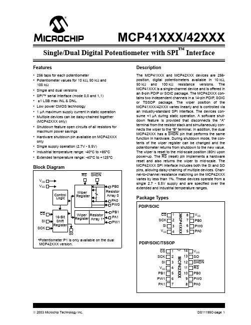
MCP41XXX/42XXX
1.0 ELECTRICAL CHARACTERISTICS DC CHARACTERISTICS: 10 kΩ VERSION
Electrical Characteristics: Unless otherwise indicated, VDD = +2.7V to 5.5V, TA = -40°C to +85°C (TSSOP devices are only specified at +25°C and +85°C). Typical specifications represent values for VDD = 5V, VSS = 0V, VB = 0V, TA = +25°C. Parameters Rheostat Mode Nominal Resistance Rheostat Differential Non Linearity Rheostat Integral Non Linearity Rheostat Tempco Wiper Resistance Wiper Current Nominal Resistance Match Potentiometer Divider Resolution Monotonicity Differential Non-Linearity Integral Non-Linearity Voltage Divider Tempco Full Scale Error Zero Scale Error Resistor Terminals Voltage Range Capacitance (CA or CB) Capacitance Bandwidth -3dB Settling Time Resistor Noise Voltage Crosstalk Schmitt Trigger High-Level Input Voltage Schmitt Trigger Low-Level Input Voltage Hysteresis of Schmitt Trigger Inputs Low-Level Output Voltage High-Level Output Voltage Input Leakage Current Pin Capacitance (All inputs/outputs) Power Requirements Operating Voltage Range Supply Current, Active Supply Current, Static Power Supply Sensitivity Note 1: 2: 3: 4: 5: 6: VDD IDDA IDDS PSS PSS 2.7 — — — — — 340 0.01 0.0015 0.0015 5.5 500 1 0.0035 0.0035 V µA µA %/% %/% VDD = 5.5V, CS = VSS, fSCK = 10 MHz, SO = Open, Code FFh (Note 6) CS, SHDN, RS = VDD = 5.5V, SO = Open (Note 6) VDD = 4.5V - 5.5V, VA = 4.5V, Code 80h VDD = 2.7V - 3.3V, VA = 2.7V, Code 80h CW BW tS eNWB CT VIH VIL VHYS VOL VOH ILI CIN, COUT VA,B,W 0 — — — — — — 0.7VDD — — — VDD - 0.5 -1 — — 15 5.6 1 2 9 -95 — — 0.05VDD — — — 10 VDD — — — — — — — 0.3VDD — 0.40 — +1 — V V µA pF IOL = 2.1 mA, VDD = 5V IOH = -400 µA, VDD = 5V CS = VDD, VIN = VSS or VDD, includes VA SHDN=0 VDD = 5.0V, TA = +25°C, fc = 1 MHz pF pF MHz µS nV/√Hz dB V V Note 4 f = 1 MHz, Code = 80h, see Figure 2-30 f = 1 MHz, Code = 80h, see Figure 2-30 VB = 0V, Measured at Code 80h, Output Load = 30 PF VA = VDD,VB = 0V, ±1% Error Band, Transition from Code 00h to Code 80h, Output Load = 30 pF VA = Open, Code 80h, f =1 kHz VA = VDD, VB = 0V (Note 5) N N DNL INL ∆VW/∆T VWFSE VWFSE VWZSE VWZSE 8 8 -1 -1 — -2 -2 0 0 — — ±1/4 ±1/4 1 -0.7 -0.7 +0.7 +0.7 — — +1 +1 — 0 0 +2 +2 Bits Bits LSB LSB LSB LSB LSB LSB Note 3 Note 3 Code FFh, VDD = 5V, see Figure 2-25 Code FFh, VDD = 3V, see Figure 2-25 Code 00h, VDD = 5V, see Figure 2-25 Code 00h, VDD = 3V, see Figure 2-25 R R-DNL R-INL ∆RAB/∆T RW RW IW ∆R/R 8 -1 -1 — — — -1 — 10 ±1/4 ±1/4 800 52 73 — 0.2 12 +1 +1 — 100 125 +1 1 kΩ LSB LSB ppm/°C Ω Ω mA % MCP42010 only, P0 to P1; TA = +25°C VDD = 5.5V, IW = 1 mA, code 00h VDD = 2.7V, IW = 1 mA, code 00h TA = +25°C (Note 1) Note 2 Note 2 Sym Min Typ Max Units Conditions
MAA50-2K481515SBP中文资料
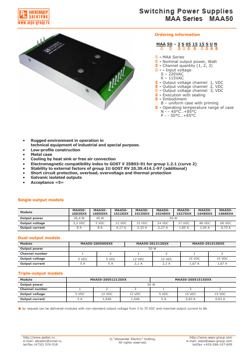
Switching on standart diagram
~In (L) ~In (N)
ground
FUin
~In (L) ~In (N)
+Out
Power module
Case
-Out
Сout1 Сout2
Rheat
FUin – current safety device 1A for input voltage 220VAC, 2A for input voltage 115VAC. Sout – ceramic condenser capacity 0,47-15 mcF with corresponding operating voltage to decrease high-frequency noise level. Sout2 – electronic condenser capacity 22-100 mcF in consideration with operating voltage and polarity. It makes for purpose to decrease
tel/fax +420-266-107-609
元器件交易网
Switching Power Supplies МАА Series MAA50
Output settings
№ pin Single-channel Dual-channel Triple-channel
1 case case case
Uout1 less than 20%
Output 2 and 3 multi-output execution (Inom 10 – 100%)
±13
Uout2&3 differs from
Z540中文资料(Intel)中文数据手册「EasyDatasheet - 矽搜」
Inte l proce ssor num be rs are not a m easure of pe rform ance . Proce ssor num be rs diffe re ntiate feature s within each proce ssor
Intel Virtualization Technology (Intel VT) requires a com puter system with an enabled Intel processor, BIO S, virtual m achine m onitor (VMM) and, for som e uses, certain platform software enabled for it. Functionality, perform ance or other benefits will vary depending on hardware and software configurations and m ay require a BIO S update. Software applications m ay not be com patible with all operating system s. Please check with your application vendor.
mcHF SDR QRP中文操作手册 V1.0 219.18
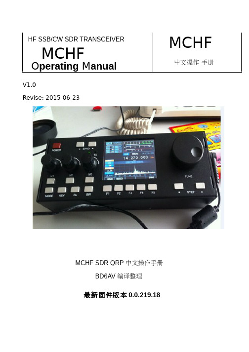
MCHF SDR QRP 中文操作手册
BD6AV 编译
2
整机设计指标参数:
基本参数: 频率范围: 发射: 工作模式: CW(A1A) AM(A3E) 最小频率步进: 天线阻抗: 工作温度范围: 频率稳定度: 工作电压: 工作电流: 50Ω -10℃---+60℃ ±1.5ppm @ 开机 5 分钟,-10℃~+60℃(标配) 9~15V DC 接收:410MA------440MA(最大显示亮度), 最小的LCD亮度可以降低40-60MA 硬件改进后降50%---80%,关机后约60MA 功放驱动级改进后3-5MA 发射:3A(FULL) 1.5A(5W) 整机尺寸: 发射机参数: 发射频段: 发射功率: 调制方式: 80,60,40,30,20,17,15,12和10米业余波段 标称5W(@13.8V),15W(@13.8V FULL) SSB 软件平衡调制 190x69x45 毫米 宽X高X厚 (不包括旋钮、ANT等突出突出物) 1Hz 接收: 2.5---30MH2–旋转编码器,M2 旋钮通常是用来调整射频增益 RFG 的,但其功能可以按 M2 键而改变,使用旋钮可调 整接收机 DSP 降噪器强度。在菜单模式,它是用来选择要调整的项目。而在正常(非菜单)状态下,按 M2 按键的时候,在接收模式时旋钮功能是调整 DSP 降噪器强度的。
MOOE 键
这个按键是用来选择收发信机的操作模式,按压这个按键将连续在 USB LSB CW-U AM 循环转换可用的模 式。但此按键在当菜单项“LSB / USB 汽车选择“启用,长按此键,将在普通转换模式和“LSB / USB 自动选择 “模式间转换,当“LSB / USB 自动选择“启用,它使电台根据频率自动选择 USB 或是 LSB(例如 USB 不会选 择低于 10 兆赫),如果要选择 CW 或是 AM 模式,长按 MOOE 键,回到普通模式,又可手动切换工作模式 了。
- 1、下载文档前请自行甄别文档内容的完整性,平台不提供额外的编辑、内容补充、找答案等附加服务。
- 2、"仅部分预览"的文档,不可在线预览部分如存在完整性等问题,可反馈申请退款(可完整预览的文档不适用该条件!)。
- 3、如文档侵犯您的权益,请联系客服反馈,我们会尽快为您处理(人工客服工作时间:9:00-18:30)。
OhmCraft’s revolutionary fine line, thick film technology, called FineFilm , provides an
entirely new level of stability and voltage ratings in chip resistors. Our MCH series of resistors meets the same high standards as our HVC series, but with the added feature of an extended temperature range.
♦Voltage Ratings to 40,000 Volts ♦Ohmic Values to 1,000 Gigohms ♦Ultra High Stability
♦Tight Tolerances ( to 0.1% ) ♦Low TCR and VCR ♦Very Low noise
♦
Extended Temperature Range
(-55ºC to +125ºC)
♦Custom Configurations
The usual hybrid technologies for manufacturing resistors depend upon composite materials that have limitations. Traditional thick-film methods severely limit
performance characteristics and thin-film methods are limited in attainable ohmic values. The FineFilm method of manufacturing offers the best characteristics of both methods, plus adds many unique features. FineFilm resistors feature a longer, high-aspect ratio trace of lower resistivity film. The combination of long line, high-aspect ratio, and higher conductivity film, give FineFilm
Note 1: Other standard & custom case sizes are available including: 0403, 0502, 0504, 1004, 1210 & 2510 Note 2: The continuous maximum voltage applied cannot exceed the maximum power rating.
MCH Series
Military Grade High Voltage Chip Resistors
Ratings
Case Size 1
0402 0503 0603 0805 1005 1206 1505 2010 2208 2512 3512 Max. Power (W) 0.040 0.050 0.060 0.200 0.250 0.330 0.330 1.000 0.750 2.000 3.000 Max. Voltage 2 (V)
(In air)
300 350 400 600 750 1000 1200 1700 2000 2500 3500 Max. Voltage (V) (Potted) 4000 6000 6000 10K 13K 16K 19K 30K 35K 40K 50K Resistance Range (ohms)
1K-20G
1K-200G
1K-300G
1K-350G
1K-450G
1K-500G
5K-750G
10K-1T
5K-1.5T
10K-2.0T
10K-2.0T
resistors unmatched design efficiency, versatility, linearity, stability and low noise. The FineFilm method allows control of process parameters to very tight tolerances. The result is chip resistors with outstanding stability and high voltage ratings.
Using the same method, a complete line of FineFilm leaded resistors, dividers and networks are manufactured. For information on those products, please refer to the appropriate data sheets.
L = Length W = Width T = Thickness D = Pad dimension
Dimensions
Wrap-around Type B & U terminations
Case Size
?
Length (L) (mils)
Width (W) (mils)
Thickness (T) Max. (mils)
Pad (D) (mils)
0402 40 + 5 20 + 3 20 10 (+ 5) 0403 40 + 5 30 + 5 20 10 (+ 5) 0502 50 (+10,-5) 25 + 5 20 10 (+ 5) 0503 55 (+10,-5) 30+ 5 20 6 (+ 2) 0504 50 (+10,-5) 40+ 5 20 6 (+ 2) 0603 63 (+10,-5) 31 + 5 20 10 (+10,-5) 0805
79 (+10,-5) 50 + 5 25 10 (+10,-5) 1004 100 (+10,-5) 40 + 5 25 15 (+10,-5) 1005 100 (+10,-5) 50 + 5 25 15 (+10,-5) 1206 126 (+10,-5) 63 + 5 30 15 (+10,-5) 1210 126 (+10,-5) 98 + 5 30 15 (+10,-5) 1505 150 (+10,-5) 50 + 5 30 15 (+10,-5) 2010 200 (+10,-5) 100 + 5 30 20 (+10,-5) 2208 225 (+10,-5) 75 + 5 30 20(+10,-5) 2510 250 (+10,-5) 100 + 5 30 20 (+10,-5) 2512 250 (+10,-5) 125 + 5 30 20 (+10,-5) 3512
350 (+10,-5)
125 + 5
30
20 (+10,-5)
Bondable Type G & S terminations。