1N3689B中文资料
1N系列二极管
250μ 250μ 250μ
250μ 250μ
250μ 250μ 250μ
250μ 250μ
250μ 250μ 250μ
250μ 250μ
250μ 250μ 250μ
250μ
400m
6.4
2m
400m
6.4
4m
400m
6.4
4m
400m
4m
400m
4m
400m
6.4 6.4 6.4 1N4612
4m
400m
4m
400m
4m
400m
6.4 6.4 6.4 1N4612A
4m
400m
6.4
4m
400m
6.4
4m
400m
6.4
1N4583-
1(A1)
Si 30 稳压
1N4583B Si 7 稳压
)
Si 7
稳压 稳压
1N4616DUR1 Si
1N4617(-1) Si 7
1N4617C(C1
)
Si 7
稳压 稳压
稳压
1N4617CUR1 Si
1N4617D(D1
)
Si 7
稳压 稳压
1N4617DUR1 Si
1N4618(-1) Si 7
1N4618C(C1
)
Si 7
稳压 稳压
稳压
4m 4m 4m
3.6 3.6
3.6 3.6 3.9 MZ4622
3.9 3.9
3.9 3.9 4.3 MZ4623
1N5519B中文资料

B-C-D SUFFIX MAX. NOISE DENSITY @1Z=250µ A ND
REGULATION FACTOR ∆VZ (NOTE 5) VOLTS
LOW VZ CURRENT 1ZL
mAdc
µ Adc
5.0 3.0 1.0 3.0 2.0 2.0 2.0 1.0 1.0 0.5 0.5 0.1 0.05 0.05 0.05 0.01 0.01 0.01 0.01 0.01 0.01 0.01 0.01 0.01 0.01 0.01 0.01 0.01 0.01
NOTE 2 NOTE 3 NOTE 4 NOTE 5
Reverse leakage currents are measured at VR as shown on the table. ∆VZ is the maximum difference between VZ at lZT and VZ at lZL measured with the device junction in thermal equilibrium at the ambient temperature of +25°C +3°C.
Junction and Storage Temperature: -65°C to +175°C DC Power Dissipation: 500 mW @ +50°C Power Derating: 4 mW / °C above +50°C Forward Voltage @ 200mA: 1.1 volts maximum ELECTRICAL CHARACTERISTICS @ 25°C
26 24 22 18 22 26 30 30 30 35 40 45 60 80 90 90 100 100 100 100 100 100 100 100 100 100 100 100 100
1N4749中文资料
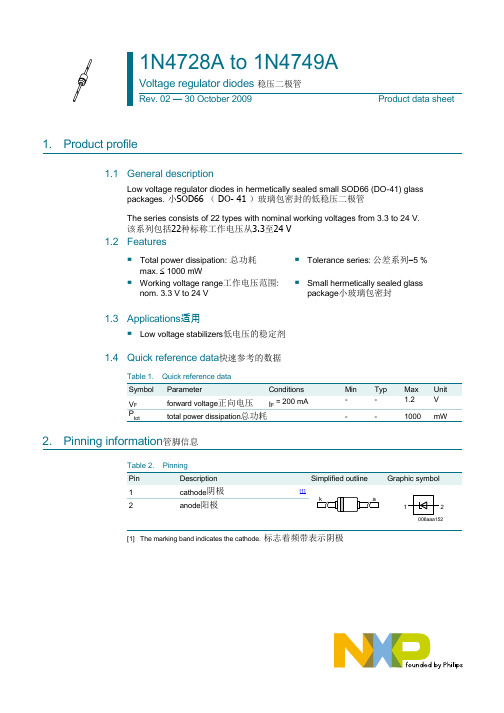
1N4728A to 1N4749AVoltage regulator diodes 稳压二极管Rev. 02 — 30 October 2009 Product data sheet1. Product profile1.1 General descriptionLow voltage regulator diodes in hermetically sealed small SOD66 (DO-41) glasspackages.小SOD66 ( DO- 41 )玻璃包密封的低稳压二极管The series consists of 22 types with nominal working voltages from 3.3 to 24 V.该系列包括22种标称工作电压从3.3至24 V1.2 Features■ Total power dissipation:总功耗■ Tolerance series: 公差系列-5 %max. ≤ 1000 mW■ Working voltage range工作电压范围: ■ Small hermetically sealed glassnom. 3.3 V to 24 V package小玻璃包密封1.3 Applications适用■ Low voltage stabilizers低电压的稳定剂1.4 Quick reference data快速参考的数据V F forward voltage正向电压I FPtotal power dissipation总功耗- - 1000 mW tot2. Pinning information管脚信息1 cathode[1]2 anode阳极 1 2006aaa152[1] The marking band indicates the cathode.标志着频带表示阴极Voltage regulator diodes3. Ordering informationTable 3. Ordering information1N4749A[1]2 leads[1] The series consists of 22 types with nominal working voltages from 3.3 V to 24 V.4. MarkingTable 4. Marking codes5. Limiting values 极限值Table 5. Limiting valuesIn accordance with the Absolute Maximum Rating System (IEC 60134). 按照绝对最大额定值系统I F forward current - 500 mAI Z working current 工作电流- see Table 8 I ZSM non-repetitive peak reverse- see current 非重复性反向电流峰值Table 8 P tot total power dissipation 总功耗 T amb = 50︒C - 1000 mW T jjunction temperature 结温 -65 +200 ︒C T stgstorage temperature 存储温度-65+200︒CVoltage regulator diodes6. Thermal characteristics 热特性Table 6. Thermal characteristics 热特性 th(j-t)junction to tie-point 配合点结的热电阻7. Characteristics 特征Table 7. CharacteristicsT j = 25 ︒C unless otherwise specified. V Fforward voltage 正向电压I FVoltage regulator diodes Table 8. Characteristics per type每种型号的特征T j = 25 ︒C unless otherwise specified.型号工作电压测试电流电阻差反向电流工作电流非重复性反向峰值电流1N4729A 3.6 69 10 400 1 100 1 252 12601N4730A 3.9 64 9 400 1 50 1 234 11901N4731A 4.3 58 9 400 1 10 1 217 10701N4732A 4.7 53 8 500 1 10 1 193 9701N4733A 5.1 49 7 550 1 10 1 178 8901N4734A 5.6 45 5 600 1 10 2 162 8101N4735A 6.2 41 2 700 1 10 3 146 7301N4736A 6.8 37 3.5 700 1 10 4 133 6601N4737A 7.5 34 4 700 0.5 10 5 121 6051N4738A 8.2 31 4.5 700 0.5 10 6 110 5501N4739A 9.1 28 5 700 0.5 10 7 100 5001N4740A 10 25 7 700 0.25 10 7.6 91 4541N4741A 11 23 8 700 0.25 5 8.4 83 4141N4742A 12 21 9 700 0.25 5 9.1 76 3801N4743A 13 19 10 700 0.25 5 9.9 69 3441N4744A 15 17 14 700 0.25 5 11.4 61 3041N4745A 16 15.5 16 700 0.25 5 12.2 57 2851N4746A 18 14 20 750 0.25 5 13.7 50 2501N4747A 20 12.5 22 750 0.25 5 15.2 45 2251N4748A 22 11.5 23 750 0.25 5 16.7 41 2051N4749A 24 10.5 25 750 0.25 5 18.2 38 190[1] V Z is measured with device at thermal equilibrium while held in clips at 10 mm from body in still air at 25 ︒C.[2] Half square wave or equivalent sine wave pulse 1/120 second duration superimposed on I test.Voltage regulator diodes300I F(mA)2001000 0.5mbg925 (1) (2)V F (V) 1.0(1) T j = 200 ︒C(2) T j = 25 ︒CFig 2. Forward current as a function of forward voltage; typical values正向电流-正向电压函数Voltage regulator diodes 8. Package outline 包装外形Hermetically sealed glass package; axial leaded; 2 leads密封玻璃封装;轴向引脚; 2引脚SOD66Fig 3. Package outline SOD66 (DO-41)Voltage regulator diodes 9. Packing information 包装信息Table 9. Packing methodsThe indicated -xxx are the last three digits of the 12NC ordering code.[1]1N4749A[2] 52 mm reel pack, axial -113[1] For further information and the availability of packing methods, see Section 11.[2] The series consists of 22 types with nominal working voltages from 3.3 V to 24 V.Voltage regulator diodes 10. Revision historyTable 10. Revision historyModifications: • The format of this data sheet has been redesigned to comply with the new identityguidelines of NXP Semiconductors.• Legal texts have been adapted to the new company name where appropriate.•Table 5 “Limiting values”: I ZM redefined to I Z working current• Table 6: R th(j-tp) redefined to R th(j-t) thermal resistance from junction to tie-point• Figure 1: R th(j-tp) redefined to R th(j-t) thermal resistance from junction to tie-point•Table 8 “Characteristics per type”: I Ztest redefined to I test test current•Figure 3 “Package outline SOD66 (DO-41)”: updated1N4728A_1 19960426 Product data sheet - -Voltage regulator diodes11. Legal information11.1 Data sheet statusPreliminary [short] data sheet Qualification This document contains data from the preliminary specification. Product [short] data sheet ProductionThis document contains the product specification.[1] Please consult the most recently issued document before initiating or completing a design. [2] The term …short data sheet‟ is explained in section “Definitions”.[3]The product status of device(s) described in this document may have changed since this document was published and may differ in case of multiple devices. The latest product status information is available on the Internet at URL .11.2 DefinitionsDraft — The document is a draft version only. The content is still under internal review and subject to formal approval, which may result in modifications or additions. NXP Semiconductors does not give any representations or warranties as to the accuracy or completeness ofinformation included herein and shall have no liability for the consequences of use of such information.Short data sheet — A short data sheet is an extract from a full data sheet with the same product type number(s) and title. A short data sheet is intended for quick reference only and should not be relied upon to contain detailed and full information. For detailed and full information see the relevant full data sheet, which is available on request via the local NXP Semiconductors sales office. In case of any inconsistency or conflict with the short data sheet, the full data sheet shall prevail.11.3 DisclaimersGeneral — Information in this document is believed to be accurate andreliable. However, NXP Semiconductors does not give any representations or warranties, expressed or implied, as to the accuracy or completeness of such information and shall have no liability for the consequences of use of such information.Right to make changes — NXP Semiconductors reserves the right to make changes to information published in this document, including withoutlimitation specifications and product descriptions, at any time and without notice. This document supersedes and replaces all information supplied prior to the publication hereof.Suitability for use — NXP Semiconductors products are not designed, authorized or warranted to be suitable for use in medical, military, aircraft, space or life support equipment, nor in applications where failure ormalfunction of an NXP Semiconductors product can reasonably be expected to result in personal injury, death or severe property or environmental12. Contact informationdamage. NXP Semiconductors accepts no liability for inclusion and/or use of NXP Semiconductors products in such equipment or applications and therefore such inclusion and/or use is at the customer‟s own risk.Applications — Applications that are described herein for any of these products are for illustrative purposes only. NXP Semiconductors makes no representation or warranty that such applications will be suitable for the specified use without further testing or modification.Limiting values — Stress above one or more limiting values (as defined in the Absolute Maximum Ratings System of IEC 60134) may cause permanent damage to the device. Limiting values are stress ratings only and operation of the device at these or any other conditions above those given in theCharacteristics sections of this document is not implied. Exposure to limiting values for extended periods may affect device reliability.Terms and conditions of sale — NXP Semiconductors products are sold subject to the general terms and conditions of commercial sale, as published at /profile/terms , including those pertaining to warranty, intellectual property rights infringement and limitation of liability, unlessexplicitly otherwise agreed to in writing by NXP Semiconductors. In case of any inconsistency or conflict between information in this document and such terms and conditions, the latter will prevail.No offer to sell or license — Nothing in this document may be interpreted or construed as an offer to sell products that is open for acceptance or the grant, conveyance or implication of any license under any copyrights, patents or other industrial or intellectual property rights.Export control — This document as well as the item(s) described herein may be subject to export control regulations. Export might require a prior authorization from national authorities.Quick reference data — The Quick reference data is an extract of the product data given in the Limiting values and Characteristics sections of this document, and as such is not complete, exhaustive or legally binding.11.4 TrademarksNotice: All referenced brands, product names, service names and trademarks are the property of their respective owners.For more information, please visit: For sales office addresses, please send an email to: salesaddresses@Voltage regulator diodes 13. Contents1 Product profile . . . 11.1 General description. . . 11.2 Features . . . 11.3 Applications . . . 11.4 Quick reference data. . . 12 Pinning information . . . 13 Ordering information . . . 24 Marking . . . 25 Limiting values . . . 26 Thermal characteristics. . . 37 Characteristics . . . 38 Package outline . . . 69 Packing information. . . 710 Revision history . . . 811 Legal information . . . 911.1 Data sheet status . . . 911.2 Definitions . . . 911.3 Disclaimers . . . 911.4 Trademarks . . . 912 Contact information . . . 913 Contents . . . 10Please be aware that important notices concerning this document and the product(s)described herein, have been included in section …Legal information‟.© NXP B.V. 2009. All rights reserved.For more information, please visit: For sales office addresses, please send an email to: salesaddresses@Mouser ElectronicsAuthorized DistributorClick to View Pricing, Inventory, Delivery & Lifecycle Information:NXP:1N4728A,113 1N4729A,113 1N4730A,113 1N4731A,113 1N4732A,113 1N4733A,113 1N4734A,1131N4735A,113 1N4736A,113 1N4737A,113 1N4738A,113 1N4739A,113 1N4740A,113 1N4741A,113 1N4742A,113 1N4743A,113 1N4744A,113 1N4745A,113 1N4746A,113 1N4747A,113 1N4748A,113 1N4749A,1131N4728A,133 1N4729A,133 1N4730A,133 1N4731A,133 1N4732A,133 1N4733A,133 1N4734A,133 1N4735A,133 1N4736A,133 1N4737A,133 1N4738A,133 1N4739A,133 1N4740A,133 1N4741A,133 1N4742A,1331N4743A,133 1N4744A,133 1N4745A,133 1N4746A,133 1N4747A,133 1N4748A,133 1N4749A,133。
SSU1N60B中文资料

SSR1N60B / SSU1N60B
November 2001
SSR1N60B / SSU1N60B
600V N-Channel MOSFET
General Description
These N-Channel enhancement mode power field effect transistors are produced using Fairchild’s proprietary, planar, DMOS technology. This advanced technology has been especially tailored to minimize on-state resistance, provide superior switching performance, and withstand high energy pulse in the avalanche and commutation mode. These devices are well suited for high efficiency switch mode power supplies.
BVDSS ∆BVDSS / ∆TJ
Drain-Source Breakdown Voltage
Breakdown Voltage Temperature Coefficient
VGS = 0 V, ID = 250 µA
600 --
ID = 250 µA, Referenced to 25°C -- 0.65
-- 5.9
VGS = 10 V
-- 1.0
(Note 4, 5) --
2.7
--10 100 100 -100
DS1856B-020R中文资料
Operating Temperature Range ...........................-40°C to +95°C Programming Temperature Range .........................0°C to +70°C Storage Temperature Range .............................-55°C to +125°C Soldering Temperature .......................................See IPC/JEDEC J-STD-020A
1
For pricing delivery, and ordering information please contact Maxim/Dallas Direct! at 1-888-629-4642, or visit Maxim’s website at .
元器件交易网
Pin Configurations
TOP VIEW A SDA 1 IN1 SCL VCC H1 SCL 2 OUT1 3 L1 IN1 4 16 VCC 15 H1 14 L1
TO LASER BIAS CONTROL TO LASER MODULATION CONTROL
DS1856
L0
B
OUT2
Stresses beyond those listed under “Absolute Maximum Ratings” may cause permanent damage to the device. These are stress ratings only, and functional operation of the device at these or any other conditions beyond those indicated in the operational sections of the specifications is not implied. Exposure to absolute maximum rating conditions for extended periods may affect device reliability.
1N5391-1N5399中文资料,PDF资料
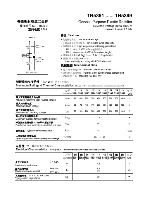
1N 53921N 53931N 53941N 53951N 53961N 53971N 53988001002003004005006001002003004005006008007014028035042056045501.51.2V 5.0200μA pFI R1N5391 ...... 1N53991N 5399100010007001N 5391505035201N 53921N 53931N 53941N 53951N 53961N 53971N 53981N53991N 5391普通塑封整流二极管反向电压 50 ---1000 V正向电流 1.5 AGeneral Purpose Plastic RectifierReverse Voltage 50 to 1000 VForward Current 1.5A210Cj最大正向电压 I F = 1.5A 最大反向电流 TA= 25℃典型结电容 V R = 4.0V, f = 1MHz TA=100℃ Maximum forward voltageMaximum reverse current Type junction capacitanceVF符号Symbols 单位Unit电特性 TA = 25℃ 除非另有规定。
Electrical Characteristics Ratings at 25℃ ambient temperature unless otherwise specified.最大可重复峰值反向电压Maximum repetitive peak reverse voltage 最大均方根电压 Maximum RMS voltage 最大直流阻断电压Maximum DC blocking voltage最大正向平均整流电流Maximum average forward rectified current 峰值正向浪涌电流 8.3ms单一正弦半波Peak forward surge current 8.3 ms single half sine-wave典型热阻 Typical thermal resistance工作结温和存储温度Operating junction and storage temperature range-55 --- +150 V V V A A℃/WV RRM V RMS V DC I F(AV)I FSM ℃Tj, TSTG极限值和温度特性 TA = 25℃ 除非另有规定。
1N1N8G中文资料
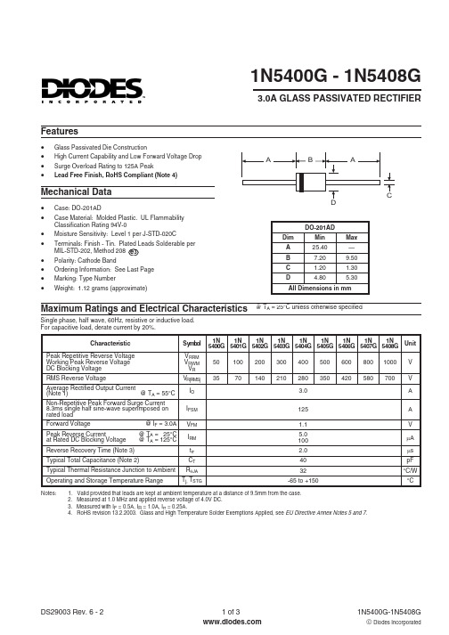
e 31N5400G - 1N5408G3.0A GLASS PASSIVATED RECTIFIERFeaturesMaximum Ratings and Electrical Characteristics@ T A = 25°C unless otherwise specified·Glass Passivated Die Construction·High Current Capability and Low Forward Voltage Drop ·Surge Overload Rating to 125A Peak ·Lead Free Finish,RoHS Compliant (Note 4)Mechanical Data·Case: DO-201AD·Case Material: Molded Plastic. UL Flammability Classification Rating 94V-0·Moisture Sensitivity: Level 1 per J-STD-020C ·Terminals: Finish - Tin. Plated Leads Solderable per MIL-STD-202, Method 208·Polarity: Cathode Band·Ordering Information: See Last Page ·Marking: Type Number·Weight: 1.12 grams (approximate)Single phase, half wave, 60Hz, resistive or inductive load.For capacitive load, derate current by 20%.Notes:1. Valid provided that leads are kept at ambient temperature at a distance of 9.5mm from the case.2. Measured at 1.0 MHz and applied reverse voltage of 4.0V DC.3. Measured with I F = 0.5A, I R = 1.0A,I rr = 0.25A.4.RoHS revision 13.2.2003. Glass and High Temperature Solder Exemptions Applied, see EU Directive Annex Notes 5 and 7.I ,I N S T A N T A N E O U S F O R W A R D C U R R E N T (A )F V ,INSTANTANEOUS FORWARD VOLTAGE (V)Fig.2Typical Forward CharacteristicsF 0.010.11.0101000.40.60.81.01.21.41.61.810100200110100I ,P E A K F O R W A R D S U R G E C U R R E N T (A )F S M NUMBER OF CYCLES AT 60Hz Fig.3Peak Forward SurgeCurrent10100200110100C ,T O T A L C A P A C I T A N C E (p F )T V ,REVERSE VOLTAGE (V)Fig.4Typical Total CapacitanceR 0.11.01010020406080100120140PERCENT OF RATED PEAK VOLTAGE (%)Fig.5Typical Reverse Characteristics012340255075100125150175I ,A V E R A G E F O R W A R D R E C T I F I E D C U R R E N T (A )O T ,AMBIENTTEMPERATURE (°C)Fig.1Forward Current Derating CurveAOrdering Information(Note 5)Notes: 5. For packaging details, visit our website at /datasheets/ap02008.pdfIMPORTANT NOTICEDiodes Incorporated and its subsidiaries reserve the right to make modifications,enhancements,improvements,corrections or other changes without further notice to any product herein.Diodes Incorporated does not assume any liability arising out of the application or use of any product described herein;neither does it convey any license under its patent rights,nor the rights of others.The user of products in such applications shall assume all risks of such use and will agree to hold Diodes Incorporated and all the companies whose products are represented on our website,harmless against all damages.LIFE SUPPORTDiodes Incorporated products are not authorized for use as critical components in life support devices or systems without the expressed written approval of the President of Diodes Incorporated.。
1N829中文资料

Philips Semiconductors
Product specification
Voltage reference diodes
PACKAGE OUTLINE
1N821 to 1N829 1N821A to 1N829A
handbook, full pagewidth
0.55 max 1.6 max 25.4 min 3.04 max 25.4 min
1996 Mar 20
2Hale Waihona Puke 元器件交易网Philips Semiconductors
Product specification
Voltage reference diodes
ELECTRICAL CHARACTERISTICS Tj = 25 °C unless otherwise specified. SYMBOL Vref ∆Vref PARAMETER reference voltage reference voltage excursion 1N821; 1N821A 1N823; 1N823A 1N825; 1N825A 1N827; 1N827A 1N829; 1N829A SZ temperature coefficient 1N821; 1N821A 1N823; 1N823A 1N825; 1N825A 1N827; 1N827A 1N829; 1N829A rdif differential resistance 1N821 to 1N829 1N821A to 1N829A Notes IZ = 7.5 mA; see Fig.4 − − IZ = 7.5 mA: see Fig.3; notes 1 and 2 CONDITIONS IZ =7.5 mA IZ =7.5 mA; test points for Tamb: −55; +25; +75; +100 °C; see Fig.2; notes 1 and 2 MIN. 5.89 − − − − − − − − − −