101_Utility_and_Substation_Testing_AG
PFSWITCH 2048T 商品说明书
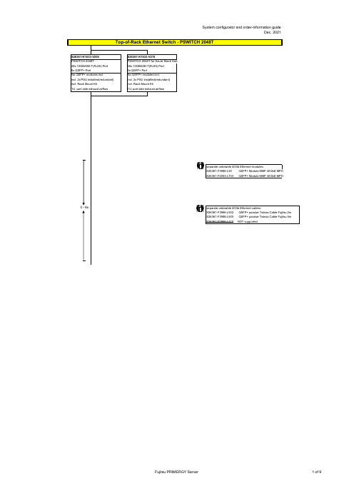
no power cord
T26139-Y3850-E10
T26139-Y1968-L180 T26139-Y1968-L250 T26139-Y1968-L10
T26139-Y1741-L90
T26139-Y1757-L10 T26139-Y1753-L10 T26139-Y1740-L10 T26139-Y1744-L10 T26139-Y1745-L10 T26139-Y1746-L10 T26139-Y1747-L18 T26139-Y1748-L10
Region Kits, 1x per System Region Kit Europe, Contains warranty sheet and safety instructions in German, English, French, Spanish, Italian, Polish, Russian and Welsh language
S26361-F1452-E100 S26361-F1452-E130
End of PSWITCH 2048T
CAT 6A S/STP RJ45 cables can be used for proper cabling: S26361-F3417-L602: CAT 6A, RJ45 connector, 2m S26361-F3417-L603: CAT 6A, RJ45 connector, 3m S26361-F3417-L605: CAT 6A, RJ45 connector, 5m S26361-F3417-L610: CAT 6A, RJ45 connector, 10m S26361-F3417-L615: CAT 6A, RJ45 connector, 15m
IC+最新85NM工艺的PHY IP101G_DS_R01_20121224
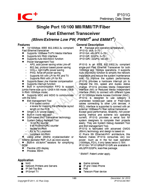
Single Port 10/100 MII/RMII/TP/FiberFast Ethernet Transceiver(85nm/Extreme Low PW, PWMT ® and EMIMT ®)Features General DescriptionIP1IP1IP1IP1z 10/100Mbps IEEE 802.3/802.3u compliant Fast Ethernet transceiverz Supports 100Base-TX/FX Media Interface z Supports MII/ RMII Interfacez Supports Auto MDI/MDIX function z Power Management Tool- APS, auto power saving while Link-off - 802.3az, protocol based power saving - WOL+, light traffic power saving - PWD, force-off power saving- Supports MII with LPI for RX and TX - Supports RMII with LPI for RXz Supports Base Line Wander compensation z Supports Interrupt functionz Built in synchronization FIFO to support jumbo frame size up to 12KB in MII mode (10KB in RMII 100Mbps mode)z Supports MDC and MDIO to communicate with the MACz EMI Management Tool - F/W based control- 4 levels for mapping the difference layoutlength on the PCBz Single 3.3V power supply z Built-in Vcore regulatorz DSP-based PHY Transceiver technology z System Debug Assistant Tool - 16 bit RX counter- 9 bit RXError/CRC counter - Isolate MII/RMII - RX to TX Loopback - Loopback MII/RMIIz Using either 25MHz crystal/oscillator or 50MHz oscillator REF_CLK as clock sourcez Built-in 49.9ohm resistors for simplifying BOMz Flexible LED display z Process: 85nmz Package and operation temperature 01G: dice, 0~70℃01GA: 48LQFP , 0~70℃ 01GR: 32QFN, 0~70℃ 01GRI: 32QFN, -40~85℃IP101G is an IEEE 802.3/802.3u compliant single-port Fast Ethernet Transceiver for both 100Mbps and 10Mbps operations. It supports Auto MDI/MDIX function to simplify the network installation and reduce the system maintenance cost. To improve the system performance, IP101G provides a hardware interrupt pin to indicate the link, speed and duplex status change. IP101G provides Media Independent Interface (MII) or Reduced Media Independent Interface (RMII) to connect with different types of 10/100Mbps Media Access Controller (MAC). IP101G is designed to use category 5 unshielded twisted-pair cable or Fiber-Optic cables connecting to other LAN devices. A PECL interface is supported to connect with an external 100Base-FX fiber optical transceiver. Except good performance, reliability, rich power saving method and extreme low operating current, IP101G provides a serial tool for system designers to complete their projects easily. They are System Debug Assistant Tool and EMI Management Tool.IP101G is fabricated with advanced CMOS (85nm) technology and design is based onIC Plus’s 5th Ethernet-PHY architecture, this feature makes IP101G consumes very low power. Such as in the full load operation (100Mbps_FDX), it only takes below 0.15W. IP101GA / IP101GR&IP101GRI are available in 48LQFP/32QFN, lead-free package.* EMIMT: Patent under apply.Application■ NAS■ Network Printers and Servers ■ IP Set-Top Box ■IP/Smart TV■ Game console■ IP and Video Phone ■ PoE■Telecom Fiber deviceTable Of ContentsTable Of Contents (2)List of Figures (4)List of Tables (5)Revision History (6)Features comparison between IP101G and IP101A/IP101AH (7)Transmit and Receive Data Path Block Diagram (8)1Pin diagram (9)2Dice pad information (11)3Pin description (12)3.1IP101GA pin description (12)3.2IP101GR/GRI pin description (16)4Register Descriptions (19)4.1Register Page mode Control Register (20)4.2MII Registers (20)4.3MMD Control Register (30)4.4MMD Data Register (31)4.5RX Counter Register (34)4.6LED Mode Control Register (35)4.7WOL+ Control Register (35)4.8UTP PHY Specific Control Register (38)4.9Digital IO Pin Control Register (39)5Function Description (41)5.1Major Functional Block Description (41)5.1.1Transmission Description (41)5.1.2MII and Management Control Interface (42)5.1.3RMII Interface (43)5.1.4Flexible Clock Source (45)5.1.5Auto-Negotiation and Related Information (45)5.1.6Auto-MDIX function (46)5.2PHY Address Configuration (46)5.3Power Management Tool (47)5.3.1Auto Power Saving Mode (47)5.3.2IEEE802.3az EEE (Energy Efficient Ethernet) (48)5.3.3Force power down (48)5.3.4WOL+ operation mode (48)5.4LED Mode Configuration (52)5.5LED Blink Timing (52)5.6Repeater Mode (52)5.7Interrupt (52)5.8Miscellaneous (52)5.9Serial Management Interface (53)5.10Fiber Mode Setting (54)5.11Jumbo Frame (54)6Layout Guideline (55)6.1General Layout Guideline (55)6.2Twisted Pair recommendation (55)7Electrical Characteristics (56)7.1Absolute Maximum Rating (56)7.2DC Characteristics (56)7.3Crystal Specifications (57)7.4AC Timing (58)7.4.1Reset, Pin Latched-in, Clock and Power Source (58)7.4.2MII Timing (59)7.4.3RMII Timing (60)7.4.4SMI Timing (61)7.5Thermal Data (61)8Order Information (62)9Physical Dimensions (63)9.148-PIN LQFP (63)9.232-PIN QFN (64)List of FiguresFigure 1 Flow chart of IP101G (8)Figure 2 IP101GA 48 Pin Diagram (9)Figure 3 IP101GR/GRI 32 Pin Diagram (10)Figure 4 IP101G dice pad information (11)Figure 5 LPI transition (43)Figure 6 IP101G/GA/GR/GRI MII Mode with LPI transition Block Diagram (43)Figure 7 IP101G/GA/GR/GRI MII Mode without LPI transition Block Diagram (43)Figure 8 IP101G RMII Mode with internal clock Block Diagram (44)Figure 9 IP101G RMII Mode with external clock Block Diagram (44)Figure 10 IP101G RMII Clock Application Circuit (45)Figure 11 IP101G link speed and EEE ability programming guide (46)Figure 12 PHY Address Configuration (47)Figure 13 Magic Packet Format (49)Figure 14 Sleep or wake up automatically programming guide (50)Figure 15 MAC control sleep or wake up programming guide (51)Figure 16 MDC/MDIO Format (53)Figure 17 IP101G Fiber Mode Setting (54)Figure 18 Reset, Pin Latched-In, Clock and Power Source Timing Requirements (58)Figure 19 MII Transmit Timing Requirements (59)Figure 20 MII Receive Timing Specifications (59)Figure 21 RMII Transmit Timing Requirements (60)Figure 22 RMII Receive Timing Specifications (60)Figure 23 SMI Timing Requirements (61)Figure 24 48-PIN LQFP Dimension (63)Figure 25 32-PIN QFN Dimension (64)List of TablesTable 1 Features comparison between IP101G and IP101A/IP101AH (7)Table 2 Register Map (19)Table 3 Flexible Clock Source Setting (45)Table 4 PHY Address Configuration (47)Table 5 WOL+ operation mode (49)Table 6 LED Mode 1 Function (52)Table 7 LED Mode 2 Function (52)Table 8 LED Blink Timing (52)Table 9 SMI Format (53)Table 10 DC Characteristics (56)Table 11 I/O Electrical Characteristics (56)Table 12 Pin Latched-in Configuration Resistor (57)Table 13 Crystal Specifications (57)Table 14 Reset, Pin Latched-in, Clock and Power Source Timing Requirements (58)Table 15 MII Transmit Timing Requirements (59)Table 16 MII Receive Timing Specifications (59)Table 17 RMII Transmit Timing Requirements (60)Table 18 RMII Receive Timing Specifications (60)Table 19 SMI Timing Requirements (61)Table 20 Thermal Data (61)Table 21 Part Number and Package (62)Revision HistoryRevision # Change DescriptionIP101G-DS-R01 Initial release.IP101G-DS-R01-20120522 1) Correct the typo of Digital IO Pin Control Register.2) Modify the operation voltage REGOUT and DVDD_REGIN of DCCharacteristics.IP101G-DS-R01-20120611 1) Correct the typo of Linear Regulator Output Control Register.2) Correct the typo of pin description for pin type PD and PU.3) Modify the register description for RMII_V12 and RMII_V10.4) Correct the typo of register default values.5) Modify the operation voltage DVDD33_IO of DC Characteristics.IP101G-DS-R01-20120622 Add 30 seconds into the definition for register WOL_PLUS_TIMER_SEL.IP101G-DS-R01-20120629 Add the symbol SC (Self Clear) for PHY MII register 0.15 Reset and 0.9Restart Auto-Negotiation.IP101G-DS-R01-20120709 1) Add LED mode 2 in the pin description and function description.2) Correct the table of LED Blink Timing.3) Add more description of PHY Address Configuration and IEEE 802.3az.4) Add ESD reliability of Absolute Maximum Rating.5) Correct the typo of function description for Auto Power Saving Mode.6) Change register P16R16[10] description from HEART_BEAT_EN toReserved.IP101G-DS-R01-20120719 Correct the table of Register Map for page selection.IP101G-DS-R01-20120726 1) Add more description of Register RX2TX_LPBK P1R23[13] for Rx to Txloopback test.2) Add more description on Fiber Mode Setting and latched-in pin signalson AC Timing.3) Add IP101AH into the table of features comparison.IP101G-DS-R01-20120808 1) Correct the I/O type of IP101GA pin description to O(Ouput) for pin24RXER.2) Change the pin name from DVDD33_IO to VDDIO.IP101G-DS-R01-20120821 1) Change the default value of register P16R27 from 0x0022 to 0x0012.2) Remove I/O Slew Rate Control Register.3) Change the register location RMII_WITH_ER from P16R29[0] toP16R29[7].IP101G-DS-R01-20120927 1) Add more description of low power idle (LPI) state in MII and RMIImodes.2) Correct the typo of Physical Dimensions.IP101G-DS-R01-20121101 Change the LED blink timing from “On 80ms -> Off (20~40)ms” to “On 26ms-> Off 78ms”.IP101G-DS-R01-20121113 Add more function description to support Jumbo Frame.IP101G-DS-R01-20121127 Change the LED mode function as same as IP101A.IP101G-DS-R01-20121224 Add the notice that does not let these PHY address pins floating for thelatched-in settings after the power is ready.DisclaimerThis document probably contains the inaccurate data or typographic error. In order to keep this document correct, IC Plus reserves the right to change or improve the content of this document.Features comparison between IP101G and IP101A/IP101AHTable 1 Features comparison between IP101G and IP101A/IP101AHProduct Name IP101GR IP101G IP101GA IP101A IP101AH Package Type 32pin QFN Dice 48pin LQFP48pin LQFPREGOUT(1) Output Voltage and location 1.0V, pin28 1.0V, pad5and pad111.0V, pin82.5V, pin32REGIN Input Voltage and location NA(2) 1.0V, pad23and pad26NA 2.5V, pin8RMII mode setting Pin4 Pad18 Pin1 Pin1 and pin44Fiber mode setting: Fiber FXSD signal: Pin19Pin1Pad39Pad13Pin22Pin43NA Pin24 and pin48Pin37Number of LED 2 4 4 5LED mode 1 and 2 1 and 2LED Blink Timing On 26ms -> Off 78ms On 26ms -> Off 78msPHY address number(3) Single: 0 ~ 1Multi: 2 ~ 31Single: 0 ~ 7Multi: 8 ~ 31Single: 0 ~ 31Center-tap of transformer Do not connect to any power 2.5V input power Built-in 49.9ohm resistors Yes No Power consumption ~150mW ~480mW Process 85nm 0.25μm IEEE 802.3az Yes No10Base TX amplitude ~1.75V (10Base-Te) ~2.5V (10Base-T) WOL+ (Wake On LAN Plus) Yes NoAnalog OFF Yes No16 bit RX counter Yes No9 bit RXER/CRC counter Yes NoRX to TX Loopback Yes No Loopback MII/RMII Yes YesSNI mode No Yes Note 1: Regulator voltage output is for internal use only. Do not supply to any other device.Note 2: Not available for this function. The 1.0V is supplied by the regulator that built-in the chip.Note 3: Do not let these PHY address pins floating for the latched-in settings after the power is ready.Transmit and Receive Data Path Block DiagramFigure 1 Flow chart of IP101G1Pin diagramRXER CRS/LEDMODRXDV/CRS_DV/FX_HEN X1X2RXD2RXD3RXCLK/50M_CLKO DGNDRXD0NCRESET_N IP101GA (LQFP-48)242322212019181716NC NC TXER/FXSDNC Note:Those pins in "blue "are different from IP101A.NC RXD1INTRNC DGNDNC LED3/PHY_AD3VDDIOFigure 2 IP101GA 48 Pin DiagramIP101GR/GRI(VQFN-32)(GND on bottom of chip)RXD3TXCLK/50M_CLKI RXCLK/50M_CLKO LED0/PHY_AD0LED3/PHY_AD3161514131211109RESET_NISET REGOUT MDI_TN MDI_TP MDI_RP MDI_RN RXD2AVDD33Figure 3 IP101GR/GRI 32 Pin Diagram2Dice pad informationIC LogoPad 1Pad 44Pad 11Pad 45Pad 24Pad 31Pad 12Pad 22Pad 23REGINPHYAD_LED028PHYAD_LED129VSS30PHYAD_LED231PHYAD_LED332VDDIO 33RX_CLK REGOUT 34VSSIO RESET_N 35RXD[3]TXER_FXSD 36RXD[2]VSSIO 37RXD[1]15X138RXD[0]16X239RXDV_FIBMOD 17INTR40CRS18COL_RMII 41RXER_INTR 19TX_EN 4220TXD[3]21TXD[2]22TXD[1]23REGINFigure 4 IP101G dice pad information3 Pin descriptionType Description Type DescriptionLI Latched Input in power up or reset PD Internal Pull-Down 250KΩI/O Bi-directional input and output PU Internal Pull-Up 250KΩI Input Hi-Z High impedanceO Output P PowerOD Open Drain3.1 IP101GA pin descriptionIP101GAPin no. Label Type ResetStateDescriptionSerial Management Interface Pins25 MDC I Hi-Z Management Data Interface Clock: This pin provides aclock reference to MDIO. The clock rate can be up to2.5MHz.26 MDIO I/O(PU)I(PU)Management Data interface Input/Output:Thefunction of this pin is to transfer management informationbetween PHY and MAC.MII/RMII Pins2 TXEN I(PD)I(PD)Transmit Enable or Signal Detect.43 TXER/FXSD I(PD)I(PD)Transmit Error or FXSD:This is a dual-function pin which is determined by themedia type selection. If RXDV/CRS_DV/FX_HEN islatched as “0 (default)” upon reset, the TP interface isselected and its function as TXER. If the fiber interface isselected, this pin’s function as FXSD.FXSD:0: Fiber link down; 1: Fiber link upTransmit Enable:TXEN TXER Description1 1 Transmission errorpropagation.0 1 Combine TXD[3:0] that equalto 0001 for request PHY toenter LPI mode.1 00 0Normal operationThis pin TXER must be either floating or connecting toGND in RMII mode.7 TXCLK/50M_CLKI I/O Hi-Z Transmit Clock output or 50M clock input:In MII mode,this pin provides a continuous 25MHz clockat 100Base-TX and 2.5MHz at 10Base-T.In RMII mode, a 50Mhz clock should input to this pin forthe timing reference of the internal circuit.3,4,5,6 TXD[3:0] I Hi-Z Transmit Data Input:IP101GAPin no.LabelType ResetDescriptionStateIn MII mode, TXD[3:0] is synchronous to TXCLK.In RMII mode, TXD[1:0] is synchronous to 50M_CLKI.22 RXDV/CRS_DV/ FX_HEN O/LI (PD) I (PD)Receive Data Valid or Media Type Selection:FX_HENThe input state is latched upon reset to determine whether TP or fiber interface is selected. If it is at logic “0” (default) state upon reset, the TP interface is selected; otherwise the fiber interface is selected. RXDV/CRS_DVIn MII mode, this pin indicates the Receive Data Valid function.In RMII mode, this pin indicates the Carrier Sense and Receive Data Valid function.16 RXCLK/ 50M_CLKO O Hi-Z Receive Clock:In MII mode, this pin provides 25MHz for 100BT or2.5MHz for 10BT.In RMII mode, this pin output a 50 MHz clock for the timing reference of MAC side.18,19, 20,21 RXD[3:0] O Hi-Z Receive Data: In MII mode, RXD[3:0] is synchronous to RXCLK.In RMII mode, RXD[1:0] is synchronous to 50M_CLKI.24 RXER O Hi-Z Receive error:RXDV RXER Description1 1 Decoding error of thereceived signal0 1 Combine RXD[3:0] equal to0001 indicates PHY isreceiving LPI.1 0Normal operation This pin RXER is an optional input for MAC/CPU device.1 COL/RMII O/LI (PD) I (PD)Collision Detected:During the normal operation, thispin outputs a high status signal it means collision isdetected.RMII Mode Selection: During the power on reset, thispin status is latched to determine what kind MAC interface will be used. Logic “1” is for RMII mode and logic “0” is for MII mode.23 CRS/LEDMOD O/LI (PD) I (PD)Carrier Sense: When signal output from this pin is highindicates the transmission or reception is in process andat low status means the line is in idle state.LEDMOD: During power on reset, this pin status is latched to determine which either LED mode 1 or 2is selected, please refer to the LED pins description.Cable Transmission Interface 34,33 MDI_TP MDI_TN I/O I/O Hi-Z Transmit Output Pair: Differential pair shared by100Base-TX and 10Base-T modes. When configured as100Base-TX, output is an MLT-3 encoded waveform. When configured as 10Base-T , the output is ManchesterIP101GAPin no. Label Type Reset DescriptionStatecode.31,30 MDI_RPMDI_RN I/OI/OHi-Z Receive Input Pair: Differential pair shared by 100Base-TX and 10Base-T modes.Clock and Miscellaneous Pins47 X2 O O25MHz Crystal Output: Connects to crystal to providethe 25MHz output. It must be left open when X1 is drivenwith an external 25MHz oscillator.46 X1 I I 25MHz Crystal Input: Connects to crystal to provide the25MHz crystal input. If a 25MHz oscillator is used,connect X1 to the oscillator’s output. If a 50MHz clock isapplied to pin7 TXCLK/50M_CLKI, X1 must beconnected to GND or AGND33.42 RESET_N I I(PU)RESET_N: Enable a low status signal will reset the chip. For a complete reset function. 25MHz clock (x1) must be active for a minimum of 10 clock cycles before the rising edge of RESET_N. Chip will be able to operate after 2.5ms delay of the rising edge of RESET_N. The 2.5ms extension is to ensure the stability of system power.28 ISET I I Bandgap Circuit Resistor: This pin should beconnected to GND via a 6.19KΩ (1%) resistor to definethe standard current of the internal circuit.48 INTR OD Hi-Z Interrupt: Programmable Interrupt Output, this is anopen drain output, and an external pulled-up resistor isneeded for normal mode operation. Another operationmode is Rx to Tx loopback debugging test (reflect onRegister P1R23[13] RX2TX_LPBK) when connect INTRpin to GND.9 LED0/PHY_AD0 O/LI Hi-Z LED 0 and PHY Address [0]LED 0LED mode1 2LED0Link Link /ACT(blinking)10 LED1/PHY_AD1 O/LI Hi-Z LED 1 and PHY Address [1]LED1LED mode1 2LED1Duplex Duplex /COL (blinking)12 LED2/PHY_AD2 O/LI Hi-Z LED 2 and PHY Address [2]LED2LED mode1 2LED210M Link /ACT10M Link13 LED3/PHY_AD3 O/LI(PD) Hi-Z LED 3 and PHY Address [3]LED3LED mode1 2LED3100M Link /ACT 100M Link27 TEST_ON I I Test Enable: Set this pin to high to enable Test mode.IP101GAPin no. Label Type Reset DescriptionState(PD) (PD)For normal operation, this pin doesn’t need to beconnected.Power and Ground32 NC -- -- It’s a NC pin.8 REGOUT P P Regulator Power Output: This is a regulator poweroutput. A 10uF and 0.1uF should be connected to this pinto filter the power noise.14 VDDIO P P Digital Power input:Either 3.3V or 2.5V for I/O power supply.36 AVDD33 P P 3.3V Analog power input: This is a 3.3V power supplyfor analog circuitry, and it should be decoupled carefully.35 AGND33 P P Ground.29 AGND1V P P Ground45,11,17 DGND P P Ground.3.2 IP101GR/GRI pin descriptionIP101GR/GRIPin no. Label Type ResetStateDescriptionSerial Management Interface Pins22 MDC I Hi-Z Management Data Interface Clock: This pin provides aclock reference to MDIO. The clock rate can be up to2.5MHz.23 MDIO I/O(PU)I(PU)Management Data interface Input/Output:Thefunction of this pin is to transfer management informationbetween PHY and MAC.MII/RMII Pins5 TXEN I(PD)I(PD)Transmit Enable or Signal Detect.1 TXER/FXSD I(PD)I(PD)Transmit Error or FXSD:This is a dual-function pin which is determined by themedia type selection. If RXDV/CRS_DV/FX_HEN islatched as “0 (default)” upon reset, the TP interface isselected and its function as TXER. If the fiber interface isselected, this pin’s function as FXSD.FXSD:0: Fiber link down; 1: Fiber link upTransmit Enable:TXEN TXER Description1 1 Transmission errorpropagation.0 1 Combine TXD[3:0] that equalto 0001 for request PHY toenter LPI mode.1 00 0Normal operationThis pin TXER must be either floating or connecting toGND in RMII mode.10 TXCLK/50M_CLKI I/O Hi-Z Transmit Clock output or 50M clock input:In MII mode,this pin provides a continuous 25MHz clockat 100Base-TX and 2.5MHz at 10Base-T.In RMII mode, a 50Mhz clock should input to this pin forthe timing reference of the internal circuit.6,7,8,9 TXD[3:0] I Hi-Z Transmit Data Input:In MII mode, TXD[3:0] is synchronous to TXCLK.In RMII mode, TXD[1:0] is synchronous to 50M_CLKI.19 RXDV/CRS_DV/FX_HEN O/LI(PD)I(PD)Receive Data Valid or Media Type Selection:FX_HENThe input state is latched upon reset to determinewhether TP or fiber interface is selected. If it is at logic“0” (default) state upon reset, the TP interface isselected; otherwise the fiber interface is selected.RXDV/CRS_DVIn MII mode, this pin indicates the Receive Data ValidIP101GR/GRIPin no.LabelType ResetDescriptionStatefunction.In RMII mode,this pin indicates the Carrier Sense and Receive Data Valid function.14 RXCLK/ 50M_CLKO O Hi-Z Receive Clock:In MII mode, this pin provides 25MHz for 100BT or2.5MHz for 10BT.In RMII mode, this pin output a 50 MHz clock for the timing reference of MAC side.15,16, 17,18 RXD[3:0] O Hi-Z Receive Data: In MII mode, RXD[3:0] is synchronous to RXCLK.In RMII mode, RXD[1:0] is synchronous to 50M_CLKI.21 RXER/INTR_32 O/ODHi-Z The multiplex function of this pin is set by the registerSEL_INTR32, page 16, 29[2]. The default function is RXER.Receive error:RXDV RXER Description 1 1 Decoding error of thereceived signal0 1 Combine RXD[3:0] equal to0001 indicates PHY is receiving LPI. 1 0Normal operationThis pin RXER is an optional input for MAC/CPU device.Interrupt: Programmable Interrupt Output, this is an open drain output, and an external pulled-up resistor is needed.4 COL/RMII O/LI (PD) I (PD)Collision Detected:During the normal operation, thispin outputs a high status signal it means collision isdetected.RMII Mode Selection: During the power on reset, thispin status is latched to determine what kind MAC interface will be used. Logic “1” is for RMII mode and logic “0” is for MII mode.20 CRS/LEDMOD O/LI (PD) I (PD)Carrier Sense:When signal output from this pin is highindicates the transmission or reception is in process andat low status means the line is in idle state.LEDMOD: During power on reset, this pin status is latched to determine which either LED mode 1 or 2is selected, please refer to the LED pins description.Cable Transmission Interface 30,29 MDI_TP MDI_TN I/O I/O Hi-Z Transmit Output Pair: Differential pair shared by100Base-TX and 10Base-T modes. When configured as100Base-TX, output is an MLT-3 encoded waveform. When configured as 10Base-T , the output is Manchester code.27,26 MDI_RP MDI_RN I/O I/O Hi-Z Receive Input Pair: Differential pair shared by100Base-TX and 10Base-T modes.Clock and Miscellaneous PinsIP101GR/GRIPin no. Label Type Reset DescriptionState3 X2 O O25MHz Crystal Output: Connects to crystal to providethe 25MHz output. It must be left open when X1 is drivenwith an external 25MHz oscillator.2 X1 I I 25MHz Crystal Input: Connects to crystal to provide the25MHz crystal input. If a 25MHz oscillator is used,connect X1 to the oscillator’s output. If a 50MHz clock isapplied to pin10 TXCLK/50M_CLKI, X1 must beconnected to GND.32 RESET_N I I(PU)RESET_N: Enable a low status signal will reset the chip. For a complete reset function. 25MHz clock (x1) must be active for a minimum of 10 clock cycles before the rising edge of RESET_N. Chip will be able to operate after 2.5ms delay of the rising edge of RESET_N. The 2.5ms extension is to ensure the stability of system power.25 ISET I I Bandgap Circuit Resistor: This pin should beconnected to GND via a 6.19KΩ (1%) resistor to definethe standard current of the internal circuit.11 LED0/PHY_AD0 O/LI Hi-Z LED 0 and PHY Address [0]LED 0LED mode1 2LED0Link Link /ACT(blinking)12 LED3/PHY_AD3 O/LI(PD) Hi-Z LED 3 and PHY Address [3]LED3LED mode1 2LED3100M Link /ACT 100M Link24 TEST_ON I(PD)I(PD)Test Enable: Set this pin to high to enable Test mode.For normal operation, this pin doesn’t need to beconnected.Power and Ground28 REGOUT P P Regulator Power Output: This is a regulator poweroutput. A 10uF and 0.1uF should be connected to this pinto filter the power noise.13 VDDIO P P Digital Power input:IP101GR: Either 3.3V or 2.5V for I/O power supply.IP101GRI: 3.3V for I/O power supply.31 AVDD33 P P 3.3V Analog power input: This is a 3.3V power supplyfor analog circuitry, and it should be decoupled carefully. BottomPADGND P P Ground.4 Register DescriptionsTable 2 Register MapPage Register Description Default NoteX 20 Page Control Register 0x0010-- 0 Control Register 0x3100-- 1 Status Register 0x7849-- 2 PHY Identifier 1 Register 0x0243-- 3 PHY Identifier 2 Register 0x0C54-- 4 Auto-Negotiation Advertisement Register 0x01E1-- 5 Auto-Negotiation Link Partner Ability Register 0x0000-- 6 Auto-Negotiation Expansion Register 0x0004-- 7 Auto-Negotiation Next Page Transmit Register 0x2001-- 8 Auto-Negotiation Link Partner Next Page Register 0x0000-- 13 MMD Access Control Register 0x0000-- 14 MMD Access Address Data Register 0x000016 16 PHY Specific Control Register 0x000216 17 PHY Interrupt Ctrl/Status Register 0x0F0016 18 PHY Status Monitoring Register 0x020816 26 Digital IO Pin Driving Control Register 0x124916 27 Digital IO Pin Driving Control Register 0x001216 29 Digital I/O Specific Control Register 0x008216 30 PHY MDI/MDIX Control and Specific Status Register 0x0000-- MMD 3.0 PCS Control 1 Register 0x0000-- MMD 3.1 PCS Status 1 Register 0x0000-- MMD 3.20 EEE Capability Register 0x0002-- MMD 3.22 EEE Wake Error Count Register 0x0000-- MMD 7.60 EEE Advertisement Register 0x0002-- MMD 7.61 EEE Link Partner Ability Register 0x00001 17 PHY Specific Control Register 0x00001 18 RX CRC Error Counter Register 0x00001 22 Linear Regulator Output Control Register 0x20201 23 UTP PHY Specific Control Register 0x80002 18 RX Packet Counter Register 0x00003 16 LED Control Register 0x00004 16 WOL+ Control Register 0x5F404 22 Digital IO Pin Driving Control Register 0x40005 16 PHY WOL+ MAC Address Register 0x00008 17 RX Counter Control Register 0x700011 18 UTP PHY Interrupt Control/Status Register 0x0000Page Register DescriptionDefault Note 17 17 PHY WOL+ Status Register0x0000 1817RX Counter Interrupt Control/Status Register0x0000Register descriptionsR/W = Read/Write, SC = Self-Clearing, RO = Read Only, LL = Latching Low, LH = Latching High (TP): for twisted pair operation. (FX): for fiber operation. (e-fuse): only available for IP101G (dice).4.1 Register Page mode Control RegisterMII register 20 PHYMIIROMR/WDescriptionDefaultPage Control Register -- 20[4:0] -- R/W Reg16~31_Page_Sel[4:0] Register Page Select0x10The other Registers are reserved registers. User is inhibited to access to these registers. It may introduce abnormal function to write these registers.4.2 MII RegistersBitNameDescription/UsageDefault value (h): 3100Register 0 : Control Register 15 ResetWhen set, this action will bring both status and control registers of the PHY to default state. This bit is self-clearing. 1 = Software reset 0 = Normal operation0, RW/SC 14 LoopbackThis bit enables loopback of transmit data to the receive data path, i.e., TXD to RXD. 1 = enable loopback 0 = normal operation0, RW 13 Speed SelectionThis bit sets the speed of transmission. 1 = 100Mbps 0 = 10MbpsAfter completing auto-negotiation, this bit will reflect the speed status.(1: 100Mbps, 0: 10Mbps)1, RW 12 Auto-Negotiation Enable This bit determines the auto-negotiation function. 1 = enable auto-negotiation; bits 13 and 8 will be ignored. 0 = disable auto-negotiation; bits 13 and 8 will determine the link speed and the data transfer mode, under this condition.1, RW (TP) 0, RO (FX) 11 Power DownThis bit will turn down the power of the PHY chip and the internal crystal oscillator circuit if this bit is enabled. The MDC and MDIO are still activated for accessing to the MAC. 1 = power down0 = normal operation0, RW 10 Isolate1=electrically Isolate PHY from MII but not isolate MDC and MDIO0,RW。
Agilent 3070 user manual

Dec 17 21:00 class_bd Nov 12 15:03 Data
1. 在擁有控制權的 BT-BASIC 輸入 testhead power off, 按下鍵盤上的 Enter 鍵, 關閉 testhead 電源。
2. 按下 EXIT 的按鈕,離開 CDE 介面。 3. 在登入視窗輸入 shutdown,按下視窗上的 OK 按鈕。 4. 在登入視窗輸入 password,按下視窗上的 OK 按鈕。 5. 當畫面出現以下訊息時:
cd / /sbin/shutdwon –h –y 0 9. 存檔並關閉即可。
-6-
Agilent 3070 Operator Training
第三節 UNIX 簡介
一、 常用的UNIX指令:
Notes: 在UNIX環境中,英文字大小寫有差別。
cd pwd
(Change Directory)更改工作目錄。 (Present Working Directory)列出目前的工作路徑。
date
name
owner group other
其中第一個英文字母代表檔案類型(file type)可以為:
− = ordinary
表示一般文件。
d = directory
表示這是一個目錄。
l = symbolic link
表示這個檔案會連結到某一個路徑。
其餘九個字母分別代表了檔案擁有者(owner),同一個group的使用者,以及其他使用者有關
範例.
$bdf
Filesystem /dev/vg00/lvol4
Kbytes used
avail %used
1502173 116403 186038 88%
Mounted on /home
SignalTEK 10G 10G Ethernet Troubleshooter and Band

Why do I need a10G Ethernet T ester?ProblemLAN networks are at risk Solution SignalTEK 10G willAvoid network downtimeTroubleshoot Ethernet connectivity issues faster using diagnostic tools.Pinpoint bottlenecks fasterDiscover which part of your network is causing the bottleneck.Validate network upgradesVerify Multi-Gigabit switch upgrades to 1/2.5/5 and 10Gb/s speeds.Prove the maximum bandwidthProvide “proof of performance” PDF reports to the client.The new SignalTEK 10G measures the maximum bandwidth of the network cabling up to 10 Gigabits per second. Bysimulating actual network traffic users can test, troubleshoot and document network and data cable performance up to 10 Gigabit Ethernet standards.SignalTEK 10G has built-in Wi-Fi connectivity to connect seamlessly to the free AnyWARE Cloud test management system. AnyWARE Cloud offers pre-configuration to eliminate errors on-site, label printer connectivity to save time and “proof of performance” PDF reports for the clients.SignalTEK 10G10G Ethernet Troubleshooter and Bandwidth TesterIncrease your network speedfrom 1Gb/s to 10Gb/sProblemThere are 111 billion metres of Cat5e/Cat6 cabling installed globally that is limited to 1Gb/s bandwidth speeds due to the current switches deployed. Upgrading to Multi-Gigabit switches could increase speed but it is unclear what bandwidth the existing cabling will support.SolutionUse SignalTEK 10G to verify what the data cabling will support (up to 10Gb/s) before spending moneyon new Multi-Gigabit switches delivering2.5/5/10Gb/s speeds. Use the SignalTEK 10G again following the upgrade to prove performance to the client with the “proof of performance” PDF reports.As simple as 1-2-3Easy to understand traffic light status - The simple traffic lightindicator displays Good, Marginal or Poor power level based onIEEE 802.3 1G/10G limits.Max throughput test - The SignalTEK 10G will prove the maximumavailable bandwidth over the fibre link up to 10Gb/s.Discover a faulty SFP – The SFP temperature is measured to helpunderstand if it has become faulty.Will my existing cablinginfrastructure supportMulti-Gigabit technology?10G/Multi-Gigabit Performance90W PoE for AV and Digital SignageTest copper and fibrevertical cablingVoIP testing and troubleshootingMeets your network needs today and tomorrow.The SignalTEK 10G will help to increase network bandwidth without replacing expensive cableinfrastructure, troubleshoot PoE and Ethernet issues and prove the maximum bandwidth up to 10 Gigabits per second.6Testing through Network testing andConduct preventative maintenance testing, audit network capabilities and Prove performance of new cableinstallations up to 10GNetwork T estingThe SignalTEK 10G is also a network tester for troubleshooting and maintenance of active and passive copper and fibre networks.Port & network summary info Press the Autotest button to display summary information and allow for detailed inspection of networkparameters.VLAN detection & operationAutomatic detection of VLAN IDsallows the user to configure SignalTEK10G for operation on a VLAN.Custom WiremapUse a list of wiremap templates forcommon Ethernet cable types aswell as non-Ethernet cables, such asProfinet and ISDN.CDP/LLDP/EDP port informationShow port information using Cisco Discovery Protocol (CPD). Link Layer Discovery Protocol (LLDP) and Extreme Discovery Protocol (EDP).NetscanDisplay list of IP and MAC addressesof every device connected tothe network.72-hour event logFind rogue devices and intermittentissues using the 72-hour event log.SignalTEK 10G logs all network eventsover a 72-hour period to help diagnose connectivity issues faster, reducing hours onsite and reducing trips to the site. Leave the tester onsite, connect remotely tomonitor network activity, view the event log and control all functions of the tester from the office.The SignalTEK 10G will log all network eventsover a 72-hour period to help diagnose connectivity issues faster, reducing hoursonsite and reducing trips to site.72-hour event log captures network events down to the second eliminatingguessworkNo more trial and errorAccurately measure the maximum power available Supports PoE up to 90W (PoE++)Test all PoE Classes (0-8) and Types (af/at/bt)Identifies the powered pairsDetermine whether power is from a switch or mid-span injectorVerify the PoE installationPass / Fail indication to IEEE standards Extended power testSome switches may provide power exceeding their IEEE Class rating. Measure the maximum available power up to 90 watts.PoE T esting.Eliminate GuessworkThe SignalTEK 10Geliminates guesswork when installing, maintaining and troubleshooting wherePoE is deployed up to 90W (PoE++).10Adoption of Power over Ethernet (PoE)In just a few short years we have seen many different applications increasing adopt PoE, such as monitors, digital signage, phones, security cameras, lighting and access control.Previously technicians had to understand all the various standards, device power outputs and cable lengths to be sure a device will operate successfully.The SignalTEK 10G identifies the Class of the PoEsource and power available up to 90W to a PoE device regardless of cable length, cable quality or other factors. A clear pass/fail is provided to IEEE 802.3af/at/bt standards.The SignalTEK 10G identifies the Class of the PoE source and power available up to 90W to a PoE deviceregardless of cable length, cablequality or other factors.11Proof of PerformanceCloud software• Operates anywhere with a web browser – AnyWARE Cloud operates on a PC, Mac and tablet devices (Android and iOS)• Free storage – No need for separate servers or backup systems.• Easy to find project files – Attach all project filesincluding cable layout drawings, videos, and photos into the AnyWARE Cloud. Everything you need in one place. • Share reports easier – Use AnyWARE Cloud to share links to the test reports eliminating the need to manually email large attachments.• Reduce training time with WalkMe – AnyWARE Cloud is embedded with the WalkMe digital adoption platform providing proactive, step-by-step guidance on all key tasks.Fleet management• Easily manage the certifier fleet – Fleet manager allows you to see who has the SignalTEK 10G when the software was last updated and when the results were last synced. Allowing you to manage tester downtime and ensuring results are transferred back to the office and not lost or deleted.Professional PDF reporting• Customer profiles – Create a profile for each of thecustomers with their company logo, address and contact details. This information is automatically pulled through to the reports, saving time.Report formats• Summary report – This is a report showing multiple tests per page.• Detailed report – This is a comprehensive report with all the measurement results with one page per test. Reports can be generated on the SignalTEK 10G or on the free IDEAL AnyWARE Cloud.The AnyWARE Cloudmanagement system allows real time collaboration between Project Managers and Field Technicians. There is no need for Field Technicians to setup the SignalTEK 10G, Project Managers pre-configure thejobs and tests in the AnyWARE Cloud, eliminating potential mistakes and compressing the time taken to prepare reports for customers.Test Management SoftwareIDEAL AnyWARE Cloud Jobs screenIDEAL AnyWARE Cloud Test Result report12ax throughput test up to 10GComplete ConnectivityWi-Fi connectivity to the AnyWARE Cloud management system. USB connection for transferring test dataBuilt-in PDF ReportingReports can be generated directly from the SignalTEK 10G as well as the CloudPartner FinderProvides audible tone and visible indicator when connected tothe remote unitTouchscreenHigh resolution impact resistant touchscreenfor ease of useInternal LoadspeakerAudible tones assist theuser when testingIntuitive UserInterfaceSimplified user interfacefor easy setup andoperationRugged DesignRubberised housing, protected screenand protected measurement portLabel Printer ConnectivityEasily send label IDs to printers for fast and accurate labellingSignalTEK 10GPart NoDescriptionUPGRADE10GFIB UPGRADE SignalTEK 10G - Fibre testing option UPGRADE10GNETUPGRADE SignalTEK 10G - Network testing optionSignalTEK 10G is a future-proof investment as additional features can be unlocked with a simple license key when required. There are two upgrade options to choose from: fibre testing and advanced network testing.Future-proof the investment14Who is SignalTEK 10G designed for?SolutionSignalTEK 10GCT R157000SignalTEK 10GFT R157001SignalTEK 10GNT R157002SignalTEK 10GPRO R157003CategoryDisplays voltage and which pairs have PoEPass / Fail to PoE IEEE standardsMax power available (up to 90 watts)Type (af/at/bt) and Class (1 to 8)P o EF i b r eo p t i o n a lC o p p e rUptime efficiency and 72 hour event log Switch Speed - 100M, 1G, 2.5G, 5G, 10G Testing with packet loss, jitter and delay VLAN, PING, TraceRoute, Hub blink, NetScanProve network performance up to 10GCDP/LLDP/EDP port information N e t w o r ko p t i o n a lPass / Fail to fibre IEEE standards Wiremap, distance to fault, length Optical Tx/Rx power indication Max bandwidth test up to 10Gb/s SFP temperature, vendor and model Cable tracing (with compatible probe)Max bandwidth test up to 10Gb/sData transmission test 1/2.5/5/10GbSupports SFP/SFP+ (MM&SM)Pass / Fail to copper IEEE standardsData transmission test 1/10Gb NbaseT/Multi-Gigabit test 1/2.5/5/10Gb 15Proof of PerformanceIDEAL NETWORKS, SignalTEK and the IDEAL AnyWARE logos are trademarks or registered trademarks of IDEAL INDUSTRIES NETWORKS LIMITED.IDEAL INDUSTRIES NETWORKS LIMITEDStokenchurch House, Oxford Road, Stokenchurch, High Wycombe, Buckinghamshire, HP14 3SX, UK.Tel. +44 (0)1925 428 380 | Fax. +44 (0)1925 428 381********************Specification subject to change without notice. E&OE© IDEAL INDUSTRIES NETWORKS LIMITED 2020Publication no.: 157805 Rev.1SignalTEK 10G10G Ethernet Troubleshooterand Bandwidth TesterOrdering informationOptional Accessories。
解决设备的“Read Only”问题

解决设备的“Read Only”问题
佚名
【期刊名称】《网管员世界》
【年(卷),期】2012(000)022
【摘要】我们使用移动设备越来越多,使用这些设备对重要数据和文件进行备份
或者传送文件,但是令人尴尬的是,在我们拷贝文件时,往往提示“Readonly”,使得我们处理起来有些棘手,如何快速解决此问题呢?
【总页数】1页(P74-74)
【正文语种】中文
【中图分类】TP317
【相关文献】
1.设备工程监造服务在设备制造过程中的应用、存在问题及解决措施 [J], 董跃
2.一台设备,解决全部安全问题——深信服科技为堡狮龙集团提供安全高效的VPN解决方案 [J],
3.回流即可解决问题——Atex安全规范的新方案:通风设备作为“易燃源延迟燃
烧设备” [J], Joerg;Kempf
4.结合我院教学、科研仪器设备使用情况检查浅谈设备管理存在的问题及解决措施[J], 梁斌;胡京林;
5.电气设备安全性能及测试技术讲座——第五讲医用电气设备漏电流检测中的若
干问题及解决方法 [J], 陈安宇;姜远海;尹忠臣;王锐
因版权原因,仅展示原文概要,查看原文内容请购买。
maxim-max7311evkit-evkit-评估板-说明书

Evaluates: MAX7311MAX7311 Evaluation KitGeneral DescriptionThe MAX7311 evaluation kit (EV kit) provides a proven design to evaluate the MAX7311 I 2C-compatible 16-bit I/O port expander, with each port configurable as input or push-pull output. The EV kit also includes Windows ® 2000/XP/Vista ®-compatible software that provides a simple graphical user interface (GUI) for exercising the features of the MAX7311. The MAX7311 EV kit PCB comes with a MAX7311ATG+ installed.Features●Windows 2000/XP/Vista (32-Bit)-CompatibleEvaluation Software ●USB-PC Connection (Cable Included) ●USB Powered●Configurable Input or Push-Pull Output ●Proven PCB Layout ●Fully Assembled and Tested ●RoHS Compliant●On-Board Pushbutton Switches●On-Board LEDs for Demonstrating the Push-PullCapabilities of the GPIOs19-4151; Rev 1; 10/20Windows and Windows Vista are registered trademarks of Microsoft Corp.#Denotes RoHS compliant*EP = Exposed pad.PART TYPE MAX7311EVKIT#EV KitDESIGNATION QTY DESCRIPTIONC1, C12, C14310μF ±20%, 16V X5R ceramic capacitors (1206)Murata GRM31CR61C106M C2, C3222pF ±5%, 50V C0G ceramic capacitors (0603)Murata GRM1885C1H220J C410.033μF ±10%, 16V X5R ceramic capacitor (0603)Taiyo Yuden EMK107BJ333KA C5–C10, C17, C18, C2090.1μF ±10%, 16V X7R ceramic capacitors (0603)TDK C1608X7R1C104K C11, C13, C131μF ±10%, 16V X5R ceramic capacitors (0603)TDK C1608X5R1C105K C15, C16210pF ±5%, 50V C0G ceramic capacitors (0603)Murata GRM1885C1H100J D1, D3, D5, D7, D9, D11, D13, D158Green LEDs (0603)D2, D4, D6, D8, D10, D12, D14, D168Red LEDs (0603)J11USB series type-B right-angle PC-mount receptacleDESIGNATION QTY DESCRIPTIONJU0, JU1, JU235-pin headers JU3, JU4, JU533-pin headers L11Ferrite beadR1, R2227Ω ±5% resistors (0603)R3, R17, R18,R194 1.5kΩ ±5% resistors (0603)R51 2.2kΩ ±5% resistor (0603)R6, R36, R37310kΩ ±5% resistors (0603)R101169kΩ ±1% resistor (0603)R111100kΩ ±1% resistor (0603)R12–R160Not installed; resistors—short (PC trace) (0603)R4, R20–R3517470Ω ±5% resistors (0603)S1, S22Pushbutton switches U11I/O port expander (24 TQFN-EP*)Maxim MAX7311ATG+U21Adjustable output LDO regulator (5 SC70)Maxim MAX8512EXK+T U31LDO regulator (5 SC70)Maxim MAX8511EXK25+T U41UART-to-USB converter (32 TQFP)FTDI FT232BLOrdering InformationComponent ListClick here to ask about the production status of specific part numbers.Quick StartRecommended EquipmentBefore beginning, the following equipment is needed:●MAX7311 EV kit (USB cable included)● A user-supplied Windows 2000/XP/Vista-compatiblePC with a spare USB portNote: In the following sections, software-related items are identified by bolding. Text in bold refers to items directly from the EV kit software. Text in bold and underlined refers to items from the Windows operating system.ProcedureThe MAX7311 EV kit is fully assembled and tested. Follow the steps below to verify board operation:1) Visit /evkit-software todownload the latest version of the EV kit software, 7311Rxx.ZIP. Save the EV kit software to a temporary folder and uncompress the ZIP file.2) Install the EV kit software on your computer by run-ning the INSTALL.EXE program inside the temporary folder. The program files are copied and icons are created in the Windows Start | Programs menu.3) Verify that all jumpers (JU0–JU5) are in their defaultpositions, as shown in Table 1.4) Connect the USB cable from the PC to the EV kitboard. A New Hardware Found window pops up when installing the USB driver for the first time. If youdo not see a window that is similar to the one describedabove after 30 seconds, remove the USB cable from the board and reconnect it. Administrator privileges are required to install the USB device driver on Windows. 5) Follow the directions of the Add New HardwareWizard to install the USB device driver. Choose the Search for the best driver for your device option.Specify the location of the device driver to be C:\Program Files\MAX7311 (default installation directory) using the Browse button. During device driver installation, Windows may show a warning message indicating that the device driver Maxim usesdoes not contain a digital signature. This is not an error condition and it is safe to proceed with instal-lation. Refer to the USB_Driver_Help.PDF document included with the software for additional information. 6) Start the MAX7311 EV kit software by opening its iconin the Start | Programs menu. The EV kit software main window appears, as shown in Figure 1.7) Wait approximately five seconds for the program toautomatically detect the slave address (0x40) of the MAX7311 in the I2C Addresses group box.8) Set I/O0–I/O7 to outputs by selecting all Outputradio buttons in the Configuration group box.9) Verify that all red LEDs are brightly lit.*EP = Exposed pad.Note: Indicate that you are using the MAX7311 when contacting these component suppliers.DESIGNATION QTY DESCRIPTIONU5193C46 type 3-wire EEPROM (8 SO) Atmel AT93C46A-10SU-2.7U61Microcontroller (68 QFN-EP*) Maxim MAXQ2000-RAX+Y1116MHz crystalCitizen Finedevice Crystals HCM4916000000ABJTY216MHz crystalCitizen Finedevice Crystals HCM496000000ABJTY30Not installed, crystal—6Shunts—1USB high-speed A-to-B cables, 6ft —1PCB: MAX7311 Evaluation Kit+SUPPLIER PHONE WEBSITE CitizenFinedeviceCo. Ltd.(Crystal)+81-267-31-1111cfd.citizen.co.jp/englishMurataElectronicsAmerica, Inc. Taiyo TDK SUPPLIER WEBSITEINSTALL.EXE Installs the EV kit files on your computer MAX7311.EXE Application programFTD2XX.INF USB device driver fileUNINST.INI Uninstalls the EV kit software USB_Driver_Help.PDF USB driver installation help fileComponent List (continued)Component SuppliersMAX7311 EV Kit FilesDetailed Description of SoftwareTo start the MAX7311 EV kit software, double-click on the MAX7311 EV kit icon that is created during installation. The GUI main window appears, as shown in Figure 1. Port 1 and Port 2 TabsThe Port 1 tab sheet shown in Figure 1 controls all of the registers for I/O0–I/O7 of the MAX7311. In the Configuration group box, the user can set the I/O port as an input or output by selecting the adjacent Input or Output radio buttons.In the Input Port group box, press the Read button to read the input port status.Check the desired checkboxes and press the Write button in the Polarity Inversion group box to invert the polarity of the corresponding port pins. Uncheck the checkboxes and press the Write button to obtain the default polarity of the corresponding port pins.Figure 1. MAX7311 EV Kit Software Main Window (Port 1 Tab)Check or uncheck the desired checkboxes and press the Write button in the Output Port group box to write the port settings to the MAX7311.The Port 2 tab sheet shown in Figure 2 contains the same functions as the Port 1 tab sheet to control the registers for I/O8–I/O15.Bus Timeout CheckboxCheck the Bus Timeout checkbox to enable the bus-timeout function.Interrupt Status Group BoxThe Interrupt Status group box shows the current status of the MAX7311 INT pin (active-low latching-transition-detection interrupt output).Figure 2. MAX7311 EV Kit Software Main Window (Port 2 Tab)I 2C Addresses Group BoxThe I 2C slave address of the MAX7311 depends on the jumper settings of JU0, JU1, and JU2. The I2C Addresses drop-down list automatically detects the MAX7311’s I 2C slave address when the GUI software starts. The default I 2C slave address, when the EV kit is shipped, is 0x40.Reconnect ButtonIf the jumper settings of JU0, JU1, and JU2 change, press the Reconnect button to automatically detect the new I 2C slave address of the MAX7311.Detailed Description of HardwareThe MAX7311 has 16 I/Os, configurable as push-pull outputs or inputs. The MAX7311 EV kit board provides a proven layout for evaluating the MAX7311. The EV kit comes with a MAX7311ATG+ installed.I 2C Address ConfigurationThe combinations of shunt position of jumpers JU0,JU1, and JU2 determine the I 2C slave address of theMAX7311 device. Refer to the MAX7311 IC data sheet for appropriate settings.Output Evaluations of I/OsThere are eight red LEDs and eight green LEDs on the EV kit to demonstrate the push-pull capability of the I/Os. When an I/O is configured as an output and the logic level is high, the corresponding red LED will be on and the green LED will be off. If the logic level is low, the corre-sponding green LED will be on and the red LED will be off.Input Evaluations of I/OsTwo pullup resistors and two pushbuttons are connected to I/O8 and I/O9 of the MAX7311. Press pushbutton S2 to drive I/O8 low and press pushbutton S1 to drive I/O9 low.User-Supplied Power SupplyBy default, the MAX7311 EV kit is powered by USB. To use the user-supplied power supply, place a shunt on pins 2-3 of JU5, cut the trace between pins 1-2 of JU5, and connect a 2.5V to 3.3V power supply to the VIN pad.User-Supplied I 2C InterfaceTo use the MAX7311 EV kit with a user-supplied I 2C interface, install shunts on pins 2-3 of JU3 and JU4. Connect SDA, SCL, and GND lines from the user- supplied I 2C interface to the SDA, SCL, and GND pads on the MAX7311 EV kit. Place a shunt on pins 2-3 of JU5, cut the trace between pins 1-2 of JU5, and connect a 2V to 5.5V power supply to the VIN pad.Table 1. MAX7311 EV Kit Jumper Descriptions (JU0–JU5)*Default position JUMPERSSHUNT POSITIONDESCRIPTIONJU01-2Connects AD0 to SCL 1-3Connects AD0 to SDA 1-4*Connects AD0 to GND 1-5Connects AD0 to VCC JU11-2Connects AD1 to SCL 1-3Connects AD1 to SDA 1-4*Connects AD1 to GND 1-5Connects AD1 to VCC JU21-2Connects AD2 to SCL 1-3Connects AD2 to SDA 1-4*Connects AD2 to GND 1-5Connects AD2 to VCCJU31-2MAX7311 SCL signal connected to on-board microcontroller 2-3Connects user-supplied SCL signal to the on-board SCL pad JU41-2*MAX7311 SDA signal connected to on-board microcontroller 2-3Connects user-supplied SDA signal to the on-board SDA padJU51-2*MAX7311 V+ is set to the on-board 3.3V supply powered from the USB port 2-3Connects user-supplied external supply to the VIN padFigure 3a. MAX7311 EV Kit Schematic (Sheet 1 of 2)Figure 3b. MAX7311 EV Kit Schematic (Sheet 2 of 2)1.0”Figure 4. MAX7311 EV Kit Component Placement Guide—Component SideFigure 5. MAX7311 EV Kit PCB Layout—Component SideFigure 6. MAX7311 EV Kit PCB Layout—Solder SideMaxim Integrated cannot assume responsibility for use of any circuitry other than circuitry entirely embodied in a Maxim Integrated product. No circuit patent licenses are implied. Maxim Integrated reserves the right to change the circuitry and specifications without notice at any time.Maxim Integrated and the Maxim Integrated logo are trademarks of Maxim Integrated Products, Inc.© 2020 Maxim Integrated Products, Inc. │ 11Evaluates: MAX7311MAX7311 Evaluation Kit REVISION NUMBER REVISION DATEDESCRIPTION PAGES CHANGED 05/08Initial release —110/20Updated Ordering Information , Features, Component List, Component Suppliers,and Figure 41, 2, 8Revision HistoryFor pricing, delivery, and ordering information, please visit Maxim Integrated’s online storefront at https:///en/storefront/storefront.html.。
EMC Symmetrix VMAX 10K 系列产品指南

PowerPath Migration Enabler ................................................................ 26
EMC Open Migrator/ 实时迁移 .............................................................. 25 PowerPath............................................................................................. 26
联合实时迁移 ....................................................................................... 25 EMC Open Replicator for Symmetrix ...................................................... 25
简介
Symmetrix VMAX 10K ................................................................................. 15
可用性功能........................................................................................... 16 系统容量 .................................................................................................... 16 系统功能 .................................................................................................... 17
AU680报警列表_翻译
- 1、下载文档前请自行甄别文档内容的完整性,平台不提供额外的编辑、内容补充、找答案等附加服务。
- 2、"仅部分预览"的文档,不可在线预览部分如存在完整性等问题,可反馈申请退款(可完整预览的文档不适用该条件!)。
- 3、如文档侵犯您的权益,请联系客服反馈,我们会尽快为您处理(人工客服工作时间:9:00-18:30)。
Devices under test
Rubber goods Aerial lift trucks Hot sticks Cable Transformers Electrical switchgear Motors / Generators
800 SERIES
≤1
HVT SERIES
5
RESISTANCE & TURNS RATIO MEASUREMENT
winding analyzer 2293
The 2293 is designed to test power transformers, distribution transformers, generators / motors, and instrument transformers.
MARKET SEGMENTS
CUSTOMER BASE FOR UTILITY & SUBSTATION TESTING
UTILITIES
SERVICE COMPANIES
PORTABLE and EFFICIENT
MANUFACTURERS
MID A
546
OC
531
7B
800
279
HV
KV
MI
Sm
VACUUM BOTTLE TESTING
7BT60
The 7BT60 tests the integrity of vacuum interrupters in switchgear and allows users to select desired test parameters and then watch the sequence run automatically. Once complete, the pass/fail indicator lamp provides immediate, visual indication of test results.
FREQUENCY RESPONSE ANALYSIS
FRA 5310
The Frequency Response Analyzer (FRA) is used to measure frequency response in passive elements of a transformer. These measurements produce a unique fingerprint of every transformer’s mechanical geometry.
overview
Non-destructive test on oil-paper insulation Definable test procedures Clear indication of results, with built-in printer Rugged and lightweight
FEATURES
Use of active probes for high measurement reliability and repeatability Integrated analysis tools Large touchscreen interface Rugged and lightweight
APPLICATIONS
Power transformers Distribution transformers Instrument transformers Special transformers: a Phase-shifting a Rectifier a Arc-furnace a Traction
VOLTAGE MEASUREMENT
KVM SERIES
The KVM Series offers models in 100 kV, 200 kV, 300 kV, and 400 kV with the ability to function in both high and low voltage ranges for maximum accuracy.
Automatic
FUNCTIONALITY a Tests per ASTM and IEC standards a Automatic high voltage shutdown
a a a
at breakdown point Lightweight and portable design Digital memory kilovoltmeter Data acquisition and on-board printer options
power level
2796 2795
50 M
DC Testing
TTR 2795 (100 V) TTR 2796 (250 V)
<1
• •
>1
50
MV A
VA
6
KILOVOLTMETER, RECOVERY VOLTAGE METER, FREQUENCY RESPONSE ANALYZER
BENEFITS a Portable carrying case a Battery-operated a Fast and accurate measurements a Useful for a wide variety of applications a Lightweight
RECOVERY VOLTAGE MEASUREMENT
DC Testing
800 SERIES
• • •
• • •
≤6
• • • • •
ACCESSORIES
Purchase our Grounding Stick to deenergize devices under test; it is suitable for AC or DC hipots rated up to 120 kV.
PRODUCT LINE OVERVIEW
S RIE RIE ER 279 SE
T60
SE
TS
229
5/
M
DA
SE
2
0
AC HIPOT DC HIPOT VACUUM BOTTLE LIQUID DIELECTRIC
TYPE OF TEST
• •
•
• •
• • • • • • • • • • •
WINDING RESISTANCE TURNS RATIO VOLTAGE MEASUREMENT RECOVERY VOLTAGE MEASUREMENT FREQUENCY RESPONSE POWER FACTOR / C TAN
• • • • •
V 0k 0-6
TEST SEQUENCE
Manual
OC60D OC90D OC60E OC60E/P 7BT60
• • • • • • •
LIQUID DIELECTRIC TESTING
OC SERIES
The OC Series is designed to test the dielectric integrity of liquid insulation in a variety of electrical apparatus. This equipment was designed to test standards such as ASTM D877, ASTM D1816, and IEC 156.
70
kV
4
LIQUID VEHICLE-MOUNTED DIELECTRIC & FAULT VACUUM LOCATORS BOTTLE TESTING
AC TEST VOLTAGE
TES TIN G VA CU UM
APPLICATIONS & FEATURES
LIQ TESUID D TIN IEL G ECT RIC PR RE INTA SU BL LTS E T ES T
RVM 5462
The RVM 5462 measures moisture content in a transformer’s oilpaper insulation, allowing the user to evaluate the degradation rate and determine the transformer’s residual lifetime.
TEST VOLTAGE
kV
kV 20
•
≤8 0k V
VVVຫໍສະໝຸດ ≤1 000k5k
0k
≤1
• • •
≤3
AC Testing
HVT SERIES
30HVT 60HVT 100HVT 120HVT 815 880 8120 8170
• • • • • • • •
0-1
• • • • • • • • • • •
POWER FACTOR / C TAN δ
7
POWER FACTOR / C TAN δ
MOBILE INSULATION DIAGNOSTICS & ANALYZING SYSTEM (MIDAS)
The MIDAS series measures and records tan delta (dissipation factor), power factor and capacitance in various utility products. These units can be upgraded to include turns ratio measurement, frequency response analysis and short circuit impedence. The MIDAS micro 2883 is the smallest and most compact insulation set on the market. Its single-box design weighs only 25 kg / 55 lbs - making tests easy both in the factory and in the field.