MAL213814152E3中文资料
MAX13085EESA-T中文资料

General DescriptionThe MAX13080E–MAX13089E +5.0V, ±15kV ESD-protect-ed, RS-485/RS-422 transceivers feature one driver and one receiver. These devices include fail-safe circuitry,guaranteeing a logic-high receiver output when receiver inputs are open or shorted. The receiver outputs a logic-high if all transmitters on a terminated bus are disabled (high impedance). The MAX13080E–MAX13089E include a hot-swap capability to eliminate false transitions on the bus during power-up or hot insertion.The MAX13080E/MAX13081E/MAX13082E feature reduced slew-rate drivers that minimize EMI and reduce reflections caused by improperly terminated cables, allowing error-free data transmission up to 250kbps. The MAX13083E/MAX13084E/MAX13085E also feature slew-rate-limited drivers but allow transmit speeds up to 500kbps. The MAX13086E/MAX13087E/MAX13088E driver slew rates are not limited, making transmit speeds up to 16Mbps possible. The MAX13089E slew rate is pin selectable for 250kbps,500kbps, and 16Mbps.The MAX13082E/MAX13085E/MAX13088E are intended for half-duplex communications, and the MAX13080E/MAX13081E/MAX13083E/MAX13084E/MAX13086E/MAX13087E are intended for full-duplex communica-tions. The MAX13089E is selectable for half-duplex or full-duplex operation. It also features independently programmable receiver and transmitter output phase through separate pins.The MAX13080E–MAX13089E transceivers draw 1.2mA of supply current when unloaded or when fully loaded with the drivers disabled. All devices have a 1/8-unit load receiver input impedance, allowing up to 256transceivers on the bus.The MAX13080E/MAX13083E/MAX13086E/MAX13089E are available in 14-pin PDIP and 14-pin SO packages.The MAX13081E/MAX13082E/MAX13084E/MAX13085E/MAX13087E/MAX13088E are available in 8-pin PDIP and 8-pin SO packages. The devices operate over the com-mercial, extended, and automotive temperature ranges.ApplicationsUtility Meters Lighting Systems Industrial Control Telecom Security Systems Instrumentation ProfibusFeatures♦+5.0V Operation♦Extended ESD Protection for RS-485/RS-422 I/O Pins±15kV Human Body Model ♦True Fail-Safe Receiver While Maintaining EIA/TIA-485 Compatibility ♦Hot-Swap Input Structures on DE and RE ♦Enhanced Slew-Rate Limiting Facilitates Error-Free Data Transmission(MAX13080E–MAX13085E/MAX13089E)♦Low-Current Shutdown Mode (Except MAX13081E/MAX13084E/MAX13087E)♦Pin-Selectable Full-/Half-Duplex Operation (MAX13089E)♦Phase Controls to Correct for Twisted-Pair Reversal (MAX13089E)♦Allow Up to 256 Transceivers on the Bus ♦Available in Industry-Standard 8-Pin SO PackageMAX13080E–MAX13089E+5.0V , ±15kV ESD-Protected, Fail-Safe, Hot-Swap, RS-485/RS-422 Transceivers________________________________________________________________Maxim Integrated Products 1Ordering Information19-3590; Rev 1; 4/05For pricing, delivery, and ordering information,please contact Maxim/Dallas Direct!at 1-888-629-4642, or visit Maxim’s website at .Selector Guide, Pin Configurations, and Typical Operating Circuits appear at end of data sheet.Ordering Information continued at end of data sheet.M A X 13080E –M A X 13089E+5.0V , ±15kV ESD-Protected, Fail-Safe, Hot-Swap, RS-485/RS-422 Transceivers 2_______________________________________________________________________________________ABSOLUTE MAXIMUM RATINGSDC ELECTRICAL CHARACTERISTICS(V CC = +5.0V ±10%, T A = T MIN to T MAX , unless otherwise noted. Typical values are at V CC = +5.0V and T A = +25°C.) (Note 1)Stresses beyond those listed under “Absolute Maximum Ratings” may cause permanent damage to the device. These are stress ratings only, and functional operation of the device at these or any other conditions beyond those indicated in the operational sections of the specifications is not implied. Exposure to absolute maximum rating conditions for extended periods may affect device reliability.(All Voltages Referenced to GND)Supply Voltage (V CC ).............................................................+6V Control Input Voltage (RE , DE, SLR,H/F , TXP, RXP)......................................................-0.3V to +6V Driver Input Voltage (DI)...........................................-0.3V to +6V Driver Output Voltage (Z, Y, A, B).............................-8V to +13V Receiver Input Voltage (A, B)....................................-8V to +13V Receiver Input VoltageFull Duplex (A, B)..................................................-8V to +13V Receiver Output Voltage (RO)....................-0.3V to (V CC + 0.3V)Driver Output Current.....................................................±250mAContinuous Power Dissipation (T A = +70°C)8-Pin SO (derate 5.88mW/°C above +70°C).................471mW 8-Pin Plastic DIP (derate 9.09mW/°C above +70°C).....727mW 14-Pin SO (derate 8.33mW/°C above +70°C)...............667mW 14-Pin Plastic DIP (derate 10.0mW/°C above +70°C)...800mW Operating Temperature RangesMAX1308_EC_ _.................................................0°C to +75°C MAX1308_EE_ _..............................................-40°C to +85°C MAX1308_EA_ _............................................-40°C to +125°C Junction Temperature......................................................+150°C Storage Temperature Range.............................-65°C to +150°C Lead Temperature (soldering, 10s).................................+300°CMAX13080E–MAX13089E+5.0V , ±15kV ESD-Protected, Fail-Safe, Hot-Swap, RS-485/RS-422 Transceivers_______________________________________________________________________________________3DC ELECTRICAL CHARACTERISTICS (continued)(V CC = +5.0V ±10%, T A = T MIN to T MAX , unless otherwise noted. Typical values are at V CC = +5.0V and T A = +25°C.) (Note 1)M A X 13080E –M A X 13089E+5.0V , ±15kV ESD-Protected, Fail-Safe, Hot-Swap, RS-485/RS-422 Transceivers 4_______________________________________________________________________________________DRIVER SWITCHING CHARACTERISTICSMAX13080E/MAX13081E/MAX13082E/MAX13089E WITH SRL = UNCONNECTED (250kbps)(V CC = +5.0V ±10%, T A = T MIN to T MAX , unless otherwise noted. Typical values are at V CC = +5.0V and T A = +25°C.)RECEIVER SWITCHING CHARACTERISTICSMAX13080E/MAX13081E/MAX13082E/MAX13089E WITH SRL = UNCONNECTED (250kbps)(V CC = +5.0V ±10%, T A = T MIN to T MAX , unless otherwise noted. Typical values are at V CC = +5.0V and T A = +25°C.)MAX13080E–MAX13089E+5.0V , ±15kV ESD-Protected, Fail-Safe, Hot-Swap, RS-485/RS-422 Transceivers_______________________________________________________________________________________5DRIVER SWITCHING CHARACTERISTICSMAX13083E/MAX13084E/MAX13085E/MAX13089E WITH SRL = V CC (500kbps)(V CC = +5.0V ±10%, T A = T MIN to T MAX , unless otherwise noted. Typical values are at V CC = +5.0V and T A = +25°C.)RECEIVER SWITCHING CHARACTERISTICSMAX13083E/MAX13084E/MAX13085E/MAX13089E WITH SRL = V CC (500kbps)(V CC = +5.0V ±10%, T A = T MIN to T MAX , unless otherwise noted. Typical values are at V CC = +5.0V and T A = +25°C.)M A X 13080E –M A X 13089E+5.0V , ±15kV ESD-Protected, Fail-Safe, Hot-Swap, RS-485/RS-422 Transceivers 6_______________________________________________________________________________________DRIVER SWITCHING CHARACTERISTICSMAX13086E/MAX13087E/MAX13088E/MAX13089E WITH SRL = GND (16Mbps)(V CC = +5.0V ±10%, T A = T MIN to T MAX , unless otherwise noted. Typical values are at V CC = +5.0V and T A = +25°C.)RECEIVER SWITCHING CHARACTERISTICSMAX13086E/MAX13087E/MAX13088E/MAX13089E WITH SRL = GND (16Mbps)(V CC = +5.0V ±10%, T A = T MIN to T MAX , unless otherwise noted. Typical values are at V CC = +5.0V and T A = +25°C.)Note 2:∆V OD and ∆V OC are the changes in V OD and V OC , respectively, when the DI input changes state.Note 3:The short-circuit output current applies to peak current just prior to foldback current limiting. The short-circuit foldback outputcurrent applies during current limiting to allow a recovery from bus contention.MAX13080E–MAX13089E+5.0V , ±15kV ESD-Protected, Fail-Safe, Hot-Swap, RS-485/RS-422 Transceivers_______________________________________________________________________________________70.800.901.501.101.001.201.301.401.60-40-10520-253550958011065125SUPPLY CURRENT vs. TEMPERATURETEMPERATURE (°C)S U P P L Y C U R R E N T (m A )0201040305060021345OUTPUT CURRENTvs. RECEIVER OUTPUT-HIGH VOLTAGEM A X 13080E -89E t o c 02OUTPUT HIGH VOLTAGE (V)O U T P U T C U R R E N T (m A )20104030605070021345OUTPUT CURRENTvs. RECEIVER OUTPUT-LOW VOLTAGEM A X 13080E -89E t o c 03OUTPUT LOW VOLTAGE (V)O U T P U T C U R R E N T (m A )4.04.44.24.84.65.25.05.4RECEIVER OUTPUT-HIGH VOLTAGEvs. TEMPERATURETEMPERATURE (°C)O U T P U T H I G H V O L T A G E (V )-40-10520-2535509580110651250.10.70.30.20.40.50.60.8RECEIVER OUTPUT-LOW VOLTAGEvs. TEMPERATURETEMPERATURE (°C)O U T P U T L O W V O L T A G E (V )-40-10520-25355095801106512502040608010012014016012345DRIVER DIFFERENTIAL OUTPUT CURRENT vs. DIFFERENTIAL OUTPUT VOLTAGEDIFFERENTIAL OUTPUT VOLTAGE (V)D I F FE R E N T I A L O U T P U T C U R R E N T (m A )2.02.82.43.63.24.44.04.8DRIVER DIFFERENTIAL OUTPUT VOLTAGE vs. TEMPERATURED I F FE R E N T I A L O U T P U T V O L T A G E (V )-40-10520-253550958011065125TEMPERATURE (°C)40201008060120140180160200-7-5-4-6-3-2-1012354OUTPUT CURRENT vs. TRANSMITTEROUTPUT-HIGH VOLTAGEOUTPUT HIGH VOLTAGE (V)O U T P U T C U R R E N T (m A )60402080100120140160180200042681012OUTPUT CURRENT vs. TRANSMITTEROUTPUT-LOW VOLTAGEOUTPUT-LOW VOLTAGE (V)O U T P U T C U R R E N T (m A )Typical Operating Characteristics(V CC = +5.0V, T A = +25°C, unless otherwise noted.)M A X 13080E –M A X 13089E+5.0V , ±15kV ESD-Protected, Fail-Safe, Hot-Swap, RS-485/RS-422 Transceivers 8_______________________________________________________________________________________21543679810SHUTDOWN CURRENT vs. TEMPERATUREM A X 13080E -89E t o c 10S H U T D O W N C U R R E N T (µA )-40-10520-253550958011065125TEMPERATURE (°C)600800700100090011001200DRIVER PROPAGATION DELAY vs. TEMPERATURE (250kbps)D R I VE R P R O P A G A T I O N D E L A Y (n s )-40-10520-253550958011065125TEMPERATURE (°C)300400350500450550600DRIVER PROPAGATION DELAY vs. TEMPERATURE (500kbps)D R I VE R P R O P A G A T I O N D E L A Y (n s )-40-10520-253550958011065125TEMPERATURE (°C)1070302040506080DRIVER PROPAGATION DELAY vs. TEMPERATURE (16Mbps)D R I VE R P R O P A G A T I O N D E L A Y (n s )-40-10520-253550958011065125TEMPERATURE (°C)40201008060120140160180RECEIVER PROPAGATION DELAYvs. TEMPERATURE (250kpbs AND 500kbps)R E C E I V E R P R O P A G A T I O N D E L A Y (n s )-40-10520-253550958011065125TEMPERATURE (°C)40201008060120140160180RECEIVER PROPAGATION DELAYvs. TEMPERATURE (16Mbps)R EC E I V E R P R O P A G AT I O N D E L A Y (n s )-40-10520-253550958011065125TEMPERATURE (°C)2µs/div DRIVER PROPAGATION DELAY (250kbps)DI 2V/divV Y - V Z 5V/divR L = 100Ω200ns/divRECEIVER PROPAGATION DELAY(250kbps AND 500kbps)V A - V B 5V/divRO 2V/divTypical Operating Characteristics (continued)(V CC = +5.0V, T A = +25°C, unless otherwise noted.)MAX13080E–MAX13089E+5.0V , ±15kV ESD-Protected, Fail-Safe, Hot-Swap, RS-485/RS-422 Transceivers_______________________________________________________________________________________9Test Circuits and Waveforms400ns/divDRIVER PROPAGATION DELAY (500kbps)DI 2V/divR L = 100ΩV Y - V Z 5V/div10ns/div DRIVER PROPAGATION DELAY (16Mbps)DI 2V/divR L = 100ΩV Y 2V/divV Z 2V/div40ns/divRECEIVER PROPAGATION DELAY (16Mbps)V B 2V/divR L = 100ΩRO 2V/divV A 2V/divTypical Operating Characteristics (continued)(V CC = +5.0V, T A = +25°C, unless otherwise noted.)Figure 2. Driver Timing Test CircuitM A X 13080E –M A X 13089E+5.0V , ±15kV ESD-Protected, Fail-Safe, Hot-Swap, RS-485/RS-422 Transceivers 10______________________________________________________________________________________Test Circuits and Waveforms (continued)Figure 4. Driver Enable and Disable Times (t DHZ , t DZH , t DZH(SHDN))DZL DLZ DLZ(SHDN)MAX13080E–MAX13089E+5.0V , ±15kV ESD-Protected, Fail-Safe, Hot-Swap, RS-485/RS-422 TransceiversTest Circuits and Waveforms (continued)Figure 6. Receiver Propagation Delay Test CircuitM A X 13080E –M A X 13089E+5.0V , ±15kV ESD-Protected, Fail-Safe, Hot-Swap, RS-485/RS-422 TransceiversMAX13080E–MAX13089E+5.0V , ±15kV ESD-Protected, Fail-Safe, Hot-Swap, RS-485/RS-422 TransceiversMAX13080E/MAX13083E/MAX13086EMAX13081E/MAX13084E/MAX13086E/MAX13087EFunction TablesM A X 13080E –M A X 13089E+5.0V , ±15kV ESD-Protected, Fail-Safe, Hot-Swap, RS-485/RS-422 Transceivers MAX13082E/MAX13085E/MAX13088EFunction Tables (continued)MAX13089EDetailed Description The MAX13080E–MAX13089E high-speed transceivers for RS-485/RS-422 communication contain one driver and one receiver. These devices feature fail-safe circuit-ry, which guarantees a logic-high receiver output when the receiver inputs are open or shorted, or when they are connected to a terminated transmission line with all dri-vers disabled (see the Fail-Safe section). The MAX13080E/MAX13082E/MAX13083E/MAX13085E/ MAX13086E/MAX13088E/MAX13089E also feature a hot-swap capability allowing line insertion without erroneous data transfer (see the Hot Swap Capability section). The MAX13080E/MAX13081E/MAX13082E feature reduced slew-rate drivers that minimize EMI and reduce reflec-tions caused by improperly terminated cables, allowing error-free data transmission up to 250kbps. The MAX13083E/MAX13084E/MAX13085E also offer slew-rate limits allowing transmit speeds up to 500kbps. The MAX13086E/MAX13087E/MAX13088Es’ driver slew rates are not limited, making transmit speeds up to 16Mbps possible. The MAX13089E’s slew rate is selectable between 250kbps, 500kbps, and 16Mbps by driving a selector pin with a three-state driver.The MAX13082E/MAX13085E/MAX13088E are half-duplex transceivers, while the MAX13080E/MAX13081E/ MAX13083E/MAX13084E/MAX13086E/MAX13087E are full-duplex transceivers. The MAX13089E is selectable between half- and full-duplex communication by driving a selector pin (H/F) high or low, respectively.All devices operate from a single +5.0V supply. Drivers are output short-circuit current limited. Thermal-shutdown circuitry protects drivers against excessive power dissi-pation. When activated, the thermal-shutdown circuitry places the driver outputs into a high-impedance state.Receiver Input Filtering The receivers of the MAX13080E–MAX13085E, and the MAX13089E when operating in 250kbps or 500kbps mode, incorporate input filtering in addition to input hysteresis. This filtering enhances noise immunity with differential signals that have very slow rise and fall times. Receiver propagation delay increases by 25% due to this filtering.Fail-Safe The MAX13080E family guarantees a logic-high receiver output when the receiver inputs are shorted or open, or when they are connected to a terminated transmission line with all drivers disabled. This is done by setting the receiver input threshold between -50mV and -200mV. If the differential receiver input voltage (A - B) is greater than or equal to -50mV, RO is logic-high. If (A - B) is less than or equal to -200mV, RO is logic-low. In the case of a terminated bus with all transmitters disabled, the receiv-er’s differential input voltage is pulled to 0V by the termi-nation. With the receiver thresholds of the MAX13080E family, this results in a logic-high with a 50mV minimumnoise margin. Unlike previous fail-safe devices, the-50mV to -200mV threshold complies with the ±200mVEIA/TIA-485 standard.Hot-Swap Capability (Except MAX13081E/MAX13084E/MAX13087E)Hot-Swap InputsWhen circuit boards are inserted into a hot or powered backplane, differential disturbances to the data buscan lead to data errors. Upon initial circuit board inser-tion, the data communication processor undergoes itsown power-up sequence. During this period, the processor’s logic-output drivers are high impedanceand are unable to drive the DE and RE inputs of these devices to a defined logic level. Leakage currents up to±10µA from the high-impedance state of the proces-sor’s logic drivers could cause standard CMOS enableinputs of a transceiver to drift to an incorrect logic level. Additionally, parasitic circuit board capacitance couldcause coupling of V CC or GND to the enable inputs. Without the hot-swap capability, these factors could improperly enable the transceiver’s driver or receiver.When V CC rises, an internal pulldown circuit holds DElow and RE high. After the initial power-up sequence,the pulldown circuit becomes transparent, resetting thehot-swap tolerable input.Hot-Swap Input CircuitryThe enable inputs feature hot-swap capability. At theinput there are two NMOS devices, M1 and M2 (Figure 9). When V CC ramps from zero, an internal 7µstimer turns on M2 and sets the SR latch, which alsoturns on M1. Transistors M2, a 1.5mA current sink, andM1, a 500µA current sink, pull DE to GND through a5kΩresistor. M2 is designed to pull DE to the disabledstate against an external parasitic capacitance up to100pF that can drive DE high. After 7µs, the timer deactivates M2 while M1 remains on, holding DE low against three-state leakages that can drive DE high. M1 remains on until an external source overcomes the required input current. At this time, the SR latch resetsand M1 turns off. When M1 turns off, DE reverts to a standard, high-impedance CMOS input. Whenever V CCdrops below 1V, the hot-swap input is reset.For RE there is a complementary circuit employing two PMOS devices pulling RE to V CC. MAX13080E–MAX13089E+5.0V, ±15kV ESD-Protected, Fail-Safe, Hot-Swap, RS-485/RS-422 TransceiversM A X 13080E –M A X 13089EMAX13089E ProgrammingThe MAX13089E has several programmable operating modes. Transmitter rise and fall times are programma-ble, resulting in maximum data rates of 250kbps,500kbps, and 16Mbps. To select the desired data rate,drive SRL to one of three possible states by using a three-state driver: V CC , GND, or unconnected. F or 250kbps operation, set the three-state device in high-impedance mode or leave SRL unconnected. F or 500kbps operation, drive SRL high or connect it to V CC .F or 16Mbps operation, drive SRL low or connect it to GND. SRL can be changed during operation without interrupting data communications.Occasionally, twisted-pair lines are connected backward from normal orientation. The MAX13089E has two pins that invert the phase of the driver and the receiver to cor-rect this problem. F or normal operation, drive TXP and RXP low, connect them to ground, or leave them uncon-nected (internal pulldown). To invert the driver phase,drive TXP high or connect it to V CC . To invert the receiver phase, drive RXP high or connect it to V CC . Note that the receiver threshold is positive when RXP is high.The MAX13089E can operate in full- or half-duplex mode. Drive H/F low, leave it unconnected (internal pulldown), or connect it to GND for full-duplex opera-tion. Drive H/F high for half-duplex operation. In full-duplex mode, the pin configuration of the driver and receiver is the same as that of a MAX13080E. In half-duplex mode, the receiver inputs are internally connect-ed to the driver outputs through a resistor-divider. This effectively changes the function of the device’s outputs.Y becomes the noninverting driver output and receiver input, Z becomes the inverting driver output and receiver input. In half-duplex mode, A and B are still connected to ground through an internal resistor-divider but they are not internally connected to the receiver.±15kV ESD ProtectionAs with all Maxim devices, ESD-protection structures are incorporated on all pins to protect against electro-static discharges encountered during handling and assembly. The driver outputs and receiver inputs of the MAX13080E family of devices have extra protection against static electricity. Maxim’s engineers have devel-oped state-of-the-art structures to protect these pins against ESD of ±15kV without damage. The ESD struc-tures withstand high ESD in all states: normal operation,shutdown, and powered down. After an ESD event, the MAX13080E–MAX13089E keep working without latchup or damage.ESD protection can be tested in various ways. The transmitter outputs and receiver inputs of the MAX13080E–MAX13089E are characterized for protec-tion to the following limits:•±15kV using the Human Body Model•±6kV using the Contact Discharge method specified in IEC 61000-4-2ESD Test ConditionsESD performance depends on a variety of conditions.Contact Maxim for a reliability report that documents test setup, test methodology, and test results.Human Body ModelFigure 10a shows the Human Body Model, and Figure 10b shows the current waveform it generates when dis-charged into a low impedance. This model consists of a 100pF capacitor charged to the ESD voltage of interest,which is then discharged into the test device through a 1.5k Ωresistor.IEC 61000-4-2The IEC 61000-4-2 standard covers ESD testing and performance of finished equipment. However, it does not specifically refer to integrated circuits. The MAX13080E family of devices helps you design equip-ment to meet IEC 61000-4-2, without the need for addi-tional ESD-protection components.+5.0V , ±15kV ESD-Protected, Fail-Safe, Hot-Swap, RS-485/RS-422 TransceiversThe major difference between tests done using the Human Body Model and IEC 61000-4-2 is higher peak current in IEC 61000-4-2 because series resistance is lower in the IEC 61000-4-2 model. Hence, the ESD with-stand voltage measured to IEC 61000-4-2 is generally lower than that measured using the Human Body Model. Figure 10c shows the IEC 61000-4-2 model, and Figure 10d shows the current waveform for IEC 61000-4-2 ESD Contact Discharge test.Machine Model The machine model for ESD tests all pins using a 200pF storage capacitor and zero discharge resis-tance. The objective is to emulate the stress caused when I/O pins are contacted by handling equipment during test and assembly. Of course, all pins require this protection, not just RS-485 inputs and outputs.Applications Information256 Transceivers on the BusThe standard RS-485 receiver input impedance is 12kΩ(1-unit load), and the standard driver can drive up to 32-unit loads. The MAX13080E family of transceivers has a1/8-unit load receiver input impedance (96kΩ), allowingup to 256 transceivers to be connected in parallel on one communication line. Any combination of these devices,as well as other RS-485 transceivers with a total of 32-unit loads or fewer, can be connected to the line.Reduced EMI and ReflectionsThe MAX13080E/MAX13081E/MAX13082E feature reduced slew-rate drivers that minimize EMI and reduce reflections caused by improperly terminated cables, allowing error-free data transmission up to250kbps. The MAX13083E/MAX13084E/MAX13085Eoffer higher driver output slew-rate limits, allowing transmit speeds up to 500kbps. The MAX13089E withSRL = V CC or unconnected are slew-rate limited. WithSRL unconnected, the MAX13089E error-free data transmission is up to 250kbps. With SRL connected toV CC,the data transmit speeds up to 500kbps. MAX13080E–MAX13089E+5.0V, ±15kV ESD-Protected, Fail-Safe, Hot-Swap, RS-485/RS-422 TransceiversM A X 13080E –M A X 13089ELow-Power Shutdown Mode (Except MAX13081E/MAX13084E/MAX13087E)Low-power shutdown mode is initiated by bringing both RE high and DE low. In shutdown, the devices typically draw only 2.8µA of supply current.RE and DE can be driven simultaneously; the devices are guaranteed not to enter shutdown if RE is high and DE is low for less than 50ns. If the inputs are in this state for at least 700ns, the devices are guaranteed to enter shutdown.Enable times t ZH and t ZL (see the Switching Characteristics section) assume the devices were not in a low-power shutdown state. Enable times t ZH(SHDN)and t ZL(SHDN)assume the devices were in shutdown state. It takes drivers and receivers longer to become enabled from low-power shutdown mode (t ZH(SHDN), t ZL(SHDN))than from driver/receiver-disable mode (t ZH , t ZL ).Driver Output ProtectionTwo mechanisms prevent excessive output current and power dissipation caused by faults or by bus contention.The first, a foldback current limit on the output stage,provides immediate protection against short circuits over the whole common-mode voltage range (see the Typical Operating Characteristics ). The second, a thermal-shut-down circuit, forces the driver outputs into a high-imped-ance state if the die temperature exceeds +175°C (typ).Line LengthThe RS-485/RS-422 standard covers line lengths up to 4000ft. F or line lengths greater than 4000ft, use the repeater application shown in Figure 11.Typical ApplicationsThe MAX13082E/MAX13085E/MAX13088E/MAX13089E transceivers are designed for bidirectional data commu-nications on multipoint bus transmission lines. F igures 12 and 13 show typical network applications circuits. To minimize reflections, terminate the line at both ends in its characteristic impedance, and keep stub lengths off the main line as short as possible. The slew-rate-lim-ited MAX13082E/MAX13085E and the two modes of the MAX13089E are more tolerant of imperfect termination.Chip InformationTRANSISTOR COUNT: 1228PROCESS: BiCMOS+5.0V , ±15kV ESD-Protected, Fail-Safe, Hot-Swap, RS-485/RS-422 TransceiversFigure 11. Line Repeater for MAX13080E/MAX13081E/MAX13083E/MAX13084E/MAX13086E/MAX13087E/MAX13089E in Full-Duplex Mode+5.0V, ±15kV ESD-Protected, Fail-Safe, Hot-Swap, RS-485/RS-422 TransceiversMAX13080E–MAX13089EM A X 13080E –M A X 13089E+5.0V , ±15kV ESD-Protected, Fail-Safe, Hot-Swap, RS-485/RS-422 TransceiversPin Configurations and Typical Operating CircuitsMAX13080E–MAX13089E+5.0V , ±15kV ESD-Protected, Fail-Safe, Hot-Swap, RS-485/RS-422 Transceivers______________________________________________________________________________________21Pin Configurations and Typical Operating Circuits (continued)M A X 13080E –M A X 13089E+5.0V , ±15kV ESD-Protected, Fail-Safe, Hot-Swap, RS-485/RS-422 Transceivers 22______________________________________________________________________________________Ordering Information (continued)MAX13080E–MAX13089E+5.0V , ±15kV ESD-Protected, Fail-Safe, Hot-Swap, RS-485/RS-422 Transceivers______________________________________________________________________________________23Package Information (continued)(The package drawing(s) in this data sheet may not reflect the most current specifications. For the latest package outline information,go to /packages .)。
LPC2131_2132_2138-中文使用指南

LPC2131/2132/2138使用指南1. 简介概述LPC2131/2132/2138是基于一个支持实时仿真和嵌入式跟踪的32/16位ARM7TDMI-S TM CPU的微控制器,并带有32kB、64kB、512 kB的嵌入的高速Flash存储器。
128位宽度的存储器接口和独特的加速结构使32位代码能够在最大时钟速率下运行。
对代码规模有严格控制的应用可使用16位Thumb®模式将代码规模降低超过30%,而性能的损失却很小。
较小的封装和极低的功耗使LPC2131/2132/2138可理想地用于小型系统中,如访问控制和POS机。
宽范围的串行通信接口和片内8/16/32kB的SRAM使LPC2131/2132/2138非常适用于通信网关、协议转换器、软modem、声音辨别和低端成像,为它们提供巨大的缓冲区空间和强大的处理功能。
多个32位定时器、1个或2个10位8路ADC、10位DAC、PWM通道和47个GPIO以及多达9个边沿或电平触发的外部中断使它们特别适用于工业控制和医疗系统。
特性小型LQFP64封装的16/32位ARM7TDMI-S微控制器。
8/16/32kB片内静态RAM。
片内Boot装载软件实现在系统/在应用中编程(ISP/IAP)。
扇区擦除或整片擦除的时间为400ms,1ms可编程256字节。
EmbeddedICE®RT和嵌入式跟踪接口可实时调试(利用片内RealMonitor软件)和高速跟踪执行代码。
1个(LPC2132/2132)或2个(LPC2138)8路10位A/D转换器共包含16个模拟输入,每个通道的转换时间低至2.44us。
1个10位D/A转换器,可提供不同的模拟输出(LPC2132/2138)。
2个32位定时器/计数器(带4路捕获和4路比较通道)、PWM单元(6路输出)和看门狗。
实时时钟具有独立的电源和时钟源,在节电模式下极大地降低了功耗。
多个串行接口,包括2个16C550工业标准UART、2个高速I2C接口(400 kbit/s)、SPI TM和SSP(具有缓冲功能,数据长度可变)。
MAL212015152E3中文资料

For technical questions, contact: aluminumcaps1@Document Number: 28336120 ATCVishay BCcomponentsAluminum CapacitorsAxial High Temperature, High Ripple CurrentFEATURES•Polarized aluminum electrolytic capacitors,non-solid electrolyte•Axial leads, cylindrical aluminum case,insulated with a blue sleeve•Mounting ring version not available in insulated form•Taped versions up to case Ø 15 x 30 mm available for automatic insertion •Charge and discharge proof•Extra long useful life: up to 8000hours at 125 °C, high reliability•Lowest ESR levels providing very high ripple current capability•Extended temperature range: usable up to 150 °C •Miniaturized, high CV-product per unit volume •Lead diameter Ø d =1.0mm, available on request•Lead (Pb)-free versions are RoHS compliantAPPLICATIONS•Automotive, industrial and telecommunication •Smoothing, filtering, buffering•Low mounting height applications, vibration and shock resistant•SMPS and standard power suppliesMARKINGThe capacitors are marked (where possible) with the following information:•Rated capacitance (in µF)•Tolerance on rated capacitance, code letter in accordance with IEC 60062 (M for ± 20 %)•Rated voltage (in V)•Upper category temperature (125 °C)•Date code in accordance with IEC 60062•Code for factory of origin •Name of manufacturer•Band to indicate the negative terminal •‘+’ sign to identify the positive terminal•Series number (120)QUICK REFERENCE DATADESCRIPTION VALUE Nominal case sizes (Ø D x L in mm)10x 30to 21x 38Rated capacitance range, C R 47to 6800µFTolerance on C R± 20 %Rated voltage range, U R 16to 100V Category temperature range - 40to + 125°C Endurance test at 150°C 1000hours Endurance test at 125°C4000 hours Useful life at 125°C8000hours Useful life at 85°C, 1.4 x I R applied 40 000hours Shelf life at 0V , 125°C 1000 hours (100V: 500 hours)Shelf life at 0V , 150°C≤ 63V: 500hours Based on sectional specification IEC 60384-4/EN130300Climatic category IEC 6006840/125/56Document Number: 28336For technical questions, contact: aluminumcaps1@120 ATCAluminum Capacitors Axial High Temperature, High Ripple CurrentVishay BCcomponentsDIMENSIONS in millimeters AND AVAILABLE FORMSSELECTION CHART FOR C R , U R AND RELEVANT NOMINAL CASE SIZE (Ø D x L in mm)C R (µF)U R (V)1625406310047----10x 3068----12.5x 30100---10x 3012.5x 30150---12.5x 3015x 30220--10x 3012.5x 3018x 30330--12.5x 3015x 3018x 38470-10x 3012.5x 3018x 3021x 3868010x 3012.5x 3015x 3018x 38-100012.5x 3012.5x 3018x 3021x 38-150012.5x 3015x 3018x 38--220015x 3018x 3021x 38--330018x 3018x 38---470018x 3821x 38---680021x 38----NoteLead diameter Ø d=1.0mm, available on request.Detailed tape dimensions see section ‘PACKAGING’.Table 2MOUNTING RING; DIMENSIONS in millimeters, MASS AND PACKAGING QUANTITIESNOMINAL CASE SIZE Ø D x L CASECODEMOUNTING RING: FORM MRMASS(g)PACKAGINGQUANTITIES Ød1Ø d2Ø D max.Ø D2max.D3L max.15 x 30020.8 1.0+ 0.415.517.516.5± 0.233≈ 8.620018x30030.8 1.0+ 0.418.519.518.5± 0.233≈ 11.524018x38040.8 1.0+ 0.418.519.518.5± 0.242≈ 14.010021x38050.8 1.0+ 0.421.522.521.5± 0.242≈ 19.2100 For technical questions, contact: aluminumcaps1@ Document Number: 28336Document Number: 28336For technical questions, contact: aluminumcaps1@120 ATCAluminum Capacitors Axial High Temperature, High Ripple CurrentVishay BCcomponentsNoteUnless otherwise specified, all electrical values in Table 3 apply at T amb =20 °C, P =86to 106kPa,RH =45to 75 %.ORDERING EXAMPLEElectrolytic capacitor 120 series 1000µF/16 V;± 20 %Nominal case size: Ø 12.5x 30mm; Form BR Ordering code: MAL212025102E3Former 12NC: 222212025102Table 3ELECTRICAL DATASYMBOL DESCRIPTIONC R rated capacitance at 100Hz, tolerance ± 20 %I R rated RMS ripple current at 10kHz, 125 °C I L1max. leakage current after 1minute at U R I L5max. leakage current after 5minutes at U R ESR equivalent series resistance at 100Hz (calculated from tan δmax and C R )Z max. impedance at 10kHzELECTRICAL DATA AND ORDERING INFORMATIONU R (V)C R 100Hz (µF)NOMINAL CASE SIZE ØD x L (mm)I R 10kHz 125°C (mA)I L11MIN (µA)I L55MIN(µA)TYP.ESR100Hz (m Ω)MAX.ESR 100Hz(m Ω)TYP.ESR 10kHz (m Ω)MAX.ESR 10kHz (m Ω)Z MAX.10kHz (m Ω)ORDERING CODE MAL2120.......IN BOX FORM AA TAPED ON REEL FORM BR MOUNTING RING FORM MR 1668010x 3021001718410617744747815681E325681E3-100012.5x 3025502321047712835586115102E325102E3-150012.5x 3026503281366010032535315152E325152E3-220015x 302940462181487928464615222E325222E345222E3330018x 303430674251416826434315332E3-45332E3470018x 384350942341274518292915472E3-45472E3680021x 3845901346475264318292915682E3-45682E32547010x 3021001818711218745748416471E326471E3-68012.5x 3025502441088113635596416681E326681E3-100012.5x 3026003401406410732535516102E326102E3-150015x 302890490190498228464616152E326152E346152E3220018x 303310700260437127444416222E3-46222E3330018x 3843501030370284718292916332E3-46332E3470021x 3844701450510274418292916472E3-46472E34022010x 30199014675192320528712417221E327221E3-33012.5x 3024301989313021637628317331E327331E3-47012.5x 30255026611510116935587017471E327471E3-68015x 3028403661497512530505517681E327681E347681E3100018x 303150520200599928474917102E3-47102E3150018x 384130760280396519313217152E3-47152E3220021x 3841701096392345619313117222E3-47222E36310010x 301560116652974959215424918101E328101E3-15012.5x 302050153781953256110216218151E328151E3-22012.5x 30215020695149249559212618221E328221E3-33015x 30251028912310517544739118331E328331E348331E347018x 3028603951588113538647418471E3-48471E368018x 383720554211559226434918681E3-48681E3100021x 383780796292447425414318102E3-48102E31004710x 307609659760126934958172019479E329479E3-6812.5x 3010301226753188524641050319689E329689E3-10012.5x 3011401608038964819632738119101E329101E3-15015x 30148022010026644313722926219151E329151E349151E322018x 3019603041281813029515817919221E3-49221E333018x 3825504361721202006210411719331E3-49331E347021x 3828006042289215452869419471E3-49471E3120 ATCVishay BCcomponentsAluminum CapacitorsAxial High T emperature, High Ripple CurrentADDITIONAL ELECTRICAL DATAPARAMETER CONDITIONSVALUEAXIALMOUNTING RINGVoltageSurge voltage U s ≤1.15x U R Reverse voltage U rev ≤1VCurrent Leakage currentAfter 1minute at U R I L1≤0.012 C R x U R +40µA After 5minutes at U R I L5≤0.004 C R x U R +40µA InductanceEquivalent series inductance (ESL)Case Ø D x L mm:10x 30typ. 38nH 12.5x 30typ. 46nH 15x 30typ. 48nH typ. 39nH 18x 30typ. 50nH typ. 39nH 18x 38typ. 54nH typ. 39nH 21x 38typ. 59nHtyp. 39nHCAPACITANCE (C)EQUIVALENT SERIES RESISTANCE (ESR)Document Number: 28336For technical questions, contact: aluminumcaps1@120 ATCAluminum Capacitors Axial High Temperature, High Ripple CurrentVishay BCcomponentsRIPPLE CURRENT AND USEFUL LIFETable 4MULTIPLIER OF RIPPLE CURRENT (I R ) AS A FUNCTION OF FREQUENCYFREQUENCY(Hz)I R MULTIPLIERU R =16 to 40V CASE SIZES10x 30 to 15x 30mmU R =16 to 40V CASE SIZES18x 30 to 21x 38mmU R =63 and 100V CASE SIZES10x 30 to 15x 30mmU R =63 and 100V CASE SIZES18x 30 to 21x 38mm500.370.540.230.441000.480.630.320.563000.690.750.530.7610000.860.810.770.8830000.960.870.930.94≥ 10 0001.001.001.001.00 For technical questions, contact: aluminumcaps1@Document Number: 28336120 ATCVishay BCcomponentsAluminum CapacitorsAxial High T emperature, High Ripple CurrentTable 5TEST PROCEDURES AND REQUIREMENTSTESTPROCEDURE (QUICK REFERENCE)REQUIREMENTSNAME OF TEST REFERENCE EnduranceIEC 60384-4/EN130300subclause 4.13T amb =125°C; U R applied; 4000hoursT amb =150°C; U R applied;1000hoursΔC/C:± 15 %tan δ≤1.3 x spec. limit Z ≤2×spec. limit I L5≤spec. limit Useful lifeCECC 30301subclause 1.8.1T amb =125°C; U R and I R applied; 8000hoursΔC/C:± 45 %tan δ≤3 x spec. limit Z ≤3 x spec. limit I L5≤spec. limit no short or open circuittotal failure percentage:≤ 1 %Shelf life (storage at high temperature)IEC 60384-4/EN130300subclause 4.17T amb =125°C; no voltage applied; 1000 hours (100V: 500hours)T amb =150°C; no voltage applied; 500 hours for voltages: ≤ 63Vafter test: U R to be applied for 30minutes,24to 48hours before measurement ΔC/C, tan δ, Z: for requirementssee ‘Endurance test’ above I L5≤2 x spec. limitReverse voltageIEC 60384-4/EN130300subclause 4.15T amb =125°C:125hours at U =- 1V followed by 125hours at U RΔC/C:± 20 %tan δ≤spec. limit I L5≤spec. limit VibrationIEC 60068-2subclause 4.15test method Fc10to 2000Hz; 1.5mm or 20g (whichever is less severe);in 3directions; 2.5hours per directionno visible damage; no leakage of electrolyte;markings legibleΔC/C:± 5 % with respect to initial measurementDisclaimer Legal Disclaimer NoticeVishayAll product specifications and data are subject to change without notice.Vishay Intertechnology, Inc., its affiliates, agents, and employees, and all persons acting on its or their behalf (collectively, “Vishay”), disclaim any and all liability for any errors, inaccuracies or incompleteness contained herein or in any other disclosure relating to any product.Vishay disclaims any and all liability arising out of the use or application of any product described herein or of any information provided herein to the maximum extent permitted by law. The product specifications do not expand or otherwise modify Vishay’s terms and conditions of purchase, including but not limited to the warranty expressed therein, which apply to these products.No license, express or implied, by estoppel or otherwise, to any intellectual property rights is granted by this document or by any conduct of Vishay.The products shown herein are not designed for use in medical, life-saving, or life-sustaining applications unless otherwise expressly indicated. Customers using or selling Vishay products not expressly indicated for use in such applications do so entirely at their own risk and agree to fully indemnify Vishay for any damages arising or resulting from such use or sale. Please contact authorized Vishay personnel to obtain written terms and conditions regarding products designed for such applications.Product names and markings noted herein may be trademarks of their respective owners.元器件交易网。
ASCII码对照表
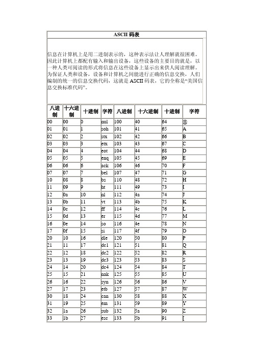
字符
34 35 36 37 40 41 42 43 44 45 46 47 50 51 52 53 54 55 56 57 60 61 62 63 64 65 66 67 70 71 72 73 74 75 76 77
1c 1d 1e 1f 20 21 22 23 24 25 26 27 28 29 2a 2b 2c 2d 2e 2f 30 31 32 33 34 35 36 37 38 39 3a 3b 3c 3d 3e 3f
十六进制 40 41 42 43 44 45 46 47 48 49 4a 4b 4c 4d 4e 4f 50 51 52 53 54 55 56 57 58 59 5a 5b
十进制 64 65 66 67 68 69 70 71 72 73 74 75 76 77 78 79 80 81 82 83 84 85 86 87 88 89 90 91 @ A B C D E F G H I J K L M N O P Q R S T U V W X Y Z [
92 93 94 95 96 97 98 99 100 101 102 103 104 105 106 107 108 109 110 111 112 113 114 115 116 117 118 119 120 121 122 123 124 125 126 127
\ ] ^ _ ' a b c d e f g h i j k l m n o p q r s t u v w x y z { | } ~ del
八进 制 00 01 02 03 04 05 06 07 10 11 12 13 14 15 16 17 20 21 22 23 24 25 26 27 30 31 32 33
十六进 十进制 制 00 0 01 1 02 2 03 3 04 4 05 5 06 6 07 7 08 8 09 9 0a 10 0b 11 0c 12 0d 13 0e 14 0f 15 10 16 11 17 12 18 13 19 14 20 15 21 16 22 17 23 18 24 19 25 1a 26 1b 27
维沙亚高速塑料接收器数据手册说明书

Soft Recovery Ultrafast Plastic RectifierFEATURES•Glass passivated pellet chip junction •Ultrafast reverse recovery time •Low forward voltage drop•Low switching losses, high efficiency •High forward surge capability•Solder dip 275 °C max. 10 s, per JESD 22-B106•Material categorization: for definitions of compliance please see /doc?99912TYPICAL APPLICATIONSFor use in high frequency rectification and freewheeling application in switching mode converters and inverters for consumer, computer and telecommunication.MECHANICAL DATACase: DO-201ADMolding compound meets UL 94 V-0 flammability rating Base P/N-E3 - RoHS-compliant, commercial gradeTerminals: Matte tin plated leads, solderable per J-STD-002 and JESD 22-B102E3 suffix meets JESD 201 class 1A whisker test Polarity: Color band denotes cathode endPRIMARY CHARACTERISTICSI F(AV) 3.0 AV RRM 50 V, 100 V, 200 V, 300 V, 400 V, 500 V, 600 V, 800 V, 1000 VI FSM 150 A t rr 50 ns, 75 ns V F 1.0 V, 1.7 V T J max.150 °C Package DO-201ADDiode variationsSingle dieDO-201ADMAXIMUM RATINGS (T A = 25 °C unless otherwise noted)PARAMETERSYMBOL UF5400UF5401UF5402UF5403UF5404UF5405UF5406UF5407UF5408UNIT Maximum repetitive peak reverse voltage V RRM 501002003004005006008001000V Maximum RMS voltage V RMS 3570140210280350420560700V Maximum DC blocking voltage V DC 501002003004005006008001000V Maximum average forwardrectified current, 0.375" (9.5 mm) lead length at T A = 55 °C I F(AV)3.0APeak forward surge current 8.3 ms single half sine-wave superimposed on rated load I FSM 150AOperating junction and storage temperature rangeT J , T STG-55 to +150°CNote(1)Pulse test: 300 μs pulse width, 1 % duty cycleNote(1)Thermal resistance from junction to lead and from junction to ambient with 0.375" (9.5 mm) lead length, both leads attached to heatsinkRATINGS AND CHARACTERISTICS CURVES (T A = 25 °C unless otherwise noted)Fig. 1 - Maximum Forward Current Derating Curve Fig. 2 - Forward Power Loss CharacteristicsELECTRICAL CHARACTERISTICS (T A = 25 °C unless otherwise noted)PARAMETER TEST CONDITIONS SYMBOL UF5400UF5401UF5402UF5403UF5404UF5405UF5406UF5407UF5408UNITMaximum instantaneous forward voltage 3.0 AV F (1)1.01.7VMaximum DC reverse current at rated DCblocking voltage T A = 25 °CI R10μAT A = 100 °C 75200Maximumreverse recovery timeI F = 0.5 A, I R = 1.0 A, I rr = 0.25 AT J = 25 °Ct rr 5075nsTypical junction capacitance4.0 V, 1 MHz C J 4536pFTHERMAL CHARACTERISTICS (T A = 25 °C unless otherwise noted)PARAMETERSYMBOL UF5400UF5401 UF5402 UF5403 UF5404 UF5405 UF5406 UF5407 UF5408 UNIT Typical thermal resistanceR θJA (1)20°C/WR θJL (1)8.5ORDERING INFORMATION (Example)PREFERRED P/N UNIT WEIGHT (g)PREFERRED PACKAGE CODEBASE QUANTITYDELIVERY MODEUF5406-E3/54 1.17254140013" diameter paper tape and reelUF5406-E3/731.172731000Ammo pack packagingFig. 3 - Maximum Non-Repetitive Peak Forward Surge Current Fig. 4 - Typical Instantaneous Forward Characteristics Fig. 5 - Typical Reverse Leakage CharacteristicsFig. 6 - Typical Junction CapacitancePACKAGE OUTLINE DIMENSIONS in inches (millimeters)Legal Disclaimer Notice VishayDisclaimerALL PRODUCT, PRODUCT SPECIFICAT IONS AND DAT A ARE SUBJECT T O CHANGE WIT HOUT NOT ICE T O IMPROVE RELIABILITY, FUNCTION OR DESIGN OR OTHERWISE.Vishay Intertechnology, Inc., its affiliates, agents, and employees, and all persons acting on its or their behalf (collectively, “Vishay”), disclaim any and all liability for any errors, inaccuracies or incompleteness contained in any datasheet or in any other disclosure relating to any product.Vishay makes no warranty, representation or guarantee regarding the suitability of the products for any particular purpose or the continuing production of any product. To the maximum extent permitted by applicable law, Vishay disclaims (i) any and all liability arising out of the application or use of any product, (ii) any and all liability, including without limitation special, consequential or incidental damages, and (iii) any and all implied warranties, including warranties of fitness for particular purpose, non-infringement and merchantability.Statements regarding the suitability of products for certain types of applications are based on Vishay’s knowledge of typical requirements that are often placed on Vishay products in generic applications. Such statements are not binding statements about the suitability of products for a particular application. It is the customer’s responsibility to validate that a particular product with the properties described in the product specification is suitable for use in a particular application. Parameters provided in datasheets and / or specifications may vary in different applications and performance may vary over time. All operating parameters, including typical parameters, must be validated for each customer application by the customer’s technical experts. Product specifications do not expand or otherwise modify Vishay’s terms and conditions of purchase, including but not limited to the warranty expressed therein.Except as expressly indicated in writing, Vishay products are not designed for use in medical, life-saving, or life-sustaining applications or for any other application in which the failure of the Vishay product could result in personal injury or death. Customers using or selling Vishay products not expressly indicated for use in such applications do so at their own risk. Please contact authorized Vishay personnel to obtain written terms and conditions regarding products designed for such applications.No license, express or implied, by estoppel or otherwise, to any intellectual property rights is granted by this document or by any conduct of Vishay. Product names and markings noted herein may be trademarks of their respective owners.© 2017 VISHAY INTERTECHNOLOGY, INC. ALL RIGHTS RESERVED。
MAS3132E中文资料

Switching Diodes
MAS3132E
Silicon epitaxial planar type
Unit: mm
For high-speed switching circuits ■ Features
• Two elements are contained in one package, allowing highdensity mounting • Short reverse recovery time trr • Small terminal capacitance Ct
0.33+0.05 –0.02 3
0.10+0.05 –0.02
(0.40) (0.40) 0.80±0.05 1.20±0.05 5˚
0 to 0.01
Parameter Reverse voltage Maximum peak reverse voltage Forward current Single Double Peak forward current Single Double Non-repetitive peak forward surge current
1
2
■ Electrical Characteristics Ta = 25°C ± 3°C
Parameter Forward voltage Reverse voltage Reverse current Terminal capacitance Reverse recovery time
*
Symbol VF VR IR Ct trr IR = 100 µA VR = 75 V
1
元器件交易网
MAS3132E
UPC8152TA-E3资料

ORDERING INFORMATIONPart NumberPackage Marking Feature Supplying FormP PC8128TA-E3C2P 2.8 mA Low I CC P PC8151TA-E3C2U 4 mA High P O P PC8152TA-E36-pin minimoldC2V5 mA High G PEmbossed tape 8 mm wide.1, 2, 3 pins face the perforation side of the tape.Qty 3 kpcs/reel.Remark To order evaluation samples, please contact your local NEC sales office.(Part number for sample order:P PC8128TA, P PC8151TA, P PC8152TA)PIN CONNECTIONSPin No.Pin Name 1INPUT 2GND 3GND 4OUTPUT 5GND 6V CC3214C 2P(Top View)Marking is an example of PC8128TA µ564563(Bottom View)21PRODUCT LINE-UP (T A = +25 °C, V CC = V out = 3.0 V, Z S = Z L = 50 :)Remark Typical performance. Please refer to ELECTRICAL CHARACTERISTICS in detail.SYSTEM APPLICATION EXAMPLELocation examples in digital cellularI QThese ICs can be added to your system around v parts, when you need more isolation or gain. The application herein, however, shows only examples, therefore the application can depend on your kit evaluation.PIN EXPLANATIONNote Pin voltage is measured at V CC = 3.0 V. Above: P PC8128TA, Center: P PC8151TA, Below: P PC8152TAABSOLUTE MAXIMUM RATINGSParameter Symbol Conditions Ratings Unit Supply Voltage V CC T A = +25 °C, Pin 4, Pin 6 3.6V Total Circuit Current I CC T A = +25 °C15mA280mW Total Power Dissipation P D Mounted on double sided copper clad 50 u 50 u 1.6mm epoxy glass PWB (T A = +85 °C)Operating Ambient Temperature T Að40 to +85°C Storage Temperature T stgð55 to +150°C Input Power P in T A = +25 °C+5dBm RECOMMENDED OPERATING CONDITIONSParameter Symbol MIN.TYP.MAX.Unit RemarksSupply Voltage V CC 2.4 3.0 3.3V The same voltage should be appliedto pin 4 and pin 6.Operating Ambient Temperature T Að40+25+85°COperating Frequency f0.1ð 1.9GHz Matched output port with external LCELECTRICAL CHARACTERISTICS (Unless otherwise specified, T A = +25 °C, V CC = V out = 3.0 V,Z S = Z L = 50 :, at LC matched frequency)P PC8128TA P PC8151TA P PC8152TA Parameter Symbol TestConditions MIN.TYP.MAX.MIN.TYP.MAX.MIN.TYP.MAX.Unit Circuit Current I CC No signal 1.8 2.8 3.8 2.8 4.2 5.8 4.2 5.67.1mA Power GainG Pf = 1.00 GHz f = 1.66 GHz f = 1.90 GHz 9.5101012.5131314.515159.5121212.5151514.517172016.514.52319.517.52521.519.5dBIsolation ISL f = 1.00 GHz f = 1.66 GHz f = 1.90 GHz 343432393937ððð333129383634ððð353330403835ðððdBGain 1 dB Compression Output Power P O (1 dB) f = 1.00 GHz f = 1.66 GHz f = 1.90 GHz ð7.5ð8.5ð8.5ð4.0ð4.0ð4.0ðððð1.0ð2.5ð3.0+2.5+1.5+0.5ðððð7.5ð11.5ð11.5ð4.5ð8.5ð8.5ðððdBmSaturated OutputPower Note(P in = ð6 dBm)P O (sat) f = 1.00 GHz f = 1.66 GHz f = 1.90 GHz ððððððððððððððððððð2.5ð5.5ð6.0+0.5ð2.5ð3.0ðððdBmNoise FigureNF f = 1.00 GHz f = 1.66 GHz f = 1.90 GHz ððð 6.06.06.07.57.57.5ððð 6.06.06.07.57.57.5ððð 3.54.04.5 5.05.56.0dBInput Return Loss (Withoutmatching circuit)RL in f = 1.00 GHz f = 1.66 GHz f = 1.90 GHz222.5555.5ððð211544ððð8.57.58.511.510.511.5ðððdBNote Saturated output power is specified only in P PC8152TA which has flat saturated region.STANDARD CHARACTERISTICS (Unless otherwise specified, T A = +25 °C, V CC = V out = 3.0 V,Z S = Z L = 50 :, at LC matched frequency)Reference ValueParameter Symbol ConditionsP PC8128TA P PC8151TA P PC8152TAUnit Output Return Loss(With external matching circuit)RL outf = 1.00 GHz f = 1.66 GHz f = 1.90 GHz102514101812157.57dB3rd OrderIntermodulation Distortionõ32õHDFKô ðëíG%PôIM 3f 1 = 1.000 GHz, f 2 = 1.001 GHz f 1 = 1.660 GHz, f 2 = 1.661 GHz f 1 = 1.900 GHz, f 2 = 1.901 GHzð50ð46ð46ð62ð56ð54ð51ð43ð42dBcNOTES ON CORRECT USE(1)Observe precautions for handling because of electro-static sensitive devices.(2)Form a ground pattern as wide as possible to minimize ground impedance (to prevent undesired oscillation).All the ground pins must be connected together with wide ground pattern to decrease impedance difference.(3)The bypass capacitor should be attached to V CC line.(4)The inductor (L) should be attached between output and V CC pins. The L and series capacitor (C2) valuesshould be adjusted for applied frequency to match impedance to next stage.(5)The DC capacitor must be attached to input pin.RECOMMENDED SOLDERING CONDITIONSThis product should be soldered under the following recommended conditions. For soldering methods and conditions other than those recommended below, contact your NEC sales representative.Soldering Method Soldering Conditions Recommended Condition SymbolIR35-00-3Infrared Reflow Package peak temperature: 235 °C or belowTime: 30 seconds or less (at 210 °C)Count: 3, Exposure limit: None NoteVP15-00-3VPS Package peak temperature: 215 °C or belowTime: 40 seconds or less (at 200 °C)Count: 3, Exposure limit: None NoteWS60-00-1Wave Soldering Soldering bath temperature: 260 °C or belowTime: 10 seconds or lessCount: 1, Exposure limit: None NotePartial Heating Pin temperature: 300 °C–Time: 3 seconds or less (per side of device)Exposure limit: None NoteNote After opening the dry pack, keep it in a place below 25 °C and 65 % RH for the allowable storage period.Caution Do not use different soldering methods together (except for partial heating).For details of recommended soldering conditions for surface mounting, refer to information document SEMICONDUCTOR DEVICE MOUNTING TECHNOLOGY MANUAL (C10535E).[MEMO][MEMO][MEMO]。
最全ASCII码对照表

最全ASCII码对照表2009-04-15 00:00Bin Dec Hex 缩写/字符解释0000 0000 0 00 NUL (null) 空字符0000 0001 1 01 SOH (start of handing) 标题开始0000 0010 2 02 STX (start of text) 正文开始0000 0011 3 03 ETX (end of text) 正文结束0000 0100 4 04 EOT (end of transmission) 传输结束0000 0101 5 05 ENQ (enquiry) 请求0000 0110 6 06 ACK (acknowledge) 收到通知0000 0111 7 07 BEL (bell) 响铃0000 1000 8 08 BS (backspace) 退格0000 1001 9 09 HT (horizontal tab) 水平制表符0000 1010 10 0A LF (NL line feed, new line) 换行键0000 1011 11 0B VT (vertical tab) 垂直制表符0000 1100 12 0C FF (NP form feed, new page) 换页键0000 1101 13 0D CR (carriage return) 回车键0000 1110 14 0E SO (shift out) 不用切换0000 1111 15 0F SI (shift in) 启用切换0001 0000 16 10 DLE (data link escape) 数据链路转义0001 0001 17 11 DC1 (device control 1) 设备控制1 0001 0010 18 12 DC2 (device control 2) 设备控制2 0001 0011 19 13 DC3 (device control 3) 设备控制3 0001 0100 20 14 DC4 (device control 4) 设备控制4 0001 0101 21 15 NAK (negative acknowledge) 拒绝接收0001 0110 22 16 SYN (synchronous idle) 同步空闲0001 0111 23 17 ETB (end of trans. block) 传输块结束0001 1000 24 18 CAN (cancel) 取消0001 1001 25 19 EM (end of medium) 介质中断0001 1010 26 1A SUB (substitute) 替补0001 1011 27 1B ESC (escape) 溢出0001 1100 28 1C FS (file separator) 文件分割符0001 1101 29 1D GS (group separator) 分组符0001 1110 30 1E RS (record separator) 记录分离符0001 1111 31 1F US (unit separator) 单元分隔符0010 0000 32 20 空格0010 0001 33 21 !0010 0010 34 22 "0010 0011 35 23 #0010 0100 36 24 $0010 0101 37 25 %0010 0110 38 26 &0010 0111 39 27 '0010 1000 40 28 (0010 1001 41 29 )0010 1101 45 2D - 0010 1110 46 2E . 0010 1111 47 2F / 0011 0000 48 30 0 0011 0001 49 31 1 0011 0010 50 32 2 0011 0011 51 33 3 0011 0100 52 34 4 0011 0101 53 35 5 0011 0110 54 36 6 0011 0111 55 37 7 0011 1000 56 38 8 0011 1001 57 39 9 0011 1010 58 3A : 0011 1011 59 3B ; 0011 1100 60 3C < 0011 1101 61 3D = 0011 1110 62 3E > 0011 1111 63 3F ? 0100 0000 64 40 @ 0100 0001 65 41 A 0100 0010 66 42 B 0100 0011 67 43 C 0100 0100 68 44 D 0100 0101 69 45 E 0100 0110 70 46 F 0100 0111 71 47 G 0100 1000 72 48 H 0100 1001 73 49 I 0100 1010 74 4A J 0100 1011 75 4B K 0100 1100 76 4C L 0100 1101 77 4D M 0100 1110 78 4E N 0100 1111 79 4F O 0101 0000 80 50 P 0101 0001 81 51 Q 0101 0010 82 52 R 0101 0011 83 53 S 0101 0100 84 54 T 0101 0101 85 55 U 0101 0110 86 56 V 0101 0111 87 57 W 0101 1000 88 58 X0101 1100 92 5C \0101 1101 93 5D ]0101 1110 94 5E ^0101 1111 95 5F _0110 0000 96 60 `0110 0001 97 61 a0110 0010 98 62 b0110 0011 99 63 c0110 0100 100 64 d0110 0101 101 65 e0110 0110 102 66 f0110 0111 103 67 g0110 1000 104 68 h0110 1001 105 69 i0110 1010 106 6A j0110 1011 107 6B k0110 1100 108 6C l0110 1101 109 6D m0110 1110 110 6E n0110 1111 111 6F o0111 0000 112 70 p0111 0001 113 71 q0111 0010 114 72 r0111 0011 115 73 s0111 0100 116 74 t0111 0101 117 75 u0111 0110 118 76 v0111 0111 119 77 w0111 1000 120 78 x0111 1001 121 79 y0111 1010 122 7A z0111 1011 123 7B {0111 1100 124 7C |0111 1101 125 7D }0111 1110 126 7E ~0111 1111 127 7F DEL (delete) 删除ESC键VK_ESCAPE (27)回车键:VK_RETURN (13)TAB键:VK_TAB (9)Caps Lock键:VK_CAPITAL (20)Shift键:VK_SHIFT ()Ctrl键:VK_CONTROL (17)Alt键:VK_MENU (18)空格键:VK_SPACE (/32)退格键:VK_BACK (8)左徽标键:VK_LWIN (91)右徽标键:VK_LWIN (92)鼠标右键快捷键:VK_APPS (93) Insert键:VK_INSERT (45) Home键:VK_HOME (36) Page Up:VK_PRIOR (33) PageDown:VK_NEXT (34)End键:VK_END (35)Delete键:VK_DELETE (46)方向键(←):VK_LEFT (37)方向键(↑):VK_UP (38)方向键(→):VK_RIGHT (39)方向键(↓):VK_DOWN (40)F1键:VK_F1 (112)F2键:VK_F2 (113)F3键:VK_F3 (114)F4键:VK_F4 (115)F5键:VK_F5 (116)F6键:VK_F6 (117)F7键:VK_F7 (118)F8键:VK_F8 (119)F9键:VK_F9 (120)F10键:VK_F10 (121)F11键:VK_F11 (122)F12键:VK_F12 (123)Num Lock键:VK_NUMLOCK (144) 小键盘0:VK_NUMPAD0 (96) 小键盘1:VK_NUMPAD0 (97) 小键盘2:VK_NUMPAD0 (98) 小键盘3:VK_NUMPAD0 (99) 小键盘4:VK_NUMPAD0 (100) 小键盘5:VK_NUMPAD0 (101) 小键盘6:VK_NUMPAD0 (102) 小键盘7:VK_NUMPAD0 (103) 小键盘8:VK_NUMPAD0 (104) 小键盘9:VK_NUMPAD0 (105) 小键盘.:VK_DECIMAL (110) 小键盘*:VK_MULTIPLY (106) 小键盘+:VK_MULTIPLY (107) 小键盘-:VK_SUBTRACT (109) 小键盘/:VK_DIVIDE (111) Pause Break键:VK_PAUSE (19) Scroll Lock键:VK_SCROLL (145)。
- 1、下载文档前请自行甄别文档内容的完整性,平台不提供额外的编辑、内容补充、找答案等附加服务。
- 2、"仅部分预览"的文档,不可在线预览部分如存在完整性等问题,可反馈申请退款(可完整预览的文档不适用该条件!)。
- 3、如文档侵犯您的权益,请联系客服反馈,我们会尽快为您处理(人工客服工作时间:9:00-18:30)。
Vishay BCcomponentsAluminum Capacitors Axial Miniature, Long-LifeFEATURES•Polarized aluminum electrolytic capacitors,non-solid electrolyte•Axial leads, cylindrical aluminum case, insulated with a blue sleeve(case Ø 6.3 x 12.7 and 7.7 x 12.7 mm are moulded with flame retardant plastic material)•Mounting ring version not available in insulated form•Taped versions up to case Ø 15x 30 mm available for automatic insertion•Charge and discharge proof•Long useful life: 2000 to 10 000hours at 105°C, high reliability•High ripple current capability•Miniaturized, high CV-product per unit volume •Lead (Pb)-free versions are RoHS compliantAPPLICATIONS•Industrial, automotive, EDP and telecommunication•Smoothing, filtering, buffering in SMPS; coupling,decoupling, timing•Portable and mobile equipment (small size, low mass)•Stand-by applications•Low mounting height boards, vibration and shock resistantMARKINGThe capacitors are marked (where possible) with the following information:•Rated capacitance (in µF)•Tolerance on rated capacitance, code letter in accordance with IEC 60062 (M for ± 20 %)•Rated voltage (in V)•Upper category temperature (105 °C)•Date code, in accordance with IEC 60062•Code for factory of origin•Name of manufacturer•Band to indicate the negative terminal•‘+’ sign to identify the positive terminal (not for case sizes L < 18 mm)•Series number (138)QUICK REFERENCE DATADESCRIPTION VALUENominal case sizes (Ø D x L in mm)6.3x 12.7to10x 2510x 30to 21x 38Rated capacitance range, C R1.0to 15 000 µFT olerance on C R± 20 %Rated voltage range, U R 6.3to 100V Category temperature range - 40to + 105°C Endurance test at 105°C 1000hours 5000hours Useful life at 105°C 2000hours10 000hoursUseful life at 40°C, I R applied1.3x I R applied: 200 000hours 1.8x I R applied: 500 000hours Shelf life at 0V, 105°C 500hours500hoursBased on sectional specificationIEC 60384-4/EN130300Climatic category IEC 6006840/105/56Vishay BCcomponentsAluminum Capacitors Axial Miniature, Long-LifeDIMENSIONS in millimeters AND AVAILABLE FORMSSELECTION CHART FOR C R , U R AND RELEVANT NOMINAL CASE SIZES (Ø D x L in mm)C R (µF)U R (V)6.31016254050631001.0------- 6.3x12.72.2------- 6.3x 12.74.7------ 6.3x 12.77.7x 12.710--- 6.3x 12.7- 6.3x 12.77.7x 12.76.5x 1822-- 6.3x 12.76.3x 12.7-7.7x 12.76.5x 188 x 1833--- 6.3x 12.77.7x 12.7---47-- 6.3x 12.77.7x 12.76.5x 18-8x 1810x 2568-------10x 30100 6.3x 12.7-7.7x 12.76.5x 188x 1810x 1810x 2512.5x 30150-7.7x 12.7----10x 3015x 302207.7x 12.76.5x 188x 1810x 1810x 25-12.5x 3015x 30330----10x 30-12.5x 3018x 30470 6.5 x 188x 1810x 1810x 2512.5x 30-15x 3018x 38680---10x 3012.5x 30-18x 3021x 38100010x 1810x 2510x 3012.5x 3015x 30-18x 38-1500-10x 3012.5x 3015x 3018x 30-21x 38-220010x 2512.5x 3015x 3018x 3018x 38---3300-15x 3018x 3018x 3821x 38---4700-18x 3018x 3018x 38----6800-18x 3818x 3821x 38----10 000-18x 3821x 38-----15 000-21x 38------NoteDetailed tape dimensions see section ‘PACKAGING’.Table 2MOUNTING RING; DIMENSIONS in millimeters, MASS AND PACKAGING QUANTITIESNOMINAL CASE SIZE Ø D x L CASECODEMOUNTING RING: FORM MRMASS(g)PACKAGINGQUANTITIES Ø d1Ød2 D max.Ø D2max.D3L max.15x30020.8 1.0+ 0.415.517.516.5± 0.233≈ 11.7200 18x30030.8 1.0+ 0.418.519.518.5± 0.233≈ 12.9240 18x38040.8 1.0+ 0.418.519.518.5± 0.242≈ 19.0100 21x38050.8 1.0+ 0.421.522.521.5± 0.242≈ 24.0100Vishay BCcomponentsAluminum Capacitors Axial Miniature, Long-LifeNoteUnless otherwise specified, all electrical values in T able 3 apply at T amb =20°C, P =86to 106kPa, RH =45to 75 %.ORDERING EXAMPLEElectrolytic capacitor 138series 470µF/10V;± 20 %Nominal case size: Ø 8 x 18mm; Form BA Ordering code: MAL213834471E3Former 12 NC: 222213834471Table 3ELECTRICAL DATASYMBOL DESCRIPTIONC R rated capacitance at 100Hz, tolerance ± 20 %I R rated RMS ripple current at 100Hz,105°C I L5max. leakage current after 5 minutes at U R tan δmax. dissipation factor at 100Hz ESR equivalent series resistance at 100Hz (calculated from tan δmax. and C R )Z max. impedance at 10kHz or 100kHzELECTRICAL DATA AND ORDERING INFORMATIONU R (V)C R 100HZ (µF)NOMINAL CASE SIZE ØD x L (mm)I R 100 Hz 105 °C (mA)I L55min (µA)tan δ100 Hz ESR 100Hz (Ω)Z 10kHz (Ω)Z100kHz (Ω)ORDERING CODE MAL2138.......IN BOXFORM AATAPED ON REEL FORM BR TAPED IN BOX FORM BA MOUNTING RING FORM MR 6.3100 6.3x 12.799 5.30.24 3.8 3.0 1.8-23101E333101E3-2207.7x 12.7160 6.80.24 1.7 1.40.95-23221E333221E3-470 6.5x 182509.90.240.810.640.5-23471E333471E3-100010x 18430170.240.380.300.24-23102E333102E3-220010x 25640320.290.210.180.15-23222E333222E3-101507.7x 12.71407.00.2 2.1 1.30.95-24151E334151E3-220 6.5x 181908.40.2 1.40.910.5-24221E334221E3-4708x 18300130.20.680.430.35-24471E334471E3-100010x 25520240.20.320.200.16-24102E334102E3-150010x 30670340.280.320.260.2614152E324152E3--220012.5x 30890480.290.220.190.1914222E324222E3--330015x 301140700.300.160.130.1514332E324332E3-44332E3470018x 301450980.330.120.110.1314472E3--44472E3680018x 3818801400.340.0850.0740.1114682E3--44682E310 00018x 3819802000.410.0700.0620.1014103E3--44103E315 00021x 3822003000.550.0630.0580.09914153E3--44153E31622 6.3x 12.758 4.70.128.77.3 2.7-25229E335229E3-47 6.3x 12.783 5.50.16 5.4 3.4 1.9-25479E335479E3-1007.7x 12.71307.20.16 2.5 1.6 1.0-25101E335101E3-2208x 18230110.16 1.20.730.35-25221E335221E3-47010x 18360190.160.540.340.25-25471E335471E3-100010x 30630360.200.340.270.2615102E325102E3--150012.5x 30860520.200.230.190.1915152E325152E3--220015x 301090740.210.170.140.1515222E325222E3-45222E3330018x 3014201100.240.120.100.1315332E3--45332E3470018x 3014801500.280.100.0900.1215472E3--45472E3680018x 3819302200.280.0720.0620.1015682E3--45682E310 00021x 3821003200.380.0650.0570.09815103E3--45103E32510 6.3x 12.746 4.50.091412 2.8-26109E336109E3-22 6.3x 12.761 5.10.1410 5.5 2.5-26229E336229E3-33 6.3x 12.774 5.70.14 6.8 3.6 1.9-26339E336339E3-477.7x 12.7966.40.144.72.61.0-26479E336479E3-Aluminum CapacitorsAxial Miniature, Long-LifeVishay BCcomponents25100 6.5x181609.00.13 2.1 1.20.55-26101E336101E3-22010x18270150.130.940.550.27-26221E336221E3-47010x25440280.130.440.260.17-26471E336471E3-68010x30580380.140.360.260.2516681E326681E3--100012.5x30790540.150.250.180.1916102E326102E3--150015x301020790.150.170.130.1516152E326152E3-46152E3 220018x3013201100.170.130.100.1316222E3--46222E3 330018x3817201700.170.0900.0710.1116332E3--46332E3 470018x3818402400.210.0760.0630.1016472E3--46472E3 680021x3821003400.270.0680.0580.09916682E3--46682E340337.7x12.791 6.60.11 5.3 2.7 1.0-27339E337339E3-47 6.5x181207.80.10 3.4 1.90.65-27479E337479E3-1008x18180120.10 1.60.90.40-27101E337101E3-22010x25350220.100.720.410.20-27221E337221E3-33010x30490300.090.470.320.3017331E327331E3--47012.5x30650420.090.340.230.2217471E327471E3--68012.5x30750580.100.250.180.1817681E327681E3--100015x30970840.100.170.120.1417102E327102E3-47102E3 150018x3012501200.120.130.0980.1217152E3--47152E3 220018x3816401800.120.0930.0690.1017222E3--47222E3 330021x3818102700.150.0790.0610.1017332E3--47332E35010 6.3x12.751 5.00.09147 2.7-21109E331109E3-227.7x12.782 6.20.09 6.5 3.2 1.1-21229E331229E3-10010x18230140.08 1.30.70.30-21101E331101E3-634.7 6.3x12.735 4.60.0930175- 28478E338478E3-107.7x12.759 5.30.08138 1.8-28109E338109E3-22 6.5x18100 6.80.07 5.1 3.60.85-28229E338229E3-478x181509.90.07 2.4 1.70.50-28479E338479E3-10010x25280170.07 1.10.80.27-28101E338101E3-15010x30410230.110.730.440.4018151E328151E3--22012.5x30560320.110.500.310.2918221E328221E3--33012.5x30660460.120.370.230.2218331E328331E3--47015x30860630.120.260.160.1618471E328471E3-48471E3 68018x301130900.120.190.120.1418681E3--48681E3 100018x3814601300.120.130.0860.1118102E3--48102E3 150021x3816801900.130.100.0720.1118152E3--48152E31001.0 6.3x12.716 4.20.091405510-29108E339108E3-2.2 6.3x12.724 4.40.0965258-29228E339228E3-4.77.7x12.740 4.90.0827175-29478E339478E3-10 6.5x1867 6.00.07118 2.4-29109E339109E3-228x181008.40.07 5.13.6 1.4-29229E339229E3-4710x25190130.07 2.4 1.70.67-29479E339479E3-6810x30300180.07 1.7 1.10.9719689E329689E3--10012.5x30410240.07 1.10.770.6719101E329101E3--15015x30550340.070.780.520.4619151E329151E3-49151E3 22015x30650480.070.540.370.3319221E329221E3-49221E3 33018x30880700.080.380.270.2419331E3--49331E3 47018x381130980.080.270.190.1719471E3--49471E3 68021x3813301400.090.210.140.1419681E3--49681E3ELECTRICAL DATA AND ORDERING INFORMATIONU R (V)C R100HZ(µF)NOMINALCASESIZEØ D x L(mm)I R100 Hz105 °C(mA)I L55min(µA)tan δ100HzESR100Hz(Ω)Z10kHz(Ω)Z100kHz(Ω)ORDERING CODE MAL2138.......IN BOXFORM AATAPEDON REELFORM BRTAPED INBOXFORM BAMOUNTINGRINGFORM MRVishay BCcomponentsAluminum Capacitors Axial Miniature, Long-LifeCAPACITANCE (C)ADDITIONAL ELECTRICAL DATAPARAMETERCONDITIONSVALUEAXIALMOUNTING RINGVoltageSurge voltage U s ≤1.15 x U R Reverse voltage U rev ≤1VCurrentLeakage currentAfter 1minute at U R :case Ø D x L =6.3x 12.7 and 7.7x 12.7mm I L1≤0.02 C R x U R +3µA case Ø D x L=6.5x 18to 21x 38mm I L1≤0.006 C R x U R +4µA After 5minutes at U R I L5≤0.002 C R x U R +4µAInductanceEquivalent series inductance (ESL)Case Ø D x L mm:6.3x 12.7typ. 20nH -7.7x 12.7typ. 30nH -6.5x 18typ. 15nH -8x 18typ. 35nH -10x 18typ. 69nH -10x 25typ. 38nH -10x 30typ. 38nH -12.5x 30typ. 46nH -15x 30typ. 48nH typ. 39nH 18x 30typ. 50nH typ. 39nH 18x 38typ. 54nH typ. 39nH 21x 38typ. 59nHtyp. 39nHT am b (°C)Fig.6 T ypical m u ltiplier of capacitance as a f u nction ofam b ient temperat u re Case Ø D x L = 6.3 x 12.7 to 10 x 25 mm C 0 = typical at 20 °C, 100 Hz0.60.70.80.91.01.1C 0 - 60 - 40 - 20 0 20 40 60 80 100 120T am b (°C)Fig.7 T ypical m u ltiplier of capacitance as a f u nction ofam b ient temperat u reCase Ø D x L = 10 x 30 to 21 x 38 mm C 0 = typical at 20 °C, 100 Hz- 60 - 40 - 20 0 20 40 60 80 100 120Aluminum CapacitorsVishay BCcomponentsAxial Miniature, Long-LifeEQUIVALENT SERIES RESISTANCE (ESR)Vishay BCcomponentsAluminum Capacitors Axial Miniature, Long-LifeEQUIVALENT SERIES RESISTANCE (ESR)IMPEDANCE (Z)Table 4IMPEDANCE VS. CAPACITANCE VALUES (case Ø D x L = 6.3 x 12.7 to 10 x 25 mm)T amb Z x C R (Ωx µF) AT 10kHz6.3V10V 16V 25V 40V 50V 63V 100V + 20°C ≤ 300≤ 200≤ 160≤ 120≤ 90≤ 70≤ 80≤ 80- 25°C ≤ 2000≤ 1200≤ 750≤ 560≤ 450≤ 300≤ 550≤ 550- 40°C≤ 5500≤ 3200≤ 2000≤ 1500≤ 1200≤ 900≤ 1500≤ 1500Aluminum CapacitorsVishay BCcomponents Axial Miniature, Long-LifeVishay BCcomponentsAluminum Capacitors Axial Miniature, Long-LifeRIPPLE CURRENT AND USEFUL LIFETable 5Fig.19 Multiplier of useful life as a function of ambient temperature and ripple current loadMULTIPLIER OF RIPPLE CURRENT (I R ) AS A FUNCTION OF FREQUENCYFREQUENCY(Hz)I R MULTIPLIERU R =6.3to 10VU R =16to 25VU R =40to 100V500.950.900.85100 1.00 1.00 1.00300 1.07 1.12 1.201000 1.12 1.20 1.303000 1.15 1.25 1.35≥ 10 0001.201.301.40Document Number: 28332For technical questions, contact: aluminumcaps1@Revision: 15-Oct-08215138 AMLAluminum Capacitors Axial Miniature, Long-LifeVishay BCcomponentsTable 6TEST PROCEDURES AND REQUIREMENTSTESTPROCEDURE (quick reference)REQUIREMENTSNAME OF TEST REFERENCE EnduranceIEC 60384-4/EN130300subclause 4.13T amb =105°C; U R applied;case Ø D x L:6.3 x 12.7to 10 x 25mm: 1000hours;10 x 30to 21 x 38mm: 5000hoursU R ≤6.3V; ΔC/C:+ 15/- 30 %U R >6.3V; ΔC/C:± 15 %tan δ≤1.3x spec. limit Z ≤2x spec. limit I L5≤spec. limitUseful lifeCECC 30301subclause 1.8.1T amb =105°C; U R and I R applied;case Ø D x L:6.3x 12.7to 10x 25mm: 2000hours;10x 30to 21x 38mm: 10 000hoursU R ≤6.3V; ΔC/C:+ 45/- 50 %U R >6.3V; ΔC/C:± 45 %tan δ≤3x spec. limit Z ≤3x spec. limit I L5≤spec. limit no short or open circuit total failure percentage: ≤ 1 %Shelf life (storage at high temperature)IEC 60384-4/EN130300,subclause 4.17T amb =105°C; no voltage applied;500hoursafter test: U R to be applied for 30minutes, 24to 48hours before measurementΔC/C, tan δ, Z: for requirementssee ‘Endurance test’ above I L5≤2x spec. limit元器件交易网Document Number: 91000Revision: 18-Jul-081DisclaimerLegal Disclaimer NoticeVishayAll product specifications and data are subject to change without notice.Vishay Intertechnology, Inc., its affiliates, agents, and employees, and all persons acting on its or their behalf (collectively, “Vishay”), disclaim any and all liability for any errors, inaccuracies or incompleteness contained herein or in any other disclosure relating to any product.Vishay disclaims any and all liability arising out of the use or application of any product described herein or of any information provided herein to the maximum extent permitted by law. The product specifications do not expand or otherwise modify Vishay’s terms and conditions of purchase, including but not limited to the warranty expressed therein, which apply to these products.No license, express or implied, by estoppel or otherwise, to any intellectual property rights is granted by this document or by any conduct of Vishay.The products shown herein are not designed for use in medical, life-saving, or life-sustaining applications unless otherwise expressly indicated. Customers using or selling Vishay products not expressly indicated for use in such applications do so entirely at their own risk and agree to fully indemnify Vishay for any damages arising or resulting from such use or sale. Please contact authorized Vishay personnel to obtain written terms and conditions regarding products designed for such applications.Product names and markings noted herein may be trademarks of their respective owners.元器件交易网。