DS32EV400SQ中文资料
400W LDMOS S-带雷达应用电磁性功能芯片说明书

BLS9G3135L-400;BLS9G3135LS-400LDMOS S-band radar power transistorRev. 1 — 6 April 2017Product data sheet 1. Product profile1.1General description400W LDMOS power transistor for S-band radar applications in the frequency range from3.1 GHz to 3.5 GHz.Table 1.Typical performanceTypical RF performance at T case=25︒C; t p = 300 μs; δ = 10%; I Dq = 400 mA; in a class-AB democircuit.Test signal f V DS P L G pηD(GHz)(V)(W)(dB)(%)pulsed RF 3.1 to 3.53242512431.2Features and benefits⏹High efficiency⏹Excellent ruggedness⏹Designed for S-band operation⏹Excellent thermal stability⏹Easy power control⏹Integrated dual sided ESD protection enables excellent off-state isolation⏹High flexibility with respect to pulse formats⏹Internally matched for ease of use⏹Compliant to Directive 2002/95/EC, regarding Restriction of Hazardous Substances(RoHS)1.3Applications⏹S-band radar applications in the frequency range 3.1 GHz to3.5GHz2. Pinning informationTable 2.Pinning[1]Connected to flange.3. Ordering informationTable 3.Ordering informationType number PackageName Description Version BLS9G3135L-400-flanged ceramic package; 2mounting holes; 2leads SOT502ABLS9G3135LS-400-earless flanged ceramic package; 2leads SOT502B 4. Limiting valuesTable 4.Limiting valuesIn accordance with the Absolute Maximum Rating System (IEC 60134).Symbol Parameter Min Max UnitV DS drain-source voltage-65VV GS gate-source voltage-6+11VT stg storage temperature-65+150︒CT j junction temperature[1]-225︒C[1]Continuous use at maximum temperature will affect the reliability. For details refer to the online MTFcalculator.5. Thermal characteristics6. CharacteristicsTable 5.Thermal characteristicsSymbol ParameterConditionsTypUnitZ th(j-mb)transient thermal impedance from junction to mounting baseT case =85︒C; P L =400Wt p =100μs; δ = 10%0.11K/W t p =200μs; δ = 10%0.13K/W t p =300μs; δ = 10%0.15K/W t p =500μs; δ = 10%0.17K/W t p =1ms; δ = 10%0.18K/W t p =100μs; δ = 20%0.15K/WTable 6.DC characteristicsT j =25︒C unless otherwise specified.Symbol ParameterConditionsMin Typ Max Unit V (BR)DSS drain-source breakdown voltage V GS =0V; I D =4.5mA 65--V V GS(th)gate-source threshold voltage V DS =10 V; I D =450mA 1.52 3.1V I DSS drain leakage current V GS =0V; V DS =28V --4μA I DSX drain cut-off current V GS =V GS(th)+3.75 V; V DS =10V-85-A I GSS gate leakage current V GS =11V; V DS =0V --400nA g fs forward transconductance V DS =10V; I D =450mA - 4.2-S R DS(on)drain-source on-state resistanceV GS =V GS(th) + 3.75V; I D =15.75A-0.026-ΩTable 7.RF characteristicsTest signal: pulsed RF; t p = 300 μs; δ = 10%; RF performance at V DS =32V;I Dq =400mA; T case =25︒C; unless otherwise specified, in a class-AB production circuit.Symbol Parameter Conditions Min Typ Max Unit G p power gain P L =425W 1011-dB ηD drain efficiency P L =425W 4043-%RL ininput return loss P L =425W --6-dB P droop(pulse)pulse droop power P L =425W -0.150.50dB t r rise time P L =425W -650ns t f fall timeP L =425W-650ns P L(2dB)output power at 2 dB gain compression400--W7. Test information7.1Ruggedness in class-AB operationThe BLS9G3135L-400 and BLS9G3135LS-400 are capable of withstanding a loadmismatch corresponding to VSWR=10:1 through all phases under the followingconditions: V DS=32V; I Dq=400mA; P L=400W; t p = 300 μs; δ = 10%.7.2Impedance informationTable 8.Typical impedancef Z S Z L(GHz)(Ω)(Ω)3.14.122 - j8.679 1.206 - j4.2313.2 6.215 - j3.927 1.593 - j4.3963.34.334 - j3.313 1.885 - j4.2623.4 2.085 - j2.187 2.473 - j3.9153.5 1.976 - j2.700 2.313 - j3.1807.3Test circuit informationTable 9.List of componentsFor test circuit see Figure2.Component Description Value RemarksC1, C4multilayer ceramic chip capacitor10pF ATC100AC2multilayer ceramic chip capacitor 4.7μFC3, C8, C10multilayer ceramic chip capacitor1nF ATC100BC5, C6, C9multilayer ceramic chip capacitor10pF ATC800AC7, C11multilayer ceramic chip capacitor10μF, 50 V Murata: GRM55DR61H106KA88L C12electrolytic capacitor220μF, 63 VR1resistor5ΩSMD 06037.4Graphical data8. Package outlineFlanged ceramic package; 2 mounting holes; 2 leads SOT502AFig 8.Package outline SOT502AEarless flanged ceramic package; 2 leads SOT502BFig 9.Package outline SOT502B9. Handling informationTable 10.ESD sensitivityESD model ClassCharged Device Model (CDM); According to ANSI/ESDA/JEDEC standard JS-002C2A [1]Human Body Model (HBM); According to ANSI/ESDA/JEDEC standard JS-001 2 [2][1]CDM classification C2A is granted to any part that passes after exposure to an ESD pulse of 500V, but failsafter exposure to an ESD pulse of 750V.[2]HBM classification 2 is granted to any part that passes after exposure to an ESD pulse of 2000V, but failsafter exposure to an ESD pulse of 4000V.10. AbbreviationsTable 11.AbbreviationsAcronym DescriptionESD ElectroStatic DischargeLDMOS Laterally Diffused Metal-Oxide SemiconductorMTF Median Time to FailureS-band Short wave BandSMD Surface Mounted DeviceVSWR Voltage Standing-Wave Ratio11. Revision historyTable 12.Revision historyDocument ID Release date Data sheet status Change notice SupersedesBLS9G3135L-400_LS-400 v.120170406Product data sheet--12. Legal information12.1 Data sheet status[1]Please consult the most recently issued document before initiating or completing a design.[2]The term ‘short data sheet’ is explained in section “Definitions”.[3]The product status of device(s) described in this document may have changed since this document was published and may differ in case of multiple devices. The latest product statusinformation is available on the Internet at URL .12.2 DefinitionsDraft — The document is a draft version only. The content is still under internal review and subject to formal approval, which may result in modifications or additions. Ampleon does not give any representations or warranties as to the accuracy or completeness of information included herein and shall have no liability for the consequences of use of such information.Short data sheet — A short data sheet is an extract from a full data sheet with the same product type number(s) and title. A short data sheet is intended for quick reference only and should not be relied upon to contain detailed and full information. For detailed and full information see the relevant full data sheet, which is available on request via the local Ampleon sales office. In case of any inconsistency or conflict with the short data sheet, the full data sheet shall prevail.Product specification — The information and data provided in a Product data sheet shall define the specification of the product as agreed between Ampleon and its customer, unless Ampleon and customer have explicitly agreed otherwise in writing. In no event however, shall an agreement be valid in which the Ampleon product is deemed to offer functions and qualities beyond those described in the Product data sheet.12.3 DisclaimersLimited warranty and liability — Information in this document is believed to be accurate and reliable. However, Ampleon does not give any representations or warranties, expressed or implied, as to the accuracy or completeness of such information and shall have no liability for the consequences of use of such information. Ampleon takes no responsibility for the content in this document if provided by an information source outside of Ampleon.In no event shall Ampleon be liable for any indirect, incidental, punitive, special or consequential damages (including - without limitation - lost profits, lost savings, business interruption, costs related to the removal or replacement of any products or rework charges) whether or not such damages are based on tort (including negligence), warranty, breach of contract or any other legal theory.Notwithstanding any damages that customer might incur for any reason whatsoever, Ampleon’s aggregate and cumulative liability towards customer for the products described herein shall be limited in accordance with the Terms and conditions of commercial sale of Ampleon.Right to make changes — Ampleon reserves the right to make changes to information published in this document, including without limitation specifications and product descriptions, at any time and without notice. This document supersedes and replaces all information supplied prior to the publication hereof.Suitability for use — Ampleon products are not designed, authorized or warranted to be suitable for use in life support, life-critical or safety-critical systems or equipment, nor in applications where failure or malfunction of an Ampleon product can reasonably be expected to result in personal injury, death or severe property or environmental damage. Ampleon and its suppliers accept no liability for inclusion and/or use of Ampleon products in such equipment or applications and therefore such inclusion and/or use is at the customer’s own risk.Applications — Applications that are described herein for any of these products are for illustrative purposes only. Ampleon makes no representation or warranty that such applications will be suitable for the specified use without further testing or modification.Customers are responsible for the design and operation of their applications and products using Ampleon products, and Ampleon accepts no liability for any assistance with applications or customer product design. It is customer’s sole responsibility to determine whether the Ampleon product is suitable and fit for the customer’s applications and products planned, as well as for the planned application and use of customer’s third party customer(s). Customers should provide appropriate design and operating safeguards to minimize the risks associated with their applications and products.Ampleon does not accept any liability related to any default, damage, costs or problem which is based on any weakness or default in the customer’s applications or products, or the application or use by customer’s third party customer(s). Customer is responsible for doing all necessary testing for the customer’s applications and products using Ampleon products in order to avoid a default of the applications and the products or of the application or use by customer’s third party customer(s). Ampleon does not accept any liability in this respect.Limiting values — Stress above one or more limiting values (as defined in the Absolute Maximum Ratings System of IEC60134) will cause permanent damage to the device. Limiting values are stress ratings only and (proper) operation of the device at these or any other conditions above those given in the Recommended operating conditions section (if present) or the Characteristics sections of this document is not warranted. Constant or repeated exposure to limiting values will permanently and irreversibly affect the quality and reliability of the device.Terms and conditions of commercial sale — Ampleon products are sold subject to the general terms and conditions of commercial sale, as published at /terms, unless otherwise agreed in a valid written individual agreement. In case an individual agreement is concluded only the terms and conditions of the respective agreement shall apply. Ampleon hereby expressly objects to applying the customer’s general terms and conditions with regard to the purchase of Ampleon products by customer.No offer to sell or license — Nothing in this document may be interpreted or construed as an offer to sell products that is open for acceptance or the grant, conveyance or implication of any license under any copyrights, patents or other industrial or intellectual property rights.Export control — This document as well as the item(s) described herein may be subject to export control regulations. Export might require a prior authorization from competent authorities.Document status[1][2]Product status[3]DefinitionObjective [short] data sheet Development This document contains data from the objective specification for product development. Preliminary [short] data sheet Qualification This document contains data from the preliminary specification.Product [short] data sheet Production This document contains the product specification.Non-automotive qualified products — Unless this data sheet expressly states that this specific Ampleon product is automotive qualified, the product is not suitable for automotive use. It is neither qualified nor tested in accordance with automotive testing or application requirements. Ampleon accepts no liability for inclusion and/or use of non-automotive qualified products in automotive equipment or applications.In the event that customer uses the product for design-in and use in automotive applications to automotive specifications and standards, customer (a) shall use the product without Ampleon’ warranty of the product for such automotive applications, use and specifications, and (b) whenever customer uses the product for automotive applications beyond Ampleon’ specifications such use shall be solely at customer’s own risk, and (c) customer fully indemnifies Ampleon for any liability, damages or failed product claims resulting from customer design and use of the product for automotive applications beyond Ampleon’ standard warranty and Ampleon’ product specifications.Translations — A non-English (translated) version of a document is for reference only. The English version shall prevail in case of any discrepancy between the translated and English versions.12.4 TrademarksNotice: All referenced brands, product names, service names and trademarks are the property of their respective owners.Any reference or use of any ‘NXP’ trademark in this document or in or on the surface of Ampleon products does not result in any claim, liability or entitlement vis-à-vis the owner of this trademark. Ampleon is no longer part of the NXP group of companies and any reference to or use of the ‘NXP’ trademarks will be replaced by reference to or use of Ampleon’s own trademarks.13. Contact informationFor more information, please visit: For sales office addresses, please visit: /sales14. Contents1 Product profile. . . . . . . . . . . . . . . . . . . . . . . . . . 11.1 General description . . . . . . . . . . . . . . . . . . . . . 11.2 Features and benefits. . . . . . . . . . . . . . . . . . . . 11.3 Applications . . . . . . . . . . . . . . . . . . . . . . . . . . . 12 Pinning information. . . . . . . . . . . . . . . . . . . . . . 23 Ordering information. . . . . . . . . . . . . . . . . . . . . 24 Limiting values. . . . . . . . . . . . . . . . . . . . . . . . . . 25 Thermal characteristics . . . . . . . . . . . . . . . . . . 36 Characteristics. . . . . . . . . . . . . . . . . . . . . . . . . . 37 Test information. . . . . . . . . . . . . . . . . . . . . . . . . 47.1 Ruggedness in class-AB operation . . . . . . . . . 47.2 Impedance information. . . . . . . . . . . . . . . . . . . 47.3 Test circuit information . . . . . . . . . . . . . . . . . . . 57.4 Graphical data . . . . . . . . . . . . . . . . . . . . . . . . . 68 Package outline. . . . . . . . . . . . . . . . . . . . . . . . . 89 Handling information. . . . . . . . . . . . . . . . . . . . 1010 Abbreviations. . . . . . . . . . . . . . . . . . . . . . . . . . 1011 Revision history. . . . . . . . . . . . . . . . . . . . . . . . 1012 Legal information. . . . . . . . . . . . . . . . . . . . . . . 1112.1 Data sheet status . . . . . . . . . . . . . . . . . . . . . . 1112.2 Definitions. . . . . . . . . . . . . . . . . . . . . . . . . . . . 1112.3 Disclaimers. . . . . . . . . . . . . . . . . . . . . . . . . . . 1112.4 Trademarks. . . . . . . . . . . . . . . . . . . . . . . . . . . 1213 Contact information. . . . . . . . . . . . . . . . . . . . . 1214 Contents. . . . . . . . . . . . . . . . . . . . . . . . . . . . . . 13Please be aware that important notices concerning this document and the product(s)described herein, have been included in section ‘Legal information’.© Ampleon Netherlands B.V.2017.All rights reserved.For more information, please visit: For sales office addresses, please visit: /sales。
ASC-400中文操作手册

3.4 3.5
屏幕上部 (读取数据) – 功能……………………........................................................................................ 12 屏幕下部 (主显示)-功能…………………………........................................................................................ 12
DS32EV400资料
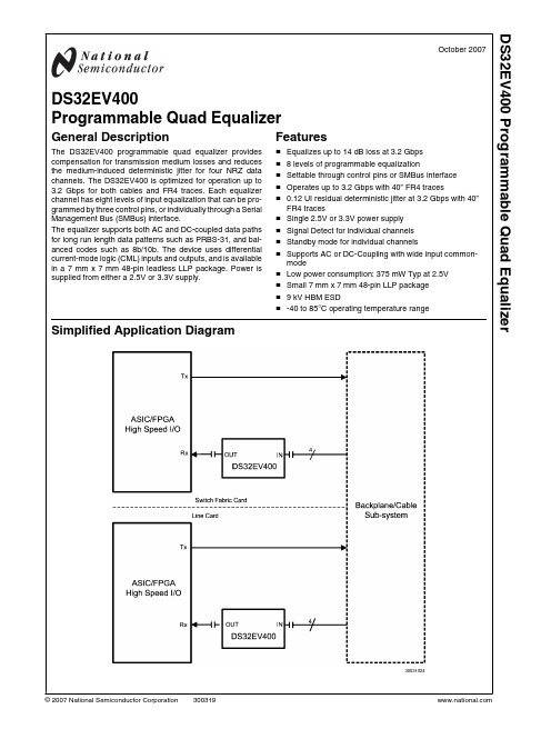
October 2007 DS32EV400Programmable Quad EqualizerGeneral DescriptionThe DS32EV400 programmable quad equalizer provides compensation for transmission medium losses and reduces the medium-induced deterministic jitter for four NRZ data channels. The DS32EV400 is optimized for operation up to 3.2 Gbps for both cables and FR4 traces. Each equalizer channel has eight levels of input equalization that can be pro-grammed by three control pins, or individually through a Serial Management Bus (SMBus) interface.The equalizer supports both AC and DC-coupled data paths for long run length data patterns such as PRBS-31, and bal-anced codes such as 8b/10b. The device uses differential current-mode logic (CML) inputs and outputs, and is available in a 7 mm x 7 mm 48-pin leadless LLP package. Power is supplied from either a 2.5V or 3.3V supply.Features■Equalizes up to 14 dB loss at 3.2 Gbps■8 levels of programmable equalization■Settable through control pins or SMBus interface■Operates up to 3.2 Gbps with 40” FR4 traces■0.12 UI residual deterministic jitter at 3.2 Gbps with 40”FR4 traces■Single 2.5V or 3.3V power supply■Signal Detect for individual channels■Standby mode for individual channels■Supports AC or DC-Coupling with wide input common-mode■Low power consumption: 375 mW Typ at 2.5V■Small 7 mm x 7 mm 48-pin LLP package■9 kV HBM ESD■-40 to 85°C operating temperature rangeSimplified Application Diagram30031924© 2007 National Semiconductor DS32EV400 Programmable Quad EqualizerPin DescriptionsPin Name Pin NumberI/O, Type DescriptionHIGH SPEED DIFFERENTIAL I/OIN_0+IN_0–12I, CML Inverting and non-inverting CML differential inputs to the equalizer. An on-chip 100Ωterminating resistor is connected between IN_0+ and IN_0-.IN_1+IN_1–45I, CML Inverting and non-inverting CML differential inputs to the equalizer. An on-chip 100Ωterminating resistor is connected between IN_1+ and IN_1-.IN_2+IN_2–89I, CML Inverting and non-inverting CML differential inputs to the equalizer. An on-chip 100Ωterminating resistor is connected between IN_2+ and IN_2-.IN_3+IN_3–1112I, CML Inverting and non-inverting CML differential inputs to the equalizer. An on-chip 100Ωterminating resistor is connected between IN_3+ and IN_3-.OUT_0+OUT_0–3635O, CML Inverting and non-inverting CML differential outputs from the equalizer. An on-chip 50Ωterminating resistor connects OUT_0+ to V DD and OUT_0- to V DD .OUT_1+OUT_1–3332O, CML Inverting and non-inverting CML differential outputs from the equalizer. An on-chip 50Ωterminating resistor connects OUT_1+ to V DD and OUT_1- to V DD .OUT_2+OUT_2–2928O, CML Inverting and non-inverting CML differential outputs from the equalizer. An on-chip 50Ωterminating resistor connects OUT_2+ to V DD and OUT_2- to V DD .OUT_3+OUT_3–2625O, CMLInverting and non-inverting CML differential outputs from the equalizer. An on-chip 50Ωterminating resistor connects OUT_3+ to V DD and OUT_3- to V DD .EQUALIZATION CONTROLBST_2BST_1BST_0371423I, CMOSBST_2, BST_1, and BST_0 select the equalizer strength for EQ channel 1. BST_2 is internally pulled high. BST_1 and BST_0 are internally pulled low.DEVICE CONTROLEN044I, CMOS Enable Equalizer Channel 0 input. When held High, normal operation is selected. When held Low, standby mode is selected. EN is internally pulled High.EN142I, CMOS Enable Equalizer Channel 1 input. When held High, normal operation is selected. When held Low, standby mode is selected. EN is internally pulled High.EN240I, CMOS Enable Equalizer Channel 2 input. When held High, normal operation is selected. When held Low, standby mode is selected. EN is internally pulled High.EN338I, CMOS Enable Equalizer Channel 3 input. When held High, normal operation is selected. When held Low, standby mode is selected. EN is internally pulled High.FEB21I, CMOSForce External Boost. When held high, the equalizer boost setting is controlled by BST_[2:0]pins. When held low, the equalizer boost setting is controlled by SMBus (see Table 1) control pins. FEB is internally pulled High.SD045O, CMOS Equalizer Ch0 Signal Detect Output. Produces a High when signal is detected.SD143O, CMOS Equalizer Ch1 Signal Detect Output. Produces a High when signal is detected.SD241O, CMOS Equalizer Ch2 Signal Detect Output. Produces a High when signal is detected.SD339O, CMOS Equalizer Ch3 Signal Detect Output. Produces a High when signal is detected.POWER V DD3, 6, 7,10, 13,15, 46PowerV DD = 2.5V ± 5% or 3.3V ± 10%. V DD pins should be tied to V DD plane through low inductance path. A 0.01μF bypass capacitor should be connected between each V DD pin to GND planes.GND22, 24,27, 30,31, 34PowerGround reference. GND should be tied to a solid ground plane through a low impedance path.Exposed PadPADPowerGround reference. The exposed pad at the center of the package must be connected to ground plane of the board. 2D S 32E V 400Pin Name Pin Number I/O, Type Description SERIAL MANAGEMENT BUS (SMBus) INTERFACE CONTROL PINSSDA SDC CS 181716I, CMOSI, CMOSI, CMOSData input. Internally pulled high.Clock input. Internally pulled high.Chip select. When held high, access to the equalizer SMBus registers are enabled. Whenheld low, access to the equalizer SMBus registers are disabled. CS is internally gated withSDC.OtherReserv19, 2047,48Reserved. Do not connect.Note: I = Input O = OutputConnection Diagram30031926 DS32EV400Absolute Maximum Ratings (Note 1)If Military/Aerospace specified devices are required,please contact the National Semiconductor Sales Office/Distributors for availability and specifications.Supply Voltage (V DD )-0.5V to +4.0V CMOS Input Voltage -0.5V + 4.0V CMOS Output Voltage -0.5V to 4.0V CML Input/Output Voltage -0.5V to 4.0VJunction temperature +150°CStorage temperature-65°C to +150°CLead temperature (Soldering, 4Seconds)+260°CESD ratingHBM, 1.5 k Ω, 100 pF >9 kV EIAJ, 0Ω, 200pF >250VThermal Resistance θJA , no airflow30°C/WRecommended Operating ConditionsMin Typ Max Units Supply Voltage V DD2.5 to GND 2.375 2.5 2.625V V DD3.3 to GND3.0 3.3 3.6V Ambient Temperature-4025+85°CElectrical CharacteristicsOver recommended operating supply and temperature ranges with default register settings unless other specified.Symbol ParameterConditionsMinTypMaxUnitsPOWER P Power Supply Consumption Device Enabled, V DD3.3 490700mW EN0 — EN3 = Low, V DD3.3100mW P Power Supply Consumption Device Enabled, V DD2.5 360490mW EN0 — EN3 = Low, V DD2.5 30 NSupply Noise Tolerance50 Hz — 100 Hz100 Hz — 10 MHz 10 MHz — 1.6 GHz1004010mV P-P mV P-P mV P-PLVTTL DC SPECIFICATIONS V IHHigh Level Input VoltageV DD3.3 2.0 V DD V V DD2.51.6 V DD V V IL Low Level Input Voltage-0.3 0.8V V OH High Level Output Voltage I OH = -3mA, V DD3.3 2.4 V I OH = -3mA, V DD2.5 2.0 V OL Low Level Output Voltage I OL = 3mA 0.4V I IN Input Leakage CurrentV IN = V DD +15μA V IN = GND-15 μA I IN-PInput Leakage Current withInternal Pull-Down/Up ResistorsV IN = V DD , with internal pull-down resistors+120μA V IN = GND, with internal pull-up resistors-20μASIGNAL DETECT SDH Signal Detect High Default input signal level to assert SD pin, 3.2 Gbps75 mV p-p SDISignal Detect LowDefault input signal level to de-assert SD, 3.2Gbps35mV p-pCML RECEIVER INPUTS (IN_n+, IN_n-)V INTREInput Threshold VoltageDifferential measurement at point B(Figure 1)120mV P-PV INInput Voltage SwingAC-Coupled or DC-Coupled Requirement Differential measurement at point A (Figure 1)400 1600mV P-P 4D S 32E V 400Symbol Parameter Conditions Min Typ Max UnitsVDDTXSuplly Voltage of Transmitter toEQ DC-Coupled Requirement(Note 9)1.6V DD VVICMDCInput Common Mode Voltage DC-Coupled RequirementDifferential measurement at point A(Figure 1)(Note 7)VDDTX–0.8VDDTX–0.2VRLIDifferential Input Return Loss100MHz – 1.6GHz, with fixture’seffect de-embedded10dBRINInput Resistance Differential across IN+ and IN-85100115ΩCML OUTPUTS (OUT_n+, OUT_n-)VOOutput Voltage Swing Differential measurement withOUT+ and OUT- terminated by50Ω to GND AC-Coupled(Figure 2)500725mV P-PVOCMOutput Common Mode Voltage Single-ended measurement DC-Coupled with 50Ω terminations(Note 7)VDD– 0.2VDD– 0.1Vt R , tFTransition Time20% to 80% of differential outputvoltage, measured within 1” fromoutput pins.(Figure 2)(Note 7)2060psR O Output Resistance Single ended to VDD425058ΩRLODifferential Output Return Loss100 MHz – 1.6 GHz, with fixture’seffect de-embedded. IN+ = statichigh.10dBtPLHDDifferential Low to HighPropagation Delay Propagation delay measurementat 50% VO between input tooutput, 100 Mbps(Figure 3)(Note 7)240pstPHLDDifferential High to LowPropagation Delay240pstCCSKInter Pair Channel to ChannelSkew Difference in 50% crossingbetween channels7psEQUALIZATIONDJ1Residual Deterministic Jitter at 3.2Gbps 40” of 6 mil microstrip FR4,EQ Setting 0x07, PRBS-7 (27-1)pattern(Note 5, 6)0.120.20UI P-PDJ2Residual Deterministic Jitter at 2.5Gbps 40” of 6 mil microstrip FR4,EQ Setting 0x07, PRBS-7 (27-1)pattern(Note 5, 6)0.10.16UI P-PDJ3Residual Deterministic Jitter at 1Gbps 40” of 6 mil microstrip FR4,EQ Setting 0x07, PRBS-7 (27-1)pattern(Note 5, 6)0.05UI P-PRJ Random Jitter(Note 7, 8)0.5psrmsDS32EV400Symbol ParameterConditionsMin Typ Max Units SIGNAL DETECT and ENABLE TIMINGt ZISD TRI-STATE to Input SD Delay Propagation delay measurement at V IN to SD output, V IN = 800mV P-P , 100 Mbps, 40” of 6 mil microstrip FR4(Figure 1, 4)(Note 7)35nst IZSDInput to TRI-STATE SD Delay400 nst OZOED EN TRI-STATE to Output Delay Propagation delay measurement at EN input to V O , V IN = 800 mV P-P , 100 Mbps, 40” of 6 mil microstrip FR4(Figure 1, 4)(Note 7)150 nst ZOEDEN output to TRI-STATE Delay5 nsNote 1:“Absolute Maximum Ratings” indicate limits beyond which damage to the device may occur, including inoperability and degradation of device reliability and/or performance. Functional operation of the device and/or non-degradation at the Absolute Maximum Ratings or other conditions beyond those indicated in the Recommended Operating Conditions is not implied. The Recommended Operating Conditions indicate conditions at which the device is functional and the device should not be operated beyond such conditions. Absolute Maximum Numbers are guaranteed for a junction temperature range of –40°C to +125°C. Models are validated to Maximum Operating Voltages only.Note 2:Typical values represent most likely parametric norms at V DD = 3.3V, T A = 25°C, and at the Recommended Operation Conditions at the time of product characterization and are not guaranteed.Note 3:The Electrical Characteristics tables list guaranteed specifications under the listed Recommended Operating Conditions except as otherwise modified or specified by the Electrical Characteristics Conditions and/or Notes. Typical specifications are estimations only and are not guaranteed.Note 4:Allowed supply noise (mV P-P sine wave) under typical conditions.Note 5:Specification is guaranteed by characterization and is not tested in production.Note 6:Deterministic jitter is measured at the differential outputs (point C of Figure 1), minus the deterministic jitter before the test channel (point A of Figure 1).Random jitter is removed through the use of averaging or similar means.Note 7:Measured with clock like {11111 00000} pattern.Note 8:Random jitter contributed by the equalizer is defined as sqrt (J OUT 2 − J IN 2). J OUT is the random jitter at the equalizer outputs in ps-rms, see point C of Figure 1; J IN is the random jitter at the input of the equalizer in ps-rms, see point B of Figure 1. 6D S 32E V 400Electrical Characteristics — Serial Management Bus InterfaceOver recommended operating supply and temperature ranges unless other specified.Symbol Parameter Conditions Min Typ Max Units SERIAL BUS INTERFACE DC SPECIFICATIONSVILData, Clock Input Low Voltage0.8VV IH Data, Clock Input High Voltage 2.1VDDVIPULLUPCurrent through pull-up resistor orcurrent source4mAVDDNominal Bus Voltage 2.375 3.6VILEAK-BusInput Leakage per bus segment(Note 9)-200+200µAILEAK-PinInput Leakage per device pin-15µACICapacitance for SDA and SDC(Note 9, 10)10pFR TERM Termination Resistance VDD3.3(Note 9, 10, 11)2000ΩVDD2.5(Note 9, 10, 11)1000ΩSERIAL BUS INTERFACE TIMING SPECIFICATIONSFSMB Bus Operating Frequency(Note 12)10100kHz TBUF Bus Free Time Between Stop andStart Condition4.7µsTHD:STA Hold Time After (Repeated) StartCondition. After this period, the firstclock is generated.At IPULLUP, Max4.0µsTSU:STA Repeated Start Condition SetupTime4.7µs TSU:STO Stop Condition Setup Time 4.0µsTHD:DAT Data Hold Time300ns TSU:DAT Data Setup Time250nsTTIMEOUTDetect Clock Low Timeout(Note 12)2535msTLOWClock Low Period 4.7µsTHIGHClock High Period(Note 12) 4.050µsTLOW:SEXT Cumulative Clock Low ExtendTime (Slave Device)(Note 12)2mstFClock/Data Fall Time(Note 12)300nstRClock/Data Rise Time(Note 12)1000nstPORTime in which a device must beoperational after power-on reset (Note 12)500msNote 9:Recommended value. Parameter not tested.Note 10:Recommended maximum capacitance load per bus segment is 400pF.Note 11:Maximum termination voltage should be identical to the device supply voltage.Note 12:Compliant to SMBus 2.0 physical layer specification. See System Management Bus (SMBus) Specification Version 2.0, section 3.1.1 SMBus commonAC specifications for details.DS32EV400Serial Management Bus (SMBus)Configuration RegistersThe Serial Management Bus interface is compatible to SM-Bus 2.0 physical layer specification, except for bus termina-tion voltages. Holding the CS pin High enables the SMBusport allowing access to the SMBus registers. The configura-tion registers can be read and written using SMBus through the SDA and SDC pins. In the STANDBY state, the Serial Management Bus remains active. Please see for more infor-mation.TABLE 1. SMBus Register AddressName Address Default Type Bit 7Bit 6Bit 5Bit 4Bit 3Bit 2Bit 1Bit 0Status 0x000x00RO ID RevisionSD3SD2SD1SD0Status 0x010x00RO EN1Boost 1EN0Boost 0Status0x020x00RO EN3Boost 3EN2Boost 2Enable/Boost (BST_1,BST_0)0x030x44RWEN11:Enable 0:Disable Boost Control (BC for CH1)000 (Min Boost)001010011100 (Default)101110111 (Max Boost)EN01:Enable 0:DisableBoost Control (BC for CH2)000 (Min Boost)001010011100 (Default)101110111 (Max Boost)Enable/Boost (BST_3,BST_2)0x040x44RWEN31:Enable 0:Disable Boost Control (BC for CH3)000 (Min Boost)001010011100 (Default)101110111 (Max Boost)EN21:Enable 0:DisableBoost Control (BC for CH2)000 (Min Boost)001010011100 (Default)101110111 (Max Boost)Signal Detect0x050x00RWSD3 ON Threshold Select00: 70 mV (Default)01: 55 mV 10: 90 mV 11: 75 mVSD2 ON Threshold Select00: 70 mV (Default)01: 55 mV 10: 90 mV 11: 75 mVSD1 ON Threshold Select00: 70 mV (Default)01: 55 mV 10: 90 mV 11: 75 mVSD0 ON Threshold Select00: 70 mV (Default)01: 55 mV 10: 90 mV 11: 75 mVSignal Detect0x060x00RWSD3 OFFThreshold Select 00: 40 mV (Default)01: 30 mV 10: 55 mV 11: 45 mV SD2 OFF Threshold Select00: 40 mV (Default)01: 30 mV 10: 55 mV 11: 45 mVSD1 OFF Threshold Select00: 40 mV (Default)01: 30 mV 10: 55 mV 11: 45 mVSD0 OFF Threshold Select00: 40 mV (Default)01: 30 mV 10: 55 mV 11: 45 mVSMBus Control0x070x00RWReservedSMBus Enable 0: Disable 1: EnableOutput Level0x080x78RW ReservedOutput Level:00: 400 mV P-P 01: 540 mV P-P 10: 620 mV P-P (Default)11: 760 mV P-PReserved Note: RO = Read Only, RW = Read/Write 8D S 32E V 40030031927 FIGURE 1. Test Setup Diagram30031937 FIGURE 2. CML Output Transition Times30031901FIGURE 3. Propagation Delay Timing Diagram DS32EV40030031902FIGURE 4. Signal Detect (SD) Delay Timing Diagram30031903FIGURE 5. Enable (EN) Delay Timing Diagram 10D S 32E V 400DS32EV400 Applications InformationThe DS32EV400 is a programmable quad equalizer opti-mized for operation up to 3.2 Gbps for backplane and cable applications.DATA CHANNELSThe DS32EV400 provides four data channels. Each data channel consists of an equalizer stage, a limiting amplifier, a DC offset correction block, and a CML driver as shown in Fig-ure 6.30031904FIGURE 6. Simplified Block DiagramEQUALIZER BOOST CONTROLEach data channel supports eight programmable levels of equalization boost. The state of the FEB pin determines how the boost settings are controlled. If the FEB pin is held High, then the equalizer boost setting is controlled by the Boost Set pins (BST_[2:0]) in accordance with Table 2. If this program-ming method is chosen, then the boost setting selected on the Boost Set pins is applied to all channels. When the FEB pin is held Low, the equalizer boost level is controlled through the SMBus. This programming method is accessed via the ap-propriate SMBus registers (see Table 1). Using this approach, equalizer boost settings can be programmed for each channel individually. FEB is internally pulled H igh (default setting); therefore if left unconnected, the boost settings are controlled by the Boost Set pins (BST_[0:2]). The eight levels of boost settings enables the DS32EV400 to address a wide range of media loss and data rates.TABLE 2. EQ Boost Control Table6 milmicrostripFR4 tracelength (in)24 AWGTwin-AXcable length(m)ChannelLoss at 1.6GHz (dB)[BST_2,BST_1,BST_0]0000 0 05230 0 110360 1 015470 1 12058 1 0 0 (Default)25610 1 0 130712 1 1 0401014 1 1 1DS32EV400DEVICE STATE AND ENABLE CONTROLThe DS32EV400 has an Enable feature on each data channel which provides the ability to control device power consump-tion. This feature can be controlled either via each Enable Pin (ENn Pin) or via the Enable Control Bit which is accessed through the SMBus port (see Table 1 and Table 3). If the En-able is activated, the corresponding data channel is placed in the ACTIVE state and all device blocks function as described.The DS32EV400 can also be placed in STANDBY mode to save power. In this mode only the control interface including the SMBus port, as well as the signal detection circuit remain active.TABLE 3. Controlling Device StateRegister 07[0](SMBus)EN Pin (CMOS)Channel 0:Register 03[3]Channel 1:Register 03[7]Channel 2:Register 04[3]Channel 3:Register 04[7](EN Control)(SMBus)Device State0 : Disable 1X ACTIVE 0 : Disable 0X STANDBY 1 : Enable X 0ACTIVE 1 : EnableX1STANDBYSIGNAL DETECTThe DS32EV400 features a signal detect circuit on each data channel. The status of the signal of each channel can be de-termined by either reading the Signal Detect bit (SDn) in the SMBus registers (see Table 1) or by the state of each SDn pin. A logic High indicates the presence of a signal that has exceeded a specified maximum threshold value (called SD_ON). A logic Low means that the input signal has fallen below a minimum threshold value (called SD_OFF). These values are programmed via the SMBus (Table 1). If not pro-grammed via the SMBus, the minimum and maximum thresh-olds take on the default values for the minimum and maximum values as indicated in Table 4. The Signal Detect threshold values can be changed through the SMBus. All threshold val-ues specified are DC peak-to-peak differential signals (posi-tive signal minus negative signal) at the input of the device.TABLE 4. Signal Detect Threshold Values Channel 0:Bit 1Channel 1:Bit 3Channel2:Bit 5Channel 3:Bit 7Channel 0:Bit 0Channel 1:Bit 2Channel2:Bit 4Channel 3:Bit 6Minimum Threshold Register 06(mV)Maximum Threshold Register 05(mV)0040 (Default)70 (Default)013055105590114575OUTPUT LEVEL CONTROLThe output amplitude of the CML drivers for each channel can be controlled via the SMBus (see Table 1). The default output level is 650 mVp-p. The following Table presents the output level values supported:TABLE 5. Output Level Control SettingsAll Channels: Bit 3All Channels: Bit 2Output Level Register 08(mV P-P )004000154010620 (Default)11760AUTOMATIC ENABLE FEATUREIt may be desirable to place unused channels in power-saving Standby mode. This can be accomplished by connecting the Signal detect (SDn) pin to the Enable (ENn) pin for each channel (See Figure 7). In order for this option to function properly, the FEB pin must be either tied High or not connect-ed (the FEB pin is internally pulled High by default). If an input signal swing applied to a data channel is above the maximum level specified in the threshold register via the SMBus, then the SDn pin is asserted High. If the SDn pin is connected to the ENn pin, this will enable the equalizer, limiting amplifier,and output buffer on the data channels (provided that the FEB pin is High); thus the DS32EV400 will automatically enter the ACTIVE state. If the input signal swing falls below the mini-mum level specified in the threshold register, then the SDn pin will be asserted Low, causing the aforementioned blocks to be placed in the STANDBY state. 12D S 32E V 40030031905 FIGURE 7. Automatic Enable ConfigurationUNUSED EQUALIZER CHANNELSIt is recommended to put all unused channels into standby mode.GENERAL RECOMMENDATIONSThe DS32EV400 is a high performance circuit capable of de-livering excellent performance. Careful attention must be paid to the details associated with high-speed design as well as providing a clean power supply. Refer to the LVDS Owner's Manual for more detailed information on high speed design tips to address signal integrity design issues.PCB LAYOUT CONSIDERATIONS FOR DIFFERENTIAL PAIRSThe CML inputs and outputs must have a controlled differen-tial impedance of 100Ω. It is preferable to route CML lines exclusively on one layer of the board, particularly for the input traces. The use of vias should be avoided if possible. If vias must be used, they should be used sparingly and must be placed symmetrically for each side of a given differential pair. Route the CML signals away from other signals and noisesources on the printed circuit board. See AN-1187 for addi-tional information on LLP packages.POWER SUPPLY BYPASSINGTwo approaches are recommended to ensure that theDS32EV400 is provided with an adequate power supply.First, the supply (VDD) and ground (GND) pins should be con-nected to power planes routed on adjacent layers of theprinted circuit board. The layer thickness of the dielectricshould be minimized so that the VDDand GND planes createa low inductance supply with distributed capacitance. Sec-ond, careful attention to supply bypassing through the properuse of bypass capacitors is required. A 0.01μF bypass ca-pacitor should be connected to each VDDpin such that the capacitor is placed as close as possible to the DS32EV400.Smaller body size capacitors can help facilitate proper com-ponent placement. Additionally, three capacitors with capac-itance in the range of 2.2 μF to 10 μF should be incorporatedin the power supply bypassing design as well. These capac-itors can be either tantalum or an ultra-low ESR ceramic andshould be placed as close as possible to the DS32EV400.DS32EV400Typical Performance Eye Diagrams and Curves30031908Figure 8. Equalized Signal(40 In FR4, 1 Gbps, PRBS7, 0x07 Setting)30031909Figure 9. Equalized Signal(40 In FR4, 2.5Gbps, PRBS7, 0x07 Setting)30031910Figure 10. Equalized Signal(40 In FR4, 3.2Gbps, PRBS7, 0x07 Setting)30031911Figure 11. Equalized Signal(10m 24 AWG Twin-AX Cable, 3.2 Gbps, PRBS7, 0x07 Setting)30031912Figure 12. Equalized Signal(32 In Tyco XAUI Backplane, 3.125 Gbps, PRBS7, 0x07Setting)30031913Figure 13. DJ vs. EQ Setting (3.2 Gbps) 14D S 32E V 400Physical Dimensions inches (millimeters) unless otherwise noted7mm x 7mm 48-pin LLP PackageOrder Number DS32EV400Package Number SQA48DTo order lead-free products, call your National Semiconductor distributors. They can order products for you with an "NOPB" specification. For more information on our Lead-free program, please check out our Lead-Free Status page. DS32EV400NotesD S 32E V 400 P r o g r a m m a b l e Q u a d E q u a l i z e rTHE CONTENTS OF THIS DOCUMENT ARE PROVIDED IN CONNECTION WITH NATIONAL SEMICONDUCTOR CORPORATION (“NATIONAL”) PRODUCTS. NATIONAL MAKES NO REPRESENTATIONS OR WARRANTIES WITH RESPECT TO THE ACCURACY OR COMPLETENESS OF TH E CONTENTS OF TH IS PUBLICATION AND RESERVES TH E RIGH T TO MAKE CH ANGES TO SPECIFICATIONS AND PRODUCT DESCRIPTIONS AT ANY TIME WITH OUT NOTICE. NO LICENSE, WH ETH ER EXPRESS,IMPLIED, ARISING BY ESTOPPEL OR OTH ERWISE, TO ANY INTELLECTUAL PROPERTY RIGH TS IS GRANTED BY TH IS DOCUMENT.TESTING AND OTH ER QUALITY CONTROLS ARE USED TO TH E EXTENT NATIONAL DEEMS NECESSARY TO SUPPORT NATIONAL’S PRODUCT WARRANTY. EXCEPT WH ERE MANDATED BY GOVERNMENT REQUIREMENTS, TESTING OF ALL PARAMETERS OF EACH PRODUCT IS NOT NECESSARILY PERFORMED. NATIONAL ASSUMES NO LIABILITY FOR APPLICATIONS ASSISTANCE OR BUYER PRODUCT DESIGN. BUYERS ARE RESPONSIBLE FOR TH EIR PRODUCTS AND APPLICATIONS USING NATIONAL COMPONENTS. PRIOR TO USING OR DISTRIBUTING ANY PRODUCTS TH AT INCLUDE NATIONAL COMPONENTS, BUYERS SHOULD PROVIDE ADEQUATE DESIGN, TESTING AND OPERATING SAFEGUARDS.EXCEPT AS PROVIDED IN NATIONAL’S TERMS AND CONDITIONS OF SALE FOR SUCH PRODUCTS, NATIONAL ASSUMES NO LIABILITY WH ATSOEVER, AND NATIONAL DISCLAIMS ANY EXPRESS OR IMPLIED WARRANTY RELATING TO TH E SALE AND/OR USE OF NATIONAL PRODUCTS INCLUDING LIABILITY OR WARRANTIES RELATING TO FITNESS FOR A PARTICULAR PURPOSE, MERCH ANTABILITY, OR INFRINGEMENT OF ANY PATENT, COPYRIGH T OR OTH ER INTELLECTUAL PROPERTY RIGHT.LIFE SUPPORT POLICYNATIONAL ’S PRODUCTS ARE NOT AUTHORIZED FOR USE AS CRITICAL COMPONENTS IN L IFE SUPPORT DEVICES OR SYSTEMS WITHOUT THE EXPRESS PRIOR WRITTEN APPROVAL OF THE CHIEF EXECUTIVE OFFICER AND GENERAL COUNSEL OF NATIONAL SEMICONDUCTOR CORPORATION. As used herein:Life support devices or systems are devices which (a) are intended for surgical implant into the body, or (b) support or sustain life and whose failure to perform when properly used in accordance with instructions for use provided in the labeling can be reasonably expected to result in a significant injury to the user. A critical component is any component in a life support device or system whose failure to perform can be reasonably expected to cause the failure of the life support device or system or to affect its safety or effectiveness.National Semiconductor and the National Semiconductor logo are registered trademarks of National Semiconductor Corporation. All other brand or product names may be trademarks or registered trademarks of their respective holders.Copyright© 2007 National Semiconductor CorporationFor the most current product information visit us at National Semiconductor Americas Customer Support Center Email:new.feedback@ Tel: 1-800-272-9959National Semiconductor Europe Customer Support Center Fax: +49 (0) 180-530-85-86Email: europe.support@ Deutsch Tel: +49 (0) 69 9508 6208English Tel: +49 (0) 870 24 0 2171Français Tel: +33 (0) 1 41 91 8790National Semiconductor Asia Pacific Customer Support Center Email: ap.support@National Semiconductor Japan Customer Support Center Fax: 81-3-5639-7507Email: jpn.feedback@ Tel: 81-3-5639-7560。
ND400电表 Cube400 操作手册 March 2006 - 中文版

Cube 400多功能電錶使用手冊1 顯示畫面測量值被區分在4個標準選單中, 及2個電力品質選單, 以數個不同畫面顯示: 1.1 開機當控制電源接到電表時, 顯示下列畫面.1.2 電流選單按鍵可選取不同的電流顯示畫面.2 0 0 .0 A2 0 0 .02 0 0 .0相電流第1相的真均方根(RMS)電流值第2相的真均方根(RMS)電流值第3相的真均方根(RMS)電流值此畫面每秒更新一次2 2 0 .0Pk hold A2 2 0 .02 2 0 .0相電流極大值相電流的最高值紀錄. 當電表失去控制電源時, 這些極大值會保存於非揮發性記憶體中.同時按及會把此三個極大值歸零2 0 0 .0A 2 0 0 .0 T-Avg2 0 0 .0電流需量相電流於時間參數T VI (10秒至1800秒,可調)期間的需量. 由於採用滾動式循環計算(Rolling block), 每隔T VI /10 的時間, 這些數值就會更新一次.2 0 0 .0Pk hold A 2 0 0 .0 T-Avg2 0 0 .0電流需量極大值電流需量的最高值紀錄. 當電表失去控制電源時, 這些極大值會保存於非揮發性記憶體中.同時按 及 會把此三個極大值歸零.1.3 電壓選單按下鍵可選取不同的電壓顯示畫面.2 3 0 .02 3 0 .0V2 3 0 .0相電壓第1相對中性線的rms 電壓 第2相對中性線的rms 電壓 第3相對中性線的rms 電壓 此畫面每秒更新一次4 0 0 .04 0 0 .0 L-LV4 0 0 .0線電壓相1-2的rms 線電壓 相2-3的rms 線電壓 相3-1的rms 線電壓) 此畫面每秒更新一次.2 5 0 .0Pk hold 2 5 0 .0V2 5 0 .0相電壓極大值相電壓的最高值紀錄. 當電表失去控制電源時, 這些極大值會保存於非揮發性記憶體中. 同時按下 及會把此三個極大值歸零.2 3 0 .02 3 0 .0 T-AvgV2 3 0 .0平均相電壓相電壓於時間參數T VI (10秒至1800秒,可調)期間的平均值.由於採用滾動式循環計算(Rolling block), 每隔T VI /10 的時間, 這些數值就會更新一次2 3 0 .0Pk hold 2 3 0 .0 T-AvgV2 3 0 .0平均相電壓極大值平均相電壓的最高值. 當電表失去控制電源時, 這些極大值會保存於非揮發性記憶體中. 同時按下 及會把此三個極大值歸零.1.4 電功率選單按鍵可選取各電功率顯示畫面.2 3 9.0-KVAr2 7 6 .03- P hase KVA1 3 8 .0 KW系統總功率三相虛功總和 (var)三相視在功總和(VA)三相實功總和(Watts)若顯示符號, 則代表該迴路為電容性負載..在 var 讀值之前的負號則表示輸出虛功.4 6 .0 04 6 .0 04 6 .0 0 KW單相實功率W第1相的真均方根(rms)實功.第2相的真均方根(rms)實功.第3相的真均方根(rms)實功.1 0 .0 bal A5 0 .0 Hz3- P hase1 .0 0 0 COSΦ系統畫面 2不平衡電流. (I1+I2+I3)頻率 (由 V1測得)系統功率因數若是符號出現在功率因數之後,則代表為一電容性負載.4 6 .0 0 kVA4 6 .0 04 6 .0 0 單相視在功率 VA 第1相的 rms 視在功率第2相的 rms 視在功率. 第3相的 rms 視在功率4 6 .0 0-kVAr 4 6 .0 0-- 4 6 .0 0單相虛功率 VA R第1相的 rms 虛功率. 第2相的rms 虛功率. 第3相的 rms 虛功率.若 符號出現於var 讀值後, 則表示該迴路為電容性負載. 若 var 讀值之前有負號, 則表示虛功為輸出.1 .0 0 01 .0 0 01 .0 0 0COS Φ單相功因第1相的功率因數. 第2相的功率因數.第3相的功率因數.若符號出現於讀值後, 則表示該線路為電容性負載.2 3 9 .0MD KVAr 2 7 6 .03- P haseKVA1 3 8 .0KW功率需量 (MD)三相電功率總合值於時間參數T p (1至60分鐘,可調)期間的需量. 由於採用滾動式循環計算(Rolling block), 每隔T p /60 的時間, 這些數值就會更新一次2 39 .Pk hold MD KVAr 2 7 6 .03- P haseKVA1 3 8 .0KW功率需量極大值各功率需量的最高值紀錄.當電表失去控制電源時, 這些極大值會保存於非揮發性記憶體中.同時按 及 會把此三個極大值歸零.1.5 電能選單按下鍵可選取各電能顯示畫面.kWh1 2 3 4 5 6 .7 8 瓦時 (Wh)此一暫存器僅有在實功(kW)為正的(輸入)時才會累積.當累積超過 99999999時, 回復到0.當電表失去控制電源時, 此一暫存器值會保存於非揮發性記憶體中.kVArh1 2 3 4 5 6 .7 8 乏時 (VA R h)此一暫存器累計輸入的乏時.當累積超過 99999999時, 回復到0.當電表失去控制電源時, 此一暫存器值會保存於非揮發性記憶體中.kVA h1 2 3 4 5 6 .7 8 視在電能(V Ah)此一暫存器累計輸入的VAh.當累積超過 99999999時, 回復到0.當電表失去控制電源時, 此一暫存器值會保存於非揮發性記憶體中.E xport kWh1 2 3 4 5 6 .7 8輸出瓦時註 2此一暫存器僅有在實功(kW)為負的(輸出)時才會累積.當累積超過 99999999時, 回復到0.當電表失去控制電源時, 此一暫存器值會保存於非揮發性記憶體中E xportkVArh1 2 3 4 5 6 .7 8輸出乏時註 2此一暫存器僅有在虛功(kVAR)為負的(輸出)時才會累積.當累積超過 99999999時, 回復到0.當電表失去控制電源時, 此一暫存器值會保存於非揮發性記憶體中.註 2: 輸出瓦時與輸出乏時為選購項目, 若是沒選購, 則將不會出現這些畫面.另一個選購項目為使用電表上的按鍵, 去重置電能累計值.若此一選項被採購, 則同時按及, 並持續按著3秒鐘, 則可將所有電能值歸零.1.6 電力品質選單同時按下及約3秒鐘以進入/離開電力品質選單.1.6.1 諧波電流選單按下鍵可進入諧波電流子選單. 按或鍵以選擇下一個/前一個畫面.THD 2 0 .02 0 .0 A% 2 0 .0 電流諧波總和失真率(THD)第1相的電流THD第2相的電流THD.第3相的電流THD.此畫面數值一秒更新一次. THD介於 0-100.0%.1 0 .01 0 .0 A% 02 1 0 .0 harmonic 電流單次諧波 02-15次第1相的單次電流諧波 02-15第2相的單次電流諧波02-15第3相的單次電流諧波 02-15.單次諧波乃是以基頻RMS電流值為比率的一個百分比值. 左邊的畫面表示2次諧波為10.0%1.6.2 諧波電壓選單按下鍵可選擇此諧波電壓次選單. 按下或鍵可以選擇下一個/上一個諧波電壓畫面.THD 2 0 .02 0 .0 V % 2 0 .0 電壓諧波總和失真率(THD)第1相的電壓THD第2相的電壓THD第3相的電壓THD此畫面數值一秒更新一次. THD介於 0-100.0%.1 0 .01 0 .0 V % 02 1 0 .0 harmonic 電壓單次諧波 02-15次第1相的單次電壓諧波 02-15 第1相的單次電壓諧波 02-15 第1相的單次電壓諧波 02-15單次諧波乃是以基頻RMS電壓值為比率的一個百分比值. 左邊的畫面表示2次諧波為10.0%1.7 顯示數值解析度位了提供最佳的數值解析度, 所量測到的數值, 乃是根據使用者所設定的不同的CT 及/或 PT一次側值, 顯示於LCD顯示幕上. 說明如下表:2 接線2.1 安裝於盤上盤門的鋼板厚度應為 1mm到4mm厚, 盤面開孔為正方形92mm (+0.8/-0.0mm). 由盤前插入電表, 將4個透明的塑膠安裝配件在盤後, 由電表上下左右4個角落徐徐逼入, 直到牢牢頂住盤門為止.2.2 脈衝輸出接線脈衝輸出的形式為2組無電壓常開乾接點.這兩組接點與其他電路為電氣隔離的(絕緣能力2.5kV / 1 分鐘), 比次之間為 50V.這兩組脈衝輸出接點可以接給其他計數器, 脈衝記錄器, 建物用電管理系統(Building Energy Management Systems, BEMS)等.脈衝輸出接線輸入接線3-相 3 或 4-線 (*有或無中性線)3-相 3線3-相高壓單相3 脈衝輸出這兩組脈衝輸出接點, 第一組固定用來表示kWh.第二組通常用來表示 kVARh, 但是也可以於定貨時指定它作為表示kVAh用.每當電表測量到系統流過一定單位的電能時, 產生一個pulse脈衝. (例: 每1 pulse 表示 0.1kWh). 使用者可以設定一個pulse所代表的電能的量, 而pulse的長度亦為可設定, 以配合外部所連接的其他系統.3.1.1 脈衝 LED前面板的發光二極體 (LED)會在脈衝產生時亮起.脈衝輸出指示燈4 電表設定4.1 規劃選單要進入規劃模式: 一起按下及鍵 5 秒鐘.4位數的安全密碼僅有在安全密碼經由通訊方式(Modbus 位址43585)被設定為大於0時, 此畫面才會出現.按下 或 去選擇不同數字 (由個位數開始) 按以便移動到上一位數.當此畫面出現, 使用者必須輸入4位數的正確安全密碼, 才能繼續進行設定其他值.C O d E1 2 3 4CT 一次側值當L(List 模式)出現於左下角時, 按或去選擇內設的標準值當F(Fine 模式)出現於左下角時,按或可以每次增減10的方式去設定CT 一次側值(若需要設定如75這種非10的整數倍數的值時, 必需用通訊方式設定Modbus 位址43585, 且於設定完成後, 請勿再進入設定模式) 同時按 及可於L 與F 之間切換. 按代表接受設定值.C tA Pr iL 2 0 0PT 一次側值當L(List 模式)出現於左下角時,P tVP r i L-L F 4 0 0 按或去選擇內設的標準值按或可以每次增減10的方式去設定PT一次側值(若需要設定非10的整數倍數的值時, 必需用通訊方式設定Modbus位址43586, 且於設定完成後, 請勿再進入設定模式)同時按及可於L與F之間切換按代表接受設定值.電力需量時間此處設定的是滑動式需量計算中所用到的積分時間長度, 以分鐘為單位. 台灣是採15分鐘.按或去增/減數值.按代表接受設定值.P E rMDM I IN3 0電流/電壓 時間平均值計算時間此處設定的是滑動式平均電壓及電流計算中所用到的積分時間長度, 以秒鐘為單位.按或去增/減數值.按代表接受設定值.P E rSE C T-Avg1 0脈衝速率(代表脈衝的電能值)此處設定的是一個pulse 1的pulse 所代表的 (kWh).Pulse 2 的值也與此值相同, 只是它表示的是其他電能直(如 kvarh). 按或 去由內建標準值中選擇下/前一個設定值. 按代表接受設定值.P U L S kWhr A t E0 .1脈衝長度此處設定的是接點閉合的時間長度(Pulse 1 & 2皆適用).按 或去由內建標準值中選擇下/前一個設定值 按代表接受設定值.P U L SLE n0 .1脈衝測試此功能讓使用者在沒有實際負載的情形下, 測試脈衝輸出的作動.按或 可以啟動/停止測試脈衝. 面板上會分別顯示 H Ld (Hold) 或 PYN .右下方的計數器則表示測試期間所產生的脈衝總數. 同時按 及可以將計數器歸零. 按代表接受設定值.P U L St E S tH L d 9 9 9規格控制電源Nominal 230Vac ±15%, 45-65Hz, 1W max.Optional 115Vac ±15%.Isolation 2.5kV (1 minute)輸入電壓Un 400V Line-Line. Range 20%-120% UnBurden 0.1VA / Phase. Overload 2xUn Continuous.Other nominal voltages are available to order.輸入電流Nominal Ib = 5A. Range 0.2%-120% IbBurden 0.1VA / Phase. Overload 40xIb (0.5 sec)Isolation 2.5kV (1 minute) (50V Pulse1-Pulse2)Optional Ib = 1A精度KWh: Cl.1.EN62053-21 & BS8431 (2-120% Nom kW)Kvarh: Cl.2.0. EN62053-23KW: 1% Rdg (5% - 120% Nom kW)Amps: 0.2% Ib or 1.0% Rdg (0.05Ib < Iph < 1.2Ib)Volts: 0.2% Un or 1.0% Rdg (0.2Un < Vph < 1.2Un)PF: ±0.2 DegreesFrequency: ±0.05hz (45hz [ F [ 65hz)LCD 顯示器LCD 8 Digits h=6.7mm + Legends h=3.2mm.kWh Memory 10 years without power.脈衝輸出Normally open volt free contactsPulse rate and length selectable.Contacts: 100V ac/dc, 100mA, 5W maxIsolation 2.5kV for 1 minute.環境Operate-10︒C > T < 65︒C. RH < 75% Non CondensingStorage- 25C > T < 75CIP 54 (IP65 with optional kit)其它Size: 96 x 96 x 83.5mm (72mm behind panel)Case: DIN 96x96mm Mablex UL94-V0Terminals: Rising Cage 4.0mm2Weight: Approx 250g。
400NEDPV-3 3 孔终端装载洗衣机 萃取机规格说明书

103" [2616mm]
V
54" [1372mm]
F
L1 L 2-LL 2-CL 2-R
! DAN GER A m p u t a t i o n hazard. T u r n i n g c y linder can t w i s t o ff ar m s.
Nev er r ea ch i nt o or p ull l i n e n fr o m a turning c yl in de r .
weight imbalance.
Shipping Weight
12,780 lbs [5,797 kg]
Operating Weight
15,630 lbs. [7,090kg]
Static Base Plate Loading
1464.9 lbs/sq.ft. [7,152 kg/m2]
Dynamic Base Plate Loading
D1 & D2 D3
4" [108mm] 23" [597mm]
27" [679mm]
88" [2248mm]
ON
O F F
W1 W2 W3 W4
91" [2324mm]
47" [1194mm]
2" BORE x 4" STROKE 2" BORE x 4" STROKE 2" BORE x 4" STROKE
END-LOADER WASHER/EXTRACTOR SPECIFICATIONS
EL 400 – 3 POCKET (400NEDPV-3)
G.A. BRAUN, INC., P.O. BOX 3029, SYRACUSE, NY 13220, 315-475-3123
三汇示波器说明书(Ver1.0)
DST4000 和 DST1000 系列数字存储示波器用户手册
i
目录
5.1 显示区 ........................................................................................ 20 5.2 信息区域..................................................................................... 23 5.3 波形显示..................................................................................... 23
三汇系列产品
DST4000 和 DST1000 系列 数字存储示波器
Version 1.0
杭州三汇科技有限公司 www.
目录
目录
目 录 ...........................................................................................................i 版权申明 .......................................................................................................................................................................v 第 1 章 安全事项......................................................................................... 1
富菱达电梯培训教材二--32微机调试说明
广州富菱达电梯有限公司企业标准Q/FLDJ02-2007 FVF系列交流变频调速微机电梯(MCS-Ⅱ)安装调试说明(Q/FLDJ10-2007版)富菱达电梯有限公司资料编号:Q/FLDJ02-2007 2007.3 Ver 6.11前言感谢使用富菱达电梯有限公司的串行通讯微机电梯控制系统(MCS-Ⅱ)。
本系统在设计、制造和检验过程中完全贯彻GB7588-1995《电梯制造与安装安全规范》和EN12015、EN12016电磁兼容性标准。
通讯协议贯彻ISO11898标准。
本版(Q/FLDJ02-2007)说明书和电气原理图、接线图作为富菱达电梯有限公司的微型机电梯系统(MCS-Ⅱ)的安装、调试和维护资料,用户在安装、调试和维护此种电梯时,须先熟读此资料。
编制日期校对日期审核日期批准日期颁布日期:2007年3月实行日期:2007年3月广州富菱达电梯有限公司技术部编制目录1 声明 (8)2 适应范围 (9)3 电梯检修试运行 (9)3.1电梯试运行前检查 (9)3.2电梯检修试运行 (10)4 电梯井道参数自学习 (11)4.1电梯井道参数自学习前检查 (11)4.2电梯井道自学习步骤 (12)5 电梯自动/司机试运行 (13)6 电梯减速距离调整 (13)7 电梯速度调整 (13)8 电梯运行舒适感的调整 (13)9 平层精度调整 (14)10负载开关调整 (14)11 负载传感器调整 (14)12 平衡系数调整 (15)13 电梯的功能验证 (15)14 电梯的保护功能 (15)15 绝缘检测规则 (16)16 微机参数设置及状态显示 (17)16.1 约定及说明 (17)16.2 LED发光二极管显示说明 (17)16.3液晶显示器说明 (18)16.4按键说明 (18)16.5参数的显示及设置 (18)16.6菜单0显示的信息 (19)16.7只读参数表 (19)16.8只读参数说明 (20)16.8.1轿厢位置显示(参数F01.01 ) (20)16.8.2平层数据显示(参数F01.02) (21)16.8.3电梯状态显示(参数F01.03) (21)16.8.4校正开关位置显示(参数F01.04) (22)16.8.5运行/故障计数器显示(参数F01.05) (22)16.8.6通讯状态显示(参数F01.06) (23)16.8.7高速强迫减速开关数据显示(参数F01.07) (23)16.8.8中速强迫减速开关数据显示(参数F01.08) (23)16.8.9低速强迫减速开关数据显示(参数F01.09) (23)16.8.10加速时间显示(参数F01.10) (24)16.8.11软件版本显示(参数F01.11) (24)16.8.12电梯减速点位置显示(参数F01.12) (24)16.8.13密码显示(参数F01.13) (25)16.8.14运行距离显示(参数F01.14) (25)16.8.15脉冲的实际距离显示(参数F01.15) (26)16.8.16 电池电压状态显示(参数F01.16) (26)16.8.17电梯历史故障记录(参数F02) (27)16.8.18输入状态显示(参数F03) (28)16.8.19输出状态显示(参数F04) (30)16.8.20层楼间距显示(参数F05) (31)16.8.21微机内部变量的读出及显示(参数F06) (31)16.9可读写参数表(F07-F35) (31)16.10可读写参数说明 (35)16.10.1 系统时间设置(参数F07) (35)16.10.2 定时器01时间设置(参数F08) (36)16.10.3 定时器02时间设置(参数F09) (37)16.10.4 定时器03时间设置(参数F10) (38)16.10.5 定时器04时间设置(参数F11) (38)16.10.6 输出设置(参数F12) (39)16.10.7输入设置(参数F13) (41)16.10.8 密码的输入和设置(参数F14) (41)16.10.9层楼显示设置(参数F15) (43)16.10.10功能设置(参数F16) (43)16.10.10.1电梯速度设置(参数F16.01) (43)16.10.10.2单梯/并联(群控)设置(参数F16.02) (44)16.10.10.3并联(群控)电梯站号设置(参数F16.03) (44)16.10.10.4并联(群控)算法设置(参数F16.04) (44)16.10.10.5编码器方向设置(参数F16.05) (44)16.10.10.6允许外呼设置(参数F16.06) (44)16.10.10.7特殊消防功能(参数F16.07) (44)16.10.10.8参数初始化操作(参数F16.08) (44)16.10.10.9变频器类型设置(参数F16.09) (45)16.10.10.10写保护设置/取消操作(参数F16.10) (45)16.10.10.11数据存储操作(参数F16.11) (45)16.10.10.12 自学习井道参数操作(参数F16.12) (45)16.10.10.13 检修方式设置(参数F16.13) (46)16.10.10.14司机方式设置(参数F16.14) (46)16.10.10.15上平层微调设置(参数F16.15) (46)16.10.10.16下平层微调设置(参数F16.16) (46)16.10.10.17关门方式设置(参数F16.17) (46)16.10.10.18厅外呼梯方式设置(参数F16.18) (47)16.10.10.19风扇定时器功能设置(参数F16.19) (47)16.10.10.20单梯返基站功能设置(参数F16.20) (47)16.10.10.21门区输出信号电平设置(参数F16.21) (47)16.10.10.22内选闪烁设置(参数F16.22) (47)16.10.10.23门区显示设置(参数F16.23) (47)16.10.10.24急停显示设置(参数F16.24) (48)16.10.10.25消防方式设置(参数F16.25) (48)16.10.10.26反向内选消号取消设置(参数F16.26) (49)16.10.10.27密码1允许/禁止设置(参数F16.27) (49)16.10.10.28密码2允许/禁止设置(参数F16.28) (49)16.10.10.29密码3允许/禁止设置(参数F16.29) (49)16.10.10.30密码4允许/禁止设置(参数F16.30) (49)16.10.10.31密码5允许/禁止设置(参数F16.31) (49)16.10.10.32密码6允许/禁止设置(参数F16.32) (50)16.10.10.33密码7允许/禁止设置(参数F16.33) (50)16.10.10.34单梯返上/下基站设置(参数F16.34) (50)16.10.10.35加速信号输入电平设置(参数F16.35) (50)16.10.10.36上电返底层站功能设置(参数F16.36) (50)16.10.10.37测试运行设置(参数F16.37) (50)16.10.10.38重开门时延时关门时间选择(参数F16.38) (51)16.10.10.39离开门区数据校正功能设置(参数F16.39) (51)16.10.10.40数据恢复功能设置(参数F16.40) (51)16.10.10.41 UP/DN限位设置(参数F16.41) (51)16.10.10.42 SSEV独立服务设置(参数F16.42) (51)16.10.10.43 D_CL关门延时按钮设置(参数F16.43) (51)16.10.10.44 RUN TIME-1运行时间1设置(参数F16.44) (51)16.10.10.45 RUN TIME-2运行时间2设置(参数F16.45) (51)16.10.10.46 RUN TIME-3运行时间3设置(参数F16.46) (52)16.10.10.47抱闸方式设置(参数F16.47) (52)16.10.10.48启动方式设置(参数F16.48) (52)16.10.10.49 门区校正设置(参数F16.49) (52)16.10.10.50控制方式设置(参数F16.50) (52)16.10.10.51显示模式设置(参数F16.51) (52)16.10.10.52停止呼梯1设置(参数F16.52) (52)16.10.10.56停止呼梯2设置(参数F16.56) (53)16.10.10.59司机呼梯模式设置(参数F16.59) (53)16.10.11层站设置(F17) (53)16.10.11.1下基站设置(参数F17.01) (53)16.10.11.2上基站设置(参数F17.02) (53)16.10.11.3消防返回基站设置(参数F17.03) (53)16.10.11.4最高层站设置(参数F17.04) (53)16.10.11.5 远程监控电梯站号设置(参数F17.05) (54)16.10.11.6 并联电梯中另一台电梯的最高层楼设置(F17.06) (54)16.10.11.7 并联电梯底层平面层楼差值设置(F17.07) (54)16.10.11.8 不同层楼电梯并联时参数的设置 (54)16.10.12校正数据设置(F18) (54)16.10.12.1下校正数据设置(参数F18.01) (54)16.10.12.2上校正数据设置(参数F18.02) (55)16.10.12.3下极限数据设置(参数F18.03) (55)16.10.12.4上极限数据设置(参数F18.04) (55)16.10.12.5最短层楼数据设置(参数F18.05) (55)16.10.13定时器与计数器设置(F19) (55)16.10.13.1延时松闸时间设置(参数F19.01) (55)16.10.13.2延时启动时间设置(参数F19.02) (55)16.10.13.3延时抱闸时间设置(参数F19.03) (56)16.10.13.4延时停梯时间设置(参数F19.04) (56)16.10.13.5 停梯延时关门时间设置(参数F19.05) (56)16.10.13.6关门保护时间设置(参数F19.06) (56)16.10.13.7延时关照明电源时间设置(参数F19.07) (56)16.10.13.8司机时退出并联时间设置(参数F19.08) (56)16.10.13.9 自动时退出并联时间设置(参数F19.09) (57)16.10.13.10急停时层显闪烁周期设置(参数F19.10) (57)16.10.13.11延时返基站时间设置(参数F19.11) (57)16.10.13.12速度转换1时间设置(参数F19.12) (57)16.10.13.13速度转换2时间设置(参数F19.13) (57)16.10.13.14 快车加速时间设置(F19.18) (57)16.10.13.15慢车1级减速时间设置(F19.19) (57)16.10.13.16慢车2级减速时间设置(F19.20) (57)16.10.13.17检查松抱闸延时时间设置(参数F19.21) (57)16.10.13.18检查零速延时时间设置(参数F19.22) (58)16.10.13.19检查门区延时时间设置(参数F19.23) (58)16.10.13.20检查停梯延时时间设置(参数F19.24) (58)16.10.13.21检查脉冲延时时间设置(参数F19.25) (58)16.10.13.22轻载时轿厢内呼梯数目设置(参数F19.26) (58)16.10.13.23重开门次数设置(参数F19.27) (58)16.10.13.24重开门延时关门时间设置(参数F19.28) (59)16.10.13.25 RUN TIME-3运行时间3设置(参数F19.29) (59)16.10.13.26 RUN TIME-1运行时间1设置(参数F19.30) (59)16.10.13.27 RUN TIME-2运行时间2设置(参数F19.31) (59)16.10.13.28关门延时按钮关门时间设置(参数F19.32) (59)16.10.14距离设置(F20) (59)16.10.14.1 向上高速减速距离设置(参数F20.01) (59)16.10.14.2 向下高速减速距离设置(参数F20.02) (60)16.10.14.3 向上中速减速距离设置(参数F20.03) (60)16.10.14.4 向下中速减速距离设置(参数F20.04) (60)16.10.14.5向上低速减速距离设置(参数F20.05) (60)16.10.14.6向下低速减速距离设置(参数F20.06) (60)16.10.14.7向上平层距离设置(参数F20.07) (60)16.10.14.8向下平层距离设置(参数F20.08) (60)16.10.14.9向上平层保护距离设置(参数F20.09) (61)16.10.14.10向下平层保护距离设置(参数F20.10) (61)16.10.14.11门区数据设置(参数F20.11) (61)16.10.14.12减速区数据设置(参数F20.12) (61)16.10.14.13低速运行时允许减速距离设置(参数F20.13) (61)16.10.14.14中速运行时允许减速距离设置(参数F20.14) (61)16.10.14.15高速运行时允许减速距离设置(参数F20.15) (62)16.10.14.16低速运行时允许平层距离设置(参数F20.16) (62)16.10.14.17中速运行时允许平层距离设置(参数F20.17) (62)16.10.14.18高速运行时允许平层距离设置(参数F20.18) (62)16.10.14.19允许启动低速运行距离设置(参数F20.19) (63)16.10.14.20允许启动高速运行距离设置(参数F20.20) (63)16.10.14.21 门区实际距离设置(F20.21) (63)16.10.14.22 门区校正设置(F20.22) (63)16.10.15层楼脉冲数据显示/设置(F21) (63)16.10.16层楼显示脉冲数据设置(F22) (63)16.10.17内选呼梯操作(F23) (63)16.10.18上呼梯操作(F24) (64)16.10.19下呼梯操作(F25) (64)16.10.20不停站层设置(F26) (65)16.10.21 A门不开门层站设置(F27) (66)16.10.22 B门不开门层站设置(F28) (66)16.10.23电梯轿厢下方内选允许设置(F29) (67)16.10.24电梯轿厢下方上呼允许设置(F30) (68)16.10.25电梯轿厢下方下呼允许设置(F31) (68)16.10.26电梯轿厢上方内选允许设置(F32) (68)16.10.27电梯轿厢上方上呼允许设置(F33) (68)16.10.28电梯轿厢上方下呼允许设置(F34) (69)16.10.29并联电梯中另一台电梯不停层站设置(F35) (69)17 系统印刷电路板功能设置 (69)17.1系统主控板功能设置 (69)17.1.1主控板发光二极管功能显示 (69)17.1.2主控板副CPU软件在线编程 (69)17.1.3主控板主CPU软件在线编程 (70)17.1.4呼梯通讯口通讯线终端电阻设置 (70)17.1.5并联(群控)通讯口通讯线终端电阻设置 (70)17.1.6远程监控通讯口通讯线终端电阻设置 (70)17.2呼梯板功能设置 (70)17.2.1呼梯板发光二极管功能显示 (70)17.2.2电梯最低层呼梯板终端电阻设置 (70)17.2.3电梯轿内层楼显示设置 (70)17.2.4呼梯板地址设置 (71)17.2.5 IC卡功能设置 (71)17.3轿顶板功能设置 (71)17.3.1轿顶板发光二极管功能显示 (71)17.4继电器板功能设置 (71)17.4.1继电器板发光二极管功能显 (71)18 电梯调试步骤 (73)18.1电梯调试步骤 (73)18.1 永磁同步电机驱动电梯的调试方法 (73)附录1(同步电机编码器接线图) (75)附录2(同步电机磁极位置偏移自学习) (76)附录3(电梯称重装置控制仪接线图) (77)附录4(电梯称重装置操作说明) (78)附录5(无机房电梯故障或停电困人紧急操作说明) (79)附录6(无机房电梯远程释放装置操作说明) (80)附录7(富士L I F T参数表) (81)附录8(富士5000G11参数表) (85)附录9(富士5000VG7S参数表) (88)附录10(默纳克Monarch—ME320L参数表) (94)附录11(G11——S曲线调整示意图) (98)附录12(LIFT——S曲线调整示意图) (100)附表13(定时器使用例子) (102)附表14(电机参数表) (105)1. 声明:1.1 本说明书仅适应于本公司生产的采用富士5000G11/LIFT/5000VG7S与默纳克Monarch—ME320L变频器的变频调速电梯。
Omega CSi32 温度传感器说明书

CSi32系列
CSi32,图片为实际尺寸。
U 坚固耐用的台式金属外壳 U 4位数字显示屏,1或0.1°
分辨率
U 基于OMEGA荣获奖项且取 得专利的iSeries控制器
U 5年保修期 U 配置和使用都很简便 U 完全自动调谐PID加热—
冷却控制
U 单斜坡和恒值控制功能 U 精度高达±0.5°C (±0.9°F) U 各型号均接受专用热电
模数转换:双斜率
读取速率:每秒3次采样
数字滤波器:可编程
显示屏:4位数字9段式LED; 10.2 mm (0.40”);用于显示过程变量、 设定值和温度单位的红色、绿色和琥珀 色三种可编程颜色
输入类型:热电偶、RTD、模拟电压、 模拟电流
热电偶导线电阻: 最大100 Ω
热电偶类型(ITS 90): J、K、T、E、R、S、B、C、N、L
P-85
外形尺寸:mm (inch)
厚 155 (6.1)
125 (4.9)
规格
精度:参见下一页的表格
分辨率:1°/0.1°;10 µV过程
温度稳定性: RTD:0.04°C/°C
热电偶:25°C (77°F);0.05°C/°C冷端 补偿
过程:50 ppm/°C
NMRR:60 dB
CMRR:120 dB
-50 ~ 100°C/100 ~ 1768°C -58 ~ 212°F/212 to 3214°F
100 ~ 640°C/640 ~ 1820°C 212 ~ 1184°F/1184 ~ 3308°F
0 ~ 2320°C/32 ~ 4208°F
-250 ~ -100°C/-100 ~ 1300°C -418 ~ -148°F/-148 ~ 2372°F
- 1、下载文档前请自行甄别文档内容的完整性,平台不提供额外的编辑、内容补充、找答案等附加服务。
- 2、"仅部分预览"的文档,不可在线预览部分如存在完整性等问题,可反馈申请退款(可完整预览的文档不适用该条件!)。
- 3、如文档侵犯您的权益,请联系客服反馈,我们会尽快为您处理(人工客服工作时间:9:00-18:30)。
April 18, 2008 DS32EV400Programmable Quad EqualizerGeneral DescriptionThe DS32EV400 programmable quad equalizer provides compensation for transmission medium losses and reduces the medium-induced deterministic jitter for four NRZ data channels. The DS32EV400 is optimized for operation up to 3.2 Gbps for both cables and FR4 traces. Each equalizer channel has eight levels of input equalization that can be pro-grammed by three control pins, or individually through a Serial Management Bus (SMBus) interface.The equalizer supports both AC and DC-coupled data paths for long run length data patterns such as PRBS-31, and bal-anced codes such as 8b/10b. The device uses differential current-mode logic (CML) inputs and outputs. The DS32EV400 is available in a 7 mm x 7 mm 48-pin leadless LLP package. Power is supplied from either a 2.5V or 3.3V supply.Features■Equalizes up to 14 dB loss at 3.2 Gbps■8 levels of programmable equalization■Settable through control pins or SMBus interface■Operates up to 3.2 Gbps with 40” FR4 traces■0.12 UI residual deterministic jitter at 3.2 Gbps with 40”FR4 traces■Single 2.5V or 3.3V power supply■Signal Detect for individual channels■Standby mode for individual channels■Supports AC or DC-Coupling with wide input common-mode■Low power consumption: 375 mW Typ at 2.5V■Small 7 mm x 7 mm 48-pin LLP package■9 kV HBM ESD Rating■-40 to 85°C operating temperature rangeSimplified Application Diagram30031924© 2008 National Semiconductor DS32EV400 Programmable Quad EqualizerPin DescriptionsPin Name Pin #I/O, Type DescriptionHIGH SPEED DIFFERENTIAL I/OIN_0+IN_0–12I, CML Inverting and non-inverting CML differential inputs to the equalizer. An on-chip 100Ωterminating resistor is connected between IN_0+ and IN_0-. Refer to Figure 6.IN_1+IN_1–45I, CML Inverting and non-inverting CML differential inputs to the equalizer. An on-chip 100Ωterminating resistor is connected between IN_1+ and IN_1-. Refer to Figure 6.IN_2+IN_2–89I, CML Inverting and non-inverting CML differential inputs to the equalizer. An on-chip 100Ωterminating resistor is connected between IN_2+ and IN_2-. Refer to Figure 6.IN_3+IN_3–1112I, CML Inverting and non-inverting CML differential inputs to the equalizer. An on-chip 100Ωterminating resistor is connected between IN_3+ and IN_3-. Refer to Figure 6.OUT_0+OUT_0–3635O, CML Inverting and non-inverting CML differential outputs from the equalizer. An on-chip 50Ωterminating resistor connects OUT_0+ to V DD and OUT_0- to V DD .OUT_1+OUT_1–3332O, CML Inverting and non-inverting CML differential outputs from the equalizer. An on-chip 50Ωterminating resistor connects OUT_1+ to V DD and OUT_1- to V DD .OUT_2+OUT_2–2928O, CML Inverting and non-inverting CML differential outputs from the equalizer. An on-chip 50Ωterminating resistor connects OUT_2+ to V DD and OUT_2- to V DD .OUT_3+OUT_3–2625O, CMLInverting and non-inverting CML differential outputs from the equalizer. An on-chip 50Ωterminating resistor connects OUT_3+ to V DD and OUT_3- to V DD .EQUALIZATION CONTROLBST_2BST_1BST_0371423I, LVCMOSBST_2, BST_1, and BST_0 select the equalizer strength for all EQ channels. BST_2 is internally pulled high. BST_1 and BST_0 are internally pulled low.DEVICE CONTROLEN044I, LVCMOS Enable Equalizer Channel 0 input. When held High, normal operation is selected. When held Low, standby mode is selected. EN is internally pulled High.EN142I, LVCMOS Enable Equalizer Channel 1 input. When held High, normal operation is selected. When held Low, standby mode is selected. EN is internally pulled High.EN240I, LVCMOS Enable Equalizer Channel 2 input. When held High, normal operation is selected. When held Low, standby mode is selected. EN is internally pulled High.EN338I, LVCMOS Enable Equalizer Channel 3 input. When held High, normal operation is selected. When held Low, standby mode is selected. EN is internally pulled High.FEB21I, LVCMOSForce External Boost. When held high, the equalizer boost setting is controlled by BST_[2:0]pins. When held low, the equalizer boost setting is controlled by SMBus (see Table 1) register bits. FEB is internally pulled High.SD045O, LVCMOS Equalizer Ch0 Signal Detect Output. Produces a High when signal is detected.SD143O, LVCMOS Equalizer Ch1 Signal Detect Output. Produces a High when signal is detected.SD241O, LVCMOS Equalizer Ch2 Signal Detect Output. Produces a High when signal is detected.SD339O, LVCMOS Equalizer Ch3 Signal Detect Output. Produces a High when signal is detected.POWER V DD3, 6, 7,10, 13,15, 46PowerV DD = 2.5V ± 5% or 3.3V ± 10%. V DD pins should be tied to V DD plane through low inductance path. A 0.01μF bypass capacitor should be connected between each V DD pin to GND planes.GND22, 24,27, 30,31, 34PowerGround reference. GND should be tied to a solid ground plane through a low impedance path.DAP PADPowerGround reference. The exposed pad at the center of the package must be connected to ground plane of the board. 2D S 32E V 400Pin Name Pin #I/O, Type Description SERIAL MANAGEMENT BUS (SMBus) INTERFACE CONTROL PINSSDA SDC CS 181716I/O, LVCMOSI, LVCMOSI, LVCMOSData input/output (bi-directional). Internally pulled high.Clock input. Internally pulled high.Chip select. When pulled high, access to the equalizer SMBus registers are enabled. Whenpulled low, access to the equalizer SMBus registers are disabled. Please refer to “SMBusconfiguration Registers” section for detail information.OtherReserv19, 2047,48Reserved. Do not connect.Note: I = Input O = OutputConnection Diagram30031926Ordering InformationNSID Package Type, Qty Size Package IDDS32EV400SQ48–pin LLP (7 mm x 7 mm x 0.8 mm, 0.5 mm pitch, reel of 250SQA48DDS32EV400SQX48–pin LLP (7 mm x 7 mm x 0.8 mm, 0.5 mm pitch, reel of 2500SQA48D DS32EV400Absolute Maximum Ratings (Note 1)If Military/Aerospace specified devices are required,please contact the National Semiconductor Sales Office/Distributors for availability and specifications.Supply Voltage (V DD )-0.5V to +4.0V CMOS Input Voltage -0.5V + 4.0V CMOS Output Voltage -0.5V to 4.0V CML Input/Output Voltage -0.5V to 4.0VJunction temperature +150°CStorage temperature-65°C to +150°CLead temperature (Soldering, 4Seconds)+260°CESD ratingHBM, 1.5 k Ω, 100 pF > 9 kV EIAJ, 0Ω, 200pF > 250 VThermal Resistance θJA , no airflow30°C/WRecommended Operating ConditionsMin Typ Max Units Supply Voltage (Note 9) V DD2.5 to GND 2.375 2.5 2.625V V DD3.3 to GND3.0 3.3 3.6V Ambient Temperature-4025+85°CElectrical CharacteristicsOver recommended operating supply and temperature ranges with default register settings unless other specified.Symbol ParameterConditionsMinTyp (note 2)MaxUnitsPOWER PPower Supply ConsumptionDevice Output Enabled(EN [0–3] = High), V DD3.3 490700mW Device Output Disable (EN [0–3] = Low), V DD3.3100mW PPower Supply ConsumptionDevice Output Enabled (EN [0–3] = High), V DD2.5 360490mW Device Output Disable (EN [0–3] = Low), V DD2.530 NSupply Noise Tolerance (Note 4)50 Hz — 100 Hz 100 Hz — 10 MHz 10 MHz — 1.6 GHz1004010mV P-P mV P-P mV P-PLVCMOS DC SPECIFICATIONS V IHHigh Level Input VoltageV DD3.3 2.0 V DD3.3V V DD2.51.6 V DD2.5V V IL Low Level Input Voltage-0.3 0.8V V OH High Level Output Voltage I OH = -3mA, V DD3.3 2.4 V I OH = -3mA, V DD2.5 2.0 V OL Low Level Output Voltage I OL = 3mA 0.4V I IN Input Leakage CurrentV IN = V DD +15μA V IN = GND-15 μA I IN-PInput Leakage Current withInternal Pull-Down/Up ResistorsV IN = V DD , with internal pull-down resistors+120μA V IN = GND, with internal pull-up resistors-20μASIGNAL DETECT SDH Signal Detect ON Threshold Level Default input signal level to assertSD pin, 3.2 Gbps 70 mV p-p SDISignal Detect OFF Threshold LevelDefault input signal level to de-assert SD, 3.2Gbps40mV p-p 4D S 32E V 400Symbol Parameter Conditions MinTyp(note 2)Max UnitsCML RECEIVER INPUTS (IN_n+, IN_n-)VTXSource Transmit Launch SignalLevel (IN diff)AC-Coupled or DC-CoupledRequirement, Differentialmeasurement at point A.Figure 14001600mV P-PVINTREInput Threshold Voltage Differential measurement atpoint B. Figure 1120mV P-PVDDTXSupply Voltage of Transmitter toEQ DC-Coupled Requirement(Note 10)1.6V DD VVICMDCInput Common Mode Voltage DC-Coupled Requirement,Differential measurement at pointA. Figure 1, (Note 7)VDDTX–0.8VDDTX–0.2VRLIDifferential Input Return Loss100MHz – 1.6GHz, with fixture’seffect de-embedded10dBRINInput Resistance Differential across IN+ and IN-,Figure 6.85100115ΩCML OUTPUTS (OUT_n+, OUT_n-)VODOutput Differential Voltage Level(OUT diff)Differential measurement withOUT+ and OUT- terminated by50Ω to GND, AC-CoupledFigure 2500620725mV P-PVOCMOutput Common Mode Voltage Single-ended measurement DC-Coupled with 50Ω terminations(Note 7)VDD– 0.2VDD– 0.1Vt R , tFTransition Time20% to 80% of differential outputvoltage, measured within 1” fromoutput pins. Figure 2, (Note 7)2060psR O Output Resistance Single ended to VDD425058ΩRLODifferential Output Return Loss100 MHz – 1.6 GHz, with fixture’seffect de-embedded. IN+ = statichigh.10dBtPLHDDifferential Low to HighPropagation Delay Propagation delay measurementat 50% VO between input tooutput, 100 Mbps. Figure 3,(Note 7)240pstPHLDDifferential High to LowPropagation Delay240pstCCSKInter Pair Channel to ChannelSkew Difference in 50% crossingbetween channels7pstPPSKPart to Part Output Skew Difference in 50% crossingbetween outputs20ps EQUALIZATIONDJ1Residual Deterministic Jitterat 3.2 Gbps 40” of 6 mil microstrip FR4,EQ Setting 0x07, PRBS-7 (27-1)pattern. (Note 5, 6)0.120.20UI P-PDJ2Residual Deterministic Jitterat 2.5 Gbps 40” of 6 mil microstrip FR4,EQ Setting 0x07, PRBS-7 (27-1)pattern. (Note 5, 6)0.10.16UI P-PDJ3Residual Deterministic Jitterat 1 Gbps 40” of 6 mil microstrip FR4,EQ Setting 0x07, PRBS-7 (27-1)pattern. (Note 5, 6)0.05UI P-PRJ Random Jitter(Note 7, 8)0.5psrmsDS32EV400SymbolParameterConditionsMinTyp (note 2)MaxUnitsSIGNAL DETECT and ENABLE TIMING t ZISD Input OFF to ON detect — SD Output High Response Time Response time measurement at V IN to SD output, V IN = 800 mV P-P ,100 Mbps, 40” of 6 mil microstrip FR4(Figure 1, 4), (Note 7)35nst IZSDInput ON to OFF detect — SD Output Low Response Time 400 nst OZOED EN High to Output ON Response TimeResponse time measurement at EN input to V O , V IN = 800 mV P-P ,100 Mbps, 40” of 6 mil microstripFR4(Figure 1, 5), (Note 7)150 nst ZOEDEN Low to Output OFF Response Time5 nsNote 1:“Absolute Maximum Ratings” indicate limits beyond which damage to the device may occur, including inoperability and degradation of device reliability and/or performance. Functional operation of the device and/or non-degradation at the Absolute Maximum Ratings or other conditions beyond those indicated in the Recommended Operating Conditions is not implied. The Recommended Operating Conditions indicate conditions at which the device is functional and the device should not be operated beyond such conditions. Absolute Maximum Numbers are guaranteed for a junction temperature range of –40°C to +125°C. Models are validated to Maximum Operating Voltages only.Note 2:Typical values represent most likely parametric norms at V DD = 3.3V, T A = 25°C, and at the Recommended Operation Conditions at the time of product characterization and are not guaranteed.Note 3:The Electrical Characteristics tables list guaranteed specifications under the listed Recommended Operating Conditions except as otherwise modified or specified by the Electrical Characteristics Conditions and/or Notes. Typical specifications are estimations only and are not guaranteed.Note 4:Allowed supply noise (mV P-P sine wave) under typical conditions.Note 5:Specification is guaranteed by characterization and is not tested in production.Note 6:Deterministic jitter is measured at the differential outputs (point C of Figure 1), minus the deterministic jitter before the test channel (point A of Figure 1).Random jitter is removed through the use of averaging or similar means.Note 7:Measured with clock like {11111 00000} pattern.Note 8:Random jitter contributed by the equalizer is defined as sqrt (J OUT 2 − J IN 2). J OUT is the random jitter at the equalizer outputs in ps-rms, see point C of Figure 1; J IN is the random jitter at the input of the equalizer in ps-rms, see Figure 1.Note 9:The V DD2.5 is V DD = 2.5V ± 5% and V DD3.3 is V DD = 3.3V ± 10%. 6D S 32E V 400Electrical Characteristics — Serial Management Bus InterfaceOver recommended operating supply and temperature ranges unless other specified.Symbol Parameter Conditions Min Typ Max Units SERIAL BUS INTERFACE DC SPECIFICATIONSVILData, Clock Input Low Voltage0.8VV IH Data, Clock Input High Voltage 2.1VDDVIPULLUPCurrent through pull-up resistor orcurrent source High Power Specification4mAVDDNominal Bus Voltage 2.375 3.6VILEAK-BusInput Leakage per bus segment(Note 10)-200+200µAILEAK-PinInput Leakage per device pin-15µACICapacitance for SDA and SDC(Note 10, 11)10pFRTERMExternal Termination Resistancepull to VDD= 2.5V ± 5% OR 3.3V ±10%VDD3.3(Note 10, 11, 12)2000ΩVDD2.5(Note 10, 11, 12)1000ΩSERIAL BUS INTERFACE TIMING SPECIFICATIONS (Figure 7)FSMB Bus Operating Frequency(Note 13)10100kHz TBUF Bus Free Time Between Stop andStart Condition4.7µsTHD:STA Hold Time After (Repeated) StartCondition. After this period, the firstclock is generated.At IPULLUP, Max4.0µsTSU:STA Repeated Start Condition SetupTime4.7µs TSU:STO Stop Condition Setup Time 4.0µsTHD:DAT Data Hold Time300ns TSU:DAT Data Setup Time250nsTTIMEOUTDetect Clock Low Timeout(Note 13)2535msTLOWClock Low Period 4.7µsTHIGHClock High Period(Note 13) 4.050µsTLOW:SEXT Cumulative Clock Low ExtendTime (Slave Device)(Note 13)2mstFClock/Data Fall Time(Note 13)300nstRClock/Data Rise Time(Note 13)1000nstPORTime in which a device must beoperational after power-on reset (Note 13)500msNote 10:Recommended value. Parameter not tested.Note 11:Recommended maximum capacitance load per bus segment is 400pF.Note 12:Maximum termination voltage should be identical to the device supply voltage.Note 13:Compliant to SMBus 2.0 physical layer specification. See System Management Bus (SMBus) Specification Version 2.0, section 3.1.1 SMBus commonAC specifications for details.DS32EV400System Management Bus (SMBus)and Configuration RegistersThe System Management Bus interface is compatible to SM-Bus 2.0 physical layer specification. The use of the Chip Select signal is required . Holding the CS pin High enables the SMBus port allowing access to the configuration registers.Holding the CS pin Low disables the device's SMBus allowing communication from the host to other slave devices on the bus. In the STANDBY state, the System Management Bus remains active. When communication to other devices on the SMBus is active, the CS signal for the DS32EV400s must be driven Low.The address byte for all DS32EV400s is AC'h. Based on the SMBus 2.0 specification, the DS32EV400 has a 7-bit slave address of 1010110'b. The LSB is set to 0'b (for a WRITE),thus the 8-bit value is 1010 1100'b or AC'h.The SDC and SDA pins are 3.3V LVCMOS signaling and in-clude high-Z internal pull up resistors. External low impedance pull up resistors maybe required depending upon SMBus loading and speed. Note, these pins are not 5V tol-erant.Transfer of Data via the SMBusDuring normal operation the data on SDA must be stable dur-ing the time when SDC is High.There are three unique states for the SMBus:START: A High-to-Low transition on SDA while SDC is High indicates a message START condition.STOP: A Low-to-High transition on SDA while SDC is High indicates a message STOP condition.IDLE: If SDC and SDA are both High for a time exceeding t BUF from the last detected STOP condition or if they are High for a total exceeding the maximum specification for t HIGH then the bus will transfer to the IDLE state.SMBus TransactionsThe device supports WRITE and READ transactions. See Register Description table for register address, type (Read/Write, Read Only), default value and function information.Writing a RegisterTo write a register, the following protocol is used (see SMBus 2.0 specification).1.The Host (Master) selects the device by driving itsSMBus Chip Select (CS) signal High.2.The Host drives a START condition, the 7-bit SMBusaddress, and a “0” indicating a WRITE.3.The Device (Slave) drives the ACK bit (“0”).4.The Host drives the 8-bit Register Address.5.The Device drives an ACK bit (“0”).6.The Host drive the 8-bit data byte.7.The Device drives an ACK bit (“0”).8.The Host drives a STOP condition.9.The Host de-selects the device by driving its SMBus CSsignal Low.The WRITE transaction is completed, the bus goes IDLE and communication with other SMBus devices may now occur.Reading a RegisterTo read a register, the following protocol is used (see SMBus 2.0 specification).1.The Host (Master) selects the device by driving itsSMBus Chip Select (CS) signal High.2.The Host drives a START condition, the 7-bit SMBusaddress, and a “0” indicating a WRITE.3.The Device (Slave) drives the ACK bit (“0”).4.The Host drives the 8-bit Register Address.5.The Device drives an ACK bit (“0”).6.The Host drives a START condition.7.The Host drives the 7-bit SMBus Address, and a “1”indicating a READ.8.The Device drives an ACK bit “0”.9.The Device drives the 8-bit data value (register contents).10.The Host drives a NACK bit “1”indicating end of theREAD transfer.11.The Host drives a STOP condition.12.The Host de-selects the device by driving its SMBus CSsignal Low.The READ transaction is completed, the bus goes IDLE and communication with other SMBus devices may now occur.Please see Table 1 for more information. 8D S 32E V 400TABLE 1. SMBus Register AddressName Address Default Type Bit 7Bit 6Bit 5Bit 4Bit 3Bit 2Bit 1Bit 0 Status0x000x00RO ID Revision SD3SD2SD1SD0 Status0x010x00RO EN1Boost 1EN0Boost 0Status0x020x00RO EN3Boost 3EN2Boost 2Enable/ Boost (CH 0, 1)0x030x44RW EN1 Output0:Enable1:DisableBoost Control for CH1000 (Min Boost)001010011100 (Default)101110111 (Max Boost)EN0 Output0:Enable1:DisableBoost Control for CH0000 (Min Boost)001010011100 (Default)101110111 (Max Boost)Enable/ Boost (CH 2, 3)0x040x44RW EN3 Output0:Enable1:DisableBoost Control for CH3000 (Min Boost)001010011100 (Default)101110111 (Max Boost)EN2 Output0:Enable1:DisableBoost Control for CH2000 (Min Boost)001010011100 (Default)101110111 (Max Boost)Signal Detect 0x050x00RW SD3 ON ThresholdSelect00: 70 mV (Default)01: 55 mV10: 90 mV11: 75 mVSD2 ON ThresholdSelect00: 70 mV (Default)01: 55 mV10: 90 mV11: 75 mVSD1 ON ThresholdSelect00: 70 mV (Default)01: 55 mV10: 90 mV11: 75 mVSD0 ON ThresholdSelect00: 70 mV (Default)01: 55 mV10: 90 mV11: 75 mVSignal Detect 0x060x00RW SD3 OFF ThresholdSelect00: 40 mV (Default)01: 30 mV10: 55 mV11: 45 mVSD2 OFF ThresholdSelect00: 40 mV (Default)01: 30 mV10: 55 mV11: 45 mVSD1 OFF ThresholdSelect00: 40 mV (Default)01: 30 mV10: 55 mV11: 45 mVSD0 OFF ThresholdSelect00: 40 mV (Default)01: 30 mV10: 55 mV11: 45 mVSMBus Control 0x070x00RW Reserved SMBusEnableControl0: Disable1: EnableOutput Level 0x080x78RW Reserved Output Level:00: 400 mVP-P01: 540 mVP-P10: 620 mVP-P(Default)11: 760 mVP-PReservedNote: RO = Read Only, RW = Read/WriteDS32EV40030031927FIGURE 1. Test Setup Diagram30031937FIGURE 2. CML Output Transition Times30031901FIGURE 3. Propagation Delay Timing Diagram30031902FIGURE 4. Signal Detect (SD) Delay Timing Diagram 10DS32EV430031903FIGURE 5. Enable (EN) Delay Timing Diagram30031907FIGURE 6. Simplified Receiver Input Termination Circuit30031906 FIGURE 7. SMBus Timing Parameters DS32EV400DS32EV400 Functional DescriptionsThe DS32EV400 is a programmable quad equalizer opti-mized for operation up to 3.2 Gbps for backplane and cable applications.DATA CHANNELSThe DS32EV400 provides four data channels. Each data channel consists of an equalizer stage, a limiting amplifier, a DC offset correction block, and a CML driver as shown in Fig-ure 8.30031904FIGURE 8. Simplified Block DiagramEQUALIZER BOOST CONTROLEach data channel supports eight programmable levels of equalization boost. The state of the FEB pin determines how the boost settings are controlled. If the FEB pin is held High,then the equalizer boost setting is controlled by the Boost Set pins (BST_[2:0]) in accordance with Table 2. If this program-ming method is chosen, then the boost setting selected on the Boost Set pins is applied to all channels. When the FEB pin is held Low, the equalizer boost level is controlled through the SMBus. This programming method is accessed via the ap-propriate SMBus registers (see Table 1). Using this approach,equalizer boost settings can be programmed for each channel individually. FEB is internally pulled H igh (default setting);therefore if left unconnected, the boost settings are controlled by the Boost Set pins (BST_[2:0]). The eight levels of boost settings enables the DS32EV400 to address a wide range of media loss and data rates.TABLE 2. EQ Boost Control Table6 mil microstrip FR4 trace length (in)24 AWG Twin-AX cable length(m)Channel Loss at 1.6GHz (dB)BST_N [2, 1, 0]0000 0 05230 0 110360 1 015470 1 12058 1 0 0 (Default)25610 1 0 130712 1 1 04010141 1 1DEVICE STATE AND ENABLE CONTROLThe DS32EV400 has an enable feature on each data channel which provides the ability to control device power consump-tion. This feature can be controlled either an Enable Pin (EN_n) with Reg 07 = 00'h (default value), or by the Enable Control Bit register which can be configured through the SM-Bus port (see Table 1 and Table 3 for detail register informa-tion), which require setting Reg 07 = 01'h and changing register value of Reg 03, 04. If the Enable is activated using either the external EN_n pin or SMBUS register, the corre-sponding data channel is placed in the ACTIVE state and all device blocks function as described. The DS32EV400 can al-so be placed in STANDBY mode to save power. In the STANDBY mode only the control interface including the SM-Bus port, as well as the signal detection circuit remain active.TABLE 3. Controlling Device StateReg. 07 bit 0EN Pin (CMOS)CH 0:Reg. 03 bit 3CH 1:Reg. 03 bit 7CH 2:Reg. 04 bit 3CH 3:Reg. 04 bit 7(EN Control)Device State0 : Disable 1X ACTIVE 0 : Disable 0X STANDBY 1 : Enable X 0ACTIVE 1 : EnableX1STANDBY 12D S 32E V 400SIGNAL DETECTThe DS32EV400 features a signal detect circuit on each data channel. The status of the signal of each channel can be de-termined by either reading the Signal Detect bit (SDn) in the SMBus registers (see Table 1) or by the state of each SDn pin. An output logic high indicates the presence of a signal that has exceeded the ON threshold value (called SD_ON). An output logic Low means that the input signal has fallen below the OFF threshold value (called SD_OFF). These val-ues are programmed via the SMBus (Table 1). If not pro-grammed via the SMBus, the thresholds take on the default values as shown in Table 4. The Signal Detect threshold val-ues can be changed through the SMBus. All threshold values specified are DC peak-to-peak differential signals (positive signal minus negative signal) at the input of the device.TABLE 4. Signal Detect Threshold ValuesChannel 0:Bit 1 Channel 1:Bit 3 Channel2:Bit 5 Channel 3:Bit 7Channel 0:Bit 0Channel 1:Bit 2Channel2:Bit 4Channel 3:Bit 6SD_OFFThresholdRegister 06(mV)SD_ONThresholdRegister 05(mV)0040 (Default)70 (Default)013055105590114575OUTPUT LEVEL CONTROLThe output amplitude of the CML drivers for each channel can be controlled via the SMBus (see Table 1). The default outputlevel is 620 mVp-p. The following Table presents the outputlevel values supported:TABLE 5. Output Level Control SettingsAll Channels: Bit 3All Channels: Bit 2Output LevelRegister 08(mVP-P)004000154010620 (Default)11760AUTOMATIC ENABLE FEATUREIt may be desirable to place unused channels in power-savingStandby mode. This can be accomplished by connecting theSignal detect (SDn) pin to the Enable (ENn) pin for eachchannel (See Figure 9). In order for this option to functionproperly, the register value for Reg. 07 should be 00'h (defaultvalue). If an input signal swing applied to a data channel isabove the voltage level threshold as shown in Table 4, thenthe SDn output pin is asserted High. If the SDn pin is con-nected to the ENn pin, this will enable the equalizer, limitingamplifier, and output buffer on the data channels; thus theDS32EV400 will automatically enter the ACTIVE state. If theinput signal swing falls below the SD_OFF threshold level,then the SDn output will be asserted Low, causing the channelto be placed in the STANDBY state.DS32EV400DS32EV400 Applications Information30031905FIGURE 9. Automatic Enable ConfigurationUNUSED EQUALIZER CHANNELSIt is recommended to put all unused channels into standby mode.GENERAL RECOMMENDATIONSThe DS32EV400 is a high performance circuit capable of de-livering excellent performance. Careful attention must be paid to the details associated with high-speed design as well as providing a clean power supply. Refer to the LVDS Owner's Manual for more detailed information on high speed design tips to address signal integrity design issues.PCB LAYOUT CONSIDERATIONS FOR DIFFERENTIAL PAIRSThe CML inputs and outputs must have a controlled differen-tial impedance of 100Ω. It is preferable to route CML lines exclusively on one layer of the board, particularly for the input traces. The use of vias should be avoided if possible. If vias must be used, they should be used sparingly and must be placed symmetrically for each side of a given differential pair.Route the CML signals away from other signals and noise sources on the printed circuit board. See AN-1187 for addi-tional information on LLP packages.POWER SUPPLY BYPASSINGTwo approaches are recommended to ensure that the DS32EV400 is provided with an adequate power supply.First, the supply (V DD ) and ground (GND) pins should be con-nected to power planes routed on adjacent layers of the printed circuit board. The layer thickness of the dielectric should be minimized so that the V DD and GND planes create a low inductance supply with distributed capacitance. Sec-ond, careful attention to supply bypassing through the proper use of bypass capacitors is required. A 0.01μF bypass ca-pacitor should be connected to each V DD pin such that the capacitor is placed as close as possible to the DS32EV400.Smaller body size capacitors can help facilitate proper com-ponent placement. Additionally, three capacitors with capac-itance in the range of 2.2 μF to 10 μF should be incorporated in the power supply bypassing design as well. These capac-itors can be either tantalum or an ultra-low ESR ceramic and should be placed as close as possible to the DS32EV400.DC COUPLINGThe DS32EV400 supports both AC coupling with external ac coupling capacitor, and DC coupling to its upstream driver, or downstream receiver. With DC coupling, users must ensure the input signal common mode is within the range of the elec-trical specification V ICMDC and the device output is terminated with 50 Ω to V DD . 14D S 32E V 400。