RCLAMP0502B.TCT中文资料
合集下载
SR05.TCT中文资料
Forward Voltage vs. Forward Current
10 9
% Change in Capacitance 0 -2 -4 -6 -8 -10 -12 -14 -16
Capacitance vs. Reverse Voltage
Forward Voltage - V F (V)
8 7 6 5 4 3 2 1 0 0 5 10 15 20 25 30 35 40 45 50 Forward Current - IF (A) Waveform Parameters: tr = 8µs td = 20µs
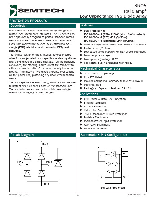
SR05
Mechanical Characteristics
JEDEC SOT-143 package UL 497B listed Molding compound flammability rating: UL 94V-0 Marking : R05 Packaging : Tape and Reel per EIA 481
0
25
50
75
100
125
150
Ambient Temperature - TA (oC)
Pulse Waveform
110 100 90 80 Percent of IPP 70 60 50 40 30 20 10 0 0 5 10 15 Time (µs) 20 25 30 td = IPP/2 e
10 Peak Pulse Power - PPk (kW)
Power Derating Curve
1IP 90 80 70 60 50 40 30 20 10 0
1
0.1
RClamp0504S.TCT中文资料
PROTECTION PRODUCTS - RailClamp Description
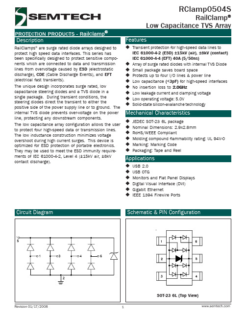
RailClamps are surge rated diode arrays designed to protect high speed data interfaces. This series has been specifically designed to protect sensitive components which are connected to data and transmission lines from overvoltage caused by ESD (electrostatic discharge), CDE (Cable Discharge Events), and EFT (electrical fast transients). The unique design incorporates surge rated, low capacitance steering diodes and a TVS diode in a single package. During transient conditions, the steering diodes direct the transient to either the positive side of the power supply line or to ground. The internal TVS diode prevents over-voltage on the power line, protecting any downstream components. The low capacitance array configuration allows the user to protect four high-speed data or transmission lines. The low inductance construction minimizes voltage overshoot during high current surges. This device is optimized for ESD protection of portable electronics. They may be used to meet the ESD immunity requirements of IEC 61000-4-2, Level 4 (±15kV air, ±8kV contact discharge).
RailClamps are surge rated diode arrays designed to protect high speed data interfaces. This series has been specifically designed to protect sensitive components which are connected to data and transmission lines from overvoltage caused by ESD (electrostatic discharge), CDE (Cable Discharge Events), and EFT (electrical fast transients). The unique design incorporates surge rated, low capacitance steering diodes and a TVS diode in a single package. During transient conditions, the steering diodes direct the transient to either the positive side of the power supply line or to ground. The internal TVS diode prevents over-voltage on the power line, protecting any downstream components. The low capacitance array configuration allows the user to protect four high-speed data or transmission lines. The low inductance construction minimizes voltage overshoot during high current surges. This device is optimized for ESD protection of portable electronics. They may be used to meet the ESD immunity requirements of IEC 61000-4-2, Level 4 (±15kV air, ±8kV contact discharge).
RCLAMP0821P中文资料

Mechanical Characteristics
SLP1006P2 package Molding compound flammability rating: UL 94V-0 Marking: Marking code Packaging : Tape and Reel Lead Finish: NiPdAu RoHS/WEEE Compliant
I/O Line
RClamp0821P
RClamp0821P Spice Model
Table 1 - RClamp0821P Spice Parameters
Parameter
Unit
D1 (LCRD) D2 (LCRD)
IS
Amp
1.0E-20
1.0E-20
BV
Vlt
0.7
元器件交易网
PROTECTION PRODUCTS Applications Information
Device Connection Options
These low capacitance TVS diodes are designed to provide common mode protection for one high-speed line or differential protection for one line pair. The device is bidirectional and may be used on lines where the signal polarity is positive and negative.
1.8 GHz
1
2 34
3: .00910 dB 2.5 GHz
4: -.11980 dB 2.7 GHz
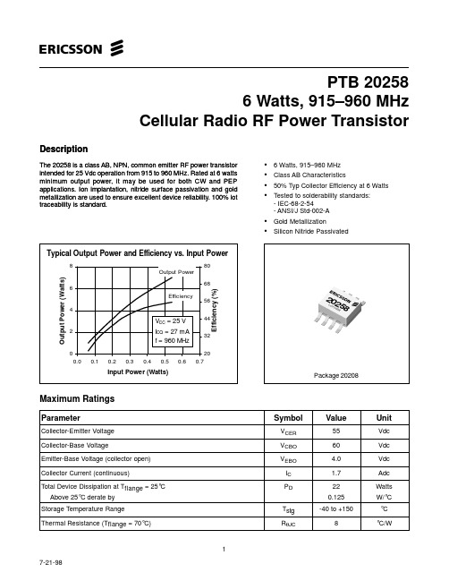
PTB20258资料
0
20
0.0 0.1 0.2 0.3 0.4 0.5 0.6 0.7
Input Power (Watts)
Maximum Ratings
Parameter
Collector-Emitter Voltage Collector-Base Voltage Emitter-Base Voltage (collector open) Collector Current (continuous) Total Device Dissipation at Tflange = 25°C
ICQ = 27 mA
12
10
ICQ = 7 mA
8
ICQ = 14 mA VCC = 25V
f = 960 MHz
6
0.10
1.00
Output Power (W)
10.00
Impedance Data
(VCC = 25 Vdc, Pout = 6 W, ICQ = 27 mA)
Z Source
Z Load
RF Specifications (100% Tested)
Characteristic
Gain (VCC = 25 Vdc, Pout = 6 W, ICQ = 27 mA, f = 960 MHz)
Collector Efficiency (VCC = 25 Vdc, Pout = 6 W, ICQ = 27 mA, f = 960 MHz)
(as measured in a broadband circuit)
13
VCC = 25 V
12
ICQ = 27 mA
POUT = 6 W
11
10
RCLAMP0522P中文资料
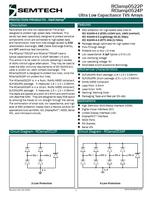
Applications
High Definition Multi-Media Interface (HDMI) Digital Visual Interface (DVI) Unified Display Interface (UDI) DisplayPortTM Interface MDDI Ports PCI Express Serial ATA
RClamp0522P RClamp0524P
PRELIMINARY
Power Derating Curve
110 100 90 80 70 60 50 40 30 20 10 0
PROTECTION PRODUCTS Typical Characteristics
Non-Repetitive Peak Pulse Power vs. Pulse Time
Pin 1
Pin 2
Pin 1
Pin 2
Pin 4
Pin 5
3, 4
3, 8
Circuit Diagram
Circuit Diagram
Ordering Information
Part Number RClamp0522P.TCT RClamp0524P.TCT Number of Lines Qty per Reel Reel Size 7 Inch 7 Inch
PRELIMINARY
RClamp0522P RClamp0524P
RClamp0524P
10 9 8 7 6
1
Pin 1-2 5-6 3-4
2
3
Identification Input Lines Output Lines (No Internal Connection) Ground Pin
rclamp0502b工作原理
rClamp0502B是一款常见的电阻器,其工作原理是基于欧姆定律。
当电流流过电阻器时,电阻器会对其产生一定的电压降,同时也会产生一定的功率损耗。
rClamp0502B的电阻值可以通过调整电阻丝的直径或长度来改变,从而控制通过电阻器的电流大小,进而实现对电压或电流的限制作用。
具体来说,当电源为rClamp0502B提供电流时,电阻器会产生电压降,该电压降被用来调节通过电路中的电流。
如果电路中的电流超过设定的阈值,电阻器将通过消耗更多的功率来降低电流,从而起到保护电路的作用。
这种保护机制可以防止电路过载,避免电路中的元器件受到损坏。
除了限制电流的作用外,rClamp0502B还可以用作分压器。
当两个电阻器串联时,它们的电压将按照电阻值的大小进行分配。
因此,如果一个电阻器的电阻值较大,那么它将会承受更多的电压,而另一个电阻器则承受较小的电压。
这种分压方式可以用于调节电路中的电压,以满足电路中其他元器件的需求。
此外,rClamp0502B还具有一些其他的特点和优点。
首先,它是一种常见的电子元件,价格相对较低,易于购买和更换。
其次,它具有较高的稳定性和可靠性,可以长时间稳定工作而不易损坏。
最后,rClamp0502B的体积较小,易于集成到电路板中,有利于提高电路的可靠性和便携性。
总之,rClamp0502B的工作原理是基于欧姆定律,通过限制电流或用作分压器来保护电路中的元器件。
它是一种常见的电子元件,具有较高的稳定性和可靠性,易于购买和更换,适用于各种电路中的电压和电流调节需求。
在实际应用中,rClamp0502B通常与其他电子元件配合使用,以实现更复杂的功能和系统优化。
RCLAMP0524J.TCT中文资料

Cj
Conditions
Any I/O pin to ground
It = 1mA Any I/O pin to ground
VRWM = 5V, T=25°C Any I/O pin to ground
IPP = 1A, tp = 8/20μs Any I/O pin to ground
V = 0V, f = 1MHz R
Dimensions
Circuit Diagram
2.70 0.40
12
1.00
0.60 0.20
0.50
0.58
Pin 1
Pin 2
Pin 3
Pin 4
GND
Nominal Dimensions in mm
Revision 02/05/2008
1
4-Line Protection
3 2: -0.062 dB
1
2
1.8 GHz
3: -0.1087 dB 2.5 GHz
100 MHz
13 GHz GHz
STOP 3000.000000 MHz
RClamp0524J
PRELIMINARY
Insertion Loss S21 - I/O to GND
CH1 S21 LOG 6 dB / REF 0 dB
Mechanical Characteristics
SLP2710P8 8-pin package (2.7 x 1.0 x 0.58mm) RoHS/WEEE Compliant Lead Pitch: 0.5mm Lead finish: NiPdAu Marking: Marking Code Packaging: Tape and Reel per EIA 481
RCLamp0508M.TBT资料

CJ(VR) / C J(V R=0)
1.8 1.6 1.4 1.2 1 0.8 0.6 0.4 0.2 0 0 1 2 3 4 f = 1 MHz 5
2.00
4.00
6.00
8.00
10.00
12.00
Forward Current - IF (A)
Reverse Voltage - VR (V)
Power Derating Curve
Peak Pulse Power - PPP (kW)
1
0.1
0.01 0.1 1 10 Pulse Duration - tp (µs) 100 1000
0
25
50
75
100
125
150
Ambient Temperature - TA (oC)
Pulse Waveform
30.00 Clamping Voltage -Vc (V) 25.00 20.00 15.00 10.00 5.00 0.00 0.00 Waveform Parameters: tr = 8µs td = 20µs 2.00 4.00 6.00 8.00 10.00 12.00
Percent of I
CH1 S21 LOG 20 dB/ REF 0 dB
START
.030 000 MHz
STOP 3 RT
.030 000 MHz
STOP 3 000. 000 000 MHz
2008 Semtech Corp.
4
RClamp0508M
e-t
Peak Pulse Current - Ipp (A)
Forward Voltage vs. Forward Current
- 1、下载文档前请自行甄别文档内容的完整性,平台不提供额外的编辑、内容补充、找答案等附加服务。
- 2、"仅部分预览"的文档,不可在线预览部分如存在完整性等问题,可反馈申请退款(可完整预览的文档不适用该条件!)。
- 3、如文档侵犯您的权益,请联系客服反馈,我们会尽快为您处理(人工客服工作时间:9:00-18:30)。
1.4 1.2
1 0.8 0.6 0.4 0.2
0 0
f = 1 MHz
1
2
3
4
5
Reverse Voltage - VR (V)
Normalized Capacitance - Cj
1.2 1
0.8 0.6 0.4 0.2
0
2005 Semtech Corp.
3
f = 1 MHz
1
2
3
4
5
Reverse Voltage - VR (V)
2: .02010 dB 1.8 GHz
3: -.08180 dB 2.5 GHz
3
1
2
-12 dB -18 dB
-24 dB
-30 dB
-36 dB
1 MHz
START. 030 MHz
10 MHz
100 MHz
13 GHz GHz
STOP 3000.000000 MHz
ESD Response (8kV Contact per IEC 61000-4-2)
Applications
High-Definition Multimedia Interface (HDMI) Mobile Display Digital Interface (MDDI) RF/Antenna Circuits USB 2.0 & Firewire Ports GaAs Photodetector Protection HBT Power Amp Protection Infiniband Transceiver Protection
25
20
15
10
5
0 0
Waveform Parameters:
tr = 8µs td = 20µs
1
2
3
4
5
6
Peak Pulse Current - IPP (A)
Normalized Capacitance vs. Reverse Voltage Pin 1 or Pin 2 to Pin 3
ESD Response (4kV Contact per IEC 61000-4-2)
RClamp0502B
Insertion Loss S21 (Pin 1 or Pin 2 to Pin 3)
CH1 S21 LOG 6 dB / REF 0 dB
0 dB -6 dB
1: .00460 dB 900 MHz
元器件交易网
PROTECTION PRODUCTS Absolute Maximum Rating
Rating Peak Pulse Power (tp = 8/20µs) Peak Pulse Current (tp = 8/20µs) ESD per IEC 61000-4-2 (Air) ESD per IEC 61000-4-2 (Contact) Operating Temperature Storage Temperature
Non-Repetitive Peak Pulse Power vs. Pulse Time
10
Peak Pulse Power - PPP (kW)
1
0.1
Clamping Voltage - VC (V)
0.01 0.1
1
10
100
Pulse Duration - tp (µs)
1000
Clamping Voltage vs. Peak Pulse Current Pin 1 to Pin 2
-12 dB -18 dB
-24 dB
-30 dB
-36 dB
1 MHz
START. 030 MHz
10 MHz
1: .03430 dB 900 MHz
2: .07870 dB 1.8 GHz
3: .28040 dB 2.5 GHz
3
1
2
100 MHz
13 GHz GHz
STOP 3000.000000 MHz
Minimum 6
Typical
Maximum 5
Units V
Vቤተ መጻሕፍቲ ባይዱ
1
µA
15
V
22
V
25
V
0.60
0.9
pF
1.2
pF
2005 Semtech Corp.
2
元器件交易网
RClamp0502B
PROTECTION PRODUCTS Typical Characteristics
% of Rated Power or IPP
Clamping Voltage - VC (V)
Power Derating Curve
110 100
90 80 70 60 50 40 30 20 10
0 0
25
50
75
100
125
150
Ambient Temperature - TA (oC)
Clamping Voltage vs. Peak Pulse Current Pin 1 or Pin 2 to Pin 3
RClamp0502B
Ultra-Low Capacitance TVS for ESD and CDE Protection
Features
Transient protection for high-speed data lines to IEC 61000-4-2 (ESD) ±15kV (air), ±8kV (contact) IEC 61000-4-4 (EFT) 40A (5/50ns)
20
18
16
14
12
10
8
6
Waveform
4
Parameters: tr = 8µs
2
td = 20µs
0
0
1
2
3
4
5
6
Peak Pulse Current - IPP (A)
Normalized Capacitance vs. Reverse Voltage Pin 1 to Pin 2
NormalizedCapacitance - Cj
元器件交易网
PROTECTION PRODUCTS - RailClamp Description
RailClamps are ultra low capacitance TVS arrays designed to protect high speed data interfaces. This series has been specifically designed to protect sensitive components which are connected to high-speed data and transmission lines from overvoltage caused by ESD (electrostatic discharge), CDE (Cable Discharge Events), and EFT (electrical fast transients). The RClampTM0502B has a typical capacitance of only 0.50pF (pin 1 to 2). This means it can be used on circuits operating in excess of 3GHz without signal attenuation. They may be used to meet the ESD immunity requirements of IEC 61000-4-2, Level 4 (±15kV air, ±8kV contact discharge). Each device can be configured to protect 1 bidirectional line or two unidirectional lines. These devices are in a small SC-75 (SOT-523) package and feature a lead-free, matte tin finish. They are compatible with both lead free and SnPb assembly techniques. They are designed for use in applications where board space is at a premium. The combination of small size, low capacitance, and high level of ESD protection makes them a flexible solution for applications such as HDMI, MDDI, antenna circuits, Automatic Test Equipment, USB 2.0, and Infiniband circuits.
IPP = 1A, tp = 8/20µs Pin 1 to Pin 2
IPP = 5A, tp = 8/20µs Pin 1 or Pin 2 to Pin 3
IPP = 5A, tp = 8/20µs Pin 1 to Pin 2
VR = 0V, f = 1MHz Pin 1 to Pin 2
VR = 0V, f = 1MHz Pin 1 or Pin 2 to Pin 3
元器件交易网
PROTECTION PRODUCTS Typical Characteristics