MMSZ5264中文资料
MMSZ5242中文资料

Cathode Mark
.152 (3.85) .140 (3.55) .112 (2.85) .100 (2.55)
Top View
max. .004 (0.1)
max. .053 (1.35)
min. .010 (0.25)
max. .006 (0.15)
.067 (1.70) .055 (1.40)
50 25 15 10 5.0 5.0 5.0 5.0 5.0 5.0 3.0 3.0 3.0 3.0 3.0 3.0 2.0 1.0 0.5 0.1 0.1 0.1 0.1 0.1 0.1 0.1 0.1 0.1 0.1 0.1 0.1 0.1 0.1 0.1 0.1 0.1 0.1 0.1 0.1 0.1 0.1 0.1 0.1
1.0 1.0 1.0 1.0 1.0 2.0 2.0 3.0 3.5 4.0 5.0 6.0 6.5 6.5 7.0 8.0 8.4 9.1 9.9 10 11 12 13 14 14 15 17 18 19 21 21 23 25 27 30 33 36 39 43 46 47 52 56
NOTES: (1) The Zener Impedance is derived from the 1kHz AC voltage which results when an AC current having an RMS value equal to 10% of the Zener current (IZT or IZK) is superimposed on IZT or IZK. Zener Impedance is measured at two points to insure a sharp knee on the breakdown curve and to eliminate unstable units. (2) Measured with device junction in thermal equilibrium.
MMSZ5265BT1中文资料

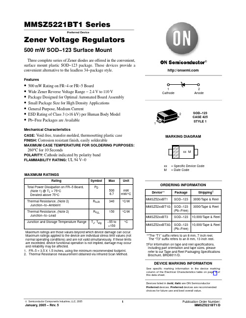
MMSZ5221BT1 SeriesPreferred DeviceZener Voltage Regulators 500 mW SOD−123 Surface MountThree complete series of Zener diodes are offered in the convenient, surface mount plastic SOD−123 package. These devices provide a convenient alternative to the leadless 34−package style.Features•500 mW Rating on FR−4 or FR−5 Board•Wide Zener Reverse V oltage Range − 2.4 V to 110 V •Package Designed for Optimal Automated Board Assembly •Small Package Size for High Density Applications •General Purpose, Medium Current•ESD Rating of Class 3 (>16 kV) per Human Body Model•Pb−Free Packages are AvailableMechanical CharacteristicsCASE:V oid-free, transfer-molded, thermosetting plastic case FINISH:Corrosion resistant finish, easily solderableMAXIMUM CASE TEMPERATURE FOR SOLDERING PURPOSES: 260°C for 10 SecondsPOLARITY:Cathode indicated by polarity band FLAMMABILITY RATING:UL 94 V−0MAXIMUM RATINGSMaximum ratings are those values beyond which device damage can occur. Maximum ratings applied to the device are individual stress limit values (not normal operating conditions) and are not valid simultaneously. If these limits are exceeded, device functional operation is not implied, damage may occur and reliability may be affected.1.FR−5 = 3.5 X 1.5 inches, using the minimum recommended footprint.2.Thermal Resistance measurement obtained via infrared Scan Method.See specific marking information in the device marking column of the Electrical Characteristics table on page 3 of this data sheet.DEVICE MARKING INFORMATIONDevices listed in bold, italic are ON Semiconductor Preferred devices. Preferred devices are recommended choices for future use and best overall value.ELECTRICAL CHARACTERISTICS (T A = 25°C unlessotherwise noted, V= 0.95 V Max. @ I = 10 mA)4.Nominal Zener voltage is measured with the device junction in thermal equilibrium at T L = 30°C $1°C.5.Z ZT and Z ZK are measured by dividing the AC voltage drop across the device by the ac current applied.The specified limits are for I Z(AC) = 0.1 I Z(dc) with the AC frequency = 1 KHz.V Z , NOMINAL ZENER VOLTAGE (V)−1012345678Figure 1. Temperature Coefficients (Temperature Range −55°C to +150°C)100101V Z , NOMINAL ZENER VOLTAGE (V)Figure 2. Temperature Coefficients (Temperature Range −55°C to +150°C)1.21.00.80.60.40.20T, TEMPERATURE (°C)Figure 3. Steady State Power Derating PW, PULSE WIDTH (ms)Figure 4. Maximum Nonrepetitive Surge Power1000100101V Z , NOMINAL ZENER VOLTAGEFigure 5. Effect of Zener Voltage onZener Impedance100101V F , FORWARD VOLTAGE (V)Figure 6. Typical Forward Voltage1000100101q V Z , T E M P E R A T U R E C O E F F I C I E N T (m V /°C )q V Z , T E M P E R A T U R E C O E F F I C I E N T (m V /°C )P p k , P E A K S U R G E P O W E R (W A T T S )Z Z T , D Y N A M I C I M P E D A N C E (W )I F , F O R W A R D C U R R E N T (m A )C , C A P A C I T A N C E (p F )V Z , NOMINAL ZENER VOLTAGE (V)Figure 7. Typical Capacitance 1000100101V Z , ZENER VOLTAGE (V)1001010.10.01V Z , ZENER VOLTAGE (V)1001010.10.01V Z , NOMINAL ZENER VOLTAGE (V)Figure 8. Typical Leakage CurrentFigure 9. Zener Voltage versus Zener Current(V Z Up to 12 V)Figure 10. Zener Voltage versus Zener Current(12 V to 91 V)I R , L E A K A G E C U R R E N T (m A )I Z , Z E N E R C U R R E N T (m A )I Z , Z E N E R C U R R E N T (m A )PACKAGE DIMENSIONSSOD−123CASE 425−04ISSUE Cǒmm inchesǓSCALE 10:1*For additional information on our Pb−Free strategy and solderingdetails, please download the ON Semiconductor Soldering and Mounting Techniques Reference Manual, SOLDERRM/D.SOLDERING FOOTPRINT*ON Semiconductor and are registered trademarks of Semiconductor Components Industries, LLC (SCILLC). SCILLC reserves the right to make changes without further notice to any products herein. SCILLC makes no warranty, representation or guarantee regarding the suitability of its products for any particular purpose, nor does SCILLC assume any liability arising out of the application or use of any product or circuit, and specifically disclaims any and all liability, including without limitation special, consequential or incidental damages.“Typical” parameters which may be provided in SCILLC data sheets and/or specifications can and do vary in different applications and actual performance may vary over time. All operating parameters, including “Typicals” must be validated for each customer application by customer’s technical experts. SCILLC does not convey any license under its patent rights nor the rights of others. SCILLC products are not designed, intended, or authorized for use as components in systems intended for surgical implant into the body, or other applications intended to support or sustain life, or for any other application in which the failure of the SCILLC product could create a situation where personal injury or death may occur. Should Buyer purchase or use SCILLC products for any such unintended or unauthorized application, Buyer shall indemnify and hold SCILLC and its officers, employees, subsidiaries, affiliates,and distributors harmless against all claims, costs, damages, and expenses, and reasonable attorney fees arising out of, directly or indirectly, any claim of personal injury or death associated with such unintended or unauthorized use, even if such claim alleges that SCILLC was negligent regarding the design or manufacture of the part. SCILLC is an Equal Opportunity/Affirmative Action Employer. This literature is subject to all applicable copyright laws and is not for resale in any manner.PUBLICATION ORDERING INFORMATION。
5264型连接器规格书-浙江乐深电子

损伤,颜色一致,标志清晰。
(可用 3~5 倍放大镜观察)
Байду номын сангаас
符合产品图示
游标卡尺测量、投影仪测量
-3-
3 3.3 互换性
相同型号规格的连接器能通用互 常规使用条件 换。
4 3.4
将连接器固定于推拉力计上,将针座
插入力 拔出力
插入力≤15N×接触件数 拔出力≥2N×接触数数
以 1-5mm/s 的速度沿轴线方向插入 孔座,插入时的力为插入力,分离时 的力为拔出力。
不露出底金属、无严重锈蚀。 (预镀材料允许冲切面有轻度腐 蚀)
连接器在插合状态下进行测试: 温度:35±2℃ 浓度:(重量比)5% 暴露 48 小时后用清水冲洗,自然干 燥后测试。
焊接端应容易被熔融焊料润湿, 沾锡面积应占浸入面积的 90%以 上。 实验结束后,在正常条件下恢复 1h,连接器无变形、损伤及跳针 现象。 连接器使用材料符合 UL94V-0 级 要求。
温度:235±5℃ 时间:2±0.05s
温度:260±5℃ 时间:5±1s
参照 UL94V(垂直燃烧试验法)或 提供制造商材料合格证明。
4. 逐批交收检验 4.1
序号
项目
1
外观
2
尺寸
3
插拔力
4
接触电阻
5
绝缘电阻
6
耐电压
7
可焊性
8
耐焊接热
试验条件及方法 3.1 符合产品图示 3.4 3.8 3.9 3.10 3.16 3.17
目视检查可用35倍放大镜观察32结构尺寸符合产品图示游标卡尺测量投影仪测量5264接触件数接触件类型引出端形状数字表示a表示针座y表示孔座w表示弯式不注表示立式33互换性相同型号规格的连接器能通用互34插入力拔出力插入力15n接触件数拔出力2n接触数数将连接器固定于推拉力计上将针座15mms的速度沿轴线方向插入孔座插入时的力为插入力分离时的力为拔出力
MMSZ5254B中文资料

Antistatic Cover Tape
F63TNR Label
Static Dissipative Embossed Carrier Tape
Cathode
SOD123 Packaging Information Packaging Option Packaging type Qty per Reel/Tube/Bag Reel Size Box Dimension (mm) Max qty per Box Weight per unit (gm) Weight per Reel (kg) Note/Comments Standard (no flow code) TNR 3,000 7" Dia 184x187x47 9,000 0.01 0.123 L99Z TNR 3,000 7" Dia 184x187x47 9,000 0.01 0.123 No marking required D87Z TNR 10,000 13" 343x343x64 30,000 0.01 0.420
Component Rotation
W1 Measured at Hub
Dim A Max
Dim A max
Dim N
See detail AA
7" Diameter Option
B Min Dim C See detail AA W3
Dim D min
13" Diameter Option
W2 max Measured at Hub DETAIL AA
Dimensions are in inches and millimeters
Tape Size
8mm
Reel Option
MMSZ5256资料

Cathode Mark
.152 (3.85) .140 (3.55) .112 (2.85) .100 (2.55)
Top View
max. .004 (0.1)
max. .053 (1.35)
min. .010 (0.25)
max. .006 (0.15)
.067 (1.70) .055 (1.40)
1/20/99
元器件交易网
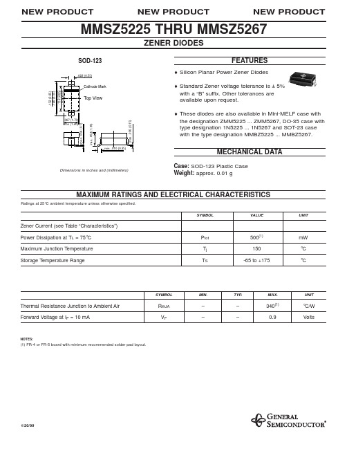
MMSZ5225 THRU MMSZ5267
ELECTRICAL CHARACTERISTICS
Ratings at 25°C ambient temperature unless otherwise specified.
Type
Marking Code
1.0 1.0 1.0 1.0 1.0 2.0 2.0 3.0 3.5 4.0 5.0 6.0 6.5 6.5 7.0 8.0 8.4 9.1 9.9 10 11 12 13 14 14 15 17 18 19 21 21 23 25 27 30 33 36 39 43 46 47 52 56
NOTES: (1) The Zener Impedance is derived from the 1kHz AC voltage which results when an AC current having an RMS value equal to 10% of the Zener current (IZT or IZK) is superimposed on IZT or IZK. Zener Impedance is measured at two points to insure a sharp knee on the breakdown curve and to eliminate unstable units. (2) Measured with device junction in thermal equilibrium.
MMSZ5231中文资料

NEW PRODUCT
NEW PRODUCT
MMSZ5225 THRU MMSZ5267
ZENER DIODES
SOD-123
.022 (0.55)
FEATURES
♦ Silicon Planar Power Zener Diodes ♦ Standard Zener voltage tolerance is ± 5% with a “B” suffix. Other tolerances are available upon request. ♦ These diodes are also available in Mini-MELF case with the designation ZMM5225 ... ZMM5267, DO-35 case with type designation 1N5225 ... 1N5267 and SOT-23 case with the type designation MMBZ5225 ... MMBZ5267.
(%/K)
IR (µA)
Test Voltage VR (V)
MMSZ5225 MMSZ5226 MMSZ5227 MMSZ5228 MMSZ5229 MMSZ5230 MMSZ5231 MMSZ5232 MMSZ5233 MMSZ5234 MMSZ5235 MMSZ5236 MMSZ5237 MMSZ5238 MMSZ5239 MMSZ5240 MMSZ5241 MMSZ5242 MMSZ5243 MMSZ5244 MMSZ5245 MMSZ5246 MMSZ5247 MMSZ5248 MMSZ5249 MMSZ5250 MMSZ5251 MMSZ5252 MMSZ5253 MMSZ5254 MMSZ5255 MMSZ5256 MMSZ5257 MMSZ5258 MMSZ5259 MMSZ5260 MMSZ5261 MMSZ5262 MMSZ5263 MMSZ5264 MMSZ5265 MMSZ5266 MMSZ5267
MMSZ5232BT1中文资料
MMSZ5221BT1 SeriesPreferred DeviceZener Voltage Regulators 500 mW SOD−123 Surface MountThree complete series of Zener diodes are offered in the convenient, surface mount plastic SOD−123 package. These devices provide a convenient alternative to the leadless 34−package style.Features•500 mW Rating on FR−4 or FR−5 Board•Wide Zener Reverse V oltage Range − 2.4 V to 110 V •Package Designed for Optimal Automated Board Assembly •Small Package Size for High Density Applications •General Purpose, Medium Current•ESD Rating of Class 3 (>16 kV) per Human Body Model•Pb−Free Packages are AvailableMechanical CharacteristicsCASE:V oid-free, transfer-molded, thermosetting plastic case FINISH:Corrosion resistant finish, easily solderableMAXIMUM CASE TEMPERATURE FOR SOLDERING PURPOSES: 260°C for 10 SecondsPOLARITY:Cathode indicated by polarity band FLAMMABILITY RATING:UL 94 V−0MAXIMUM RATINGSMaximum ratings are those values beyond which device damage can occur. Maximum ratings applied to the device are individual stress limit values (not normal operating conditions) and are not valid simultaneously. If these limits are exceeded, device functional operation is not implied, damage may occur and reliability may be affected.1.FR−5 = 3.5 X 1.5 inches, using the minimum recommended footprint.2.Thermal Resistance measurement obtained via infrared Scan Method.See specific marking information in the device marking column of the Electrical Characteristics table on page 3 of this data sheet.DEVICE MARKING INFORMATIONDevices listed in bold, italic are ON Semiconductor Preferred devices. Preferred devices are recommended choices for future use and best overall value.ELECTRICAL CHARACTERISTICS (T A = 25°C unlessotherwise noted, V= 0.95 V Max. @ I = 10 mA)4.Nominal Zener voltage is measured with the device junction in thermal equilibrium at T L = 30°C $1°C.5.Z ZT and Z ZK are measured by dividing the AC voltage drop across the device by the ac current applied.The specified limits are for I Z(AC) = 0.1 I Z(dc) with the AC frequency = 1 KHz.V Z , NOMINAL ZENER VOLTAGE (V)−1012345678Figure 1. Temperature Coefficients (Temperature Range −55°C to +150°C)100101V Z , NOMINAL ZENER VOLTAGE (V)Figure 2. Temperature Coefficients (Temperature Range −55°C to +150°C)1.21.00.80.60.40.20T, TEMPERATURE (°C)Figure 3. Steady State Power Derating PW, PULSE WIDTH (ms)Figure 4. Maximum Nonrepetitive Surge Power1000100101V Z , NOMINAL ZENER VOLTAGEFigure 5. Effect of Zener Voltage onZener Impedance100101V F , FORWARD VOLTAGE (V)Figure 6. Typical Forward Voltage1000100101q V Z , T E M P E R A T U R E C O E F F I C I E N T (m V /°C )q V Z , T E M P E R A T U R E C O E F F I C I E N T (m V /°C )P p k , P E A K S U R G E P O W E R (W A T T S )Z Z T , D Y N A M I C I M P E D A N C E (W )I F , F O R W A R D C U R R E N T (m A )C , C A P A C I T A N C E (p F )V Z , NOMINAL ZENER VOLTAGE (V)Figure 7. Typical Capacitance 1000100101V Z , ZENER VOLTAGE (V)1001010.10.01V Z , ZENER VOLTAGE (V)1001010.10.01V Z , NOMINAL ZENER VOLTAGE (V)Figure 8. Typical Leakage CurrentFigure 9. Zener Voltage versus Zener Current(V Z Up to 12 V)Figure 10. Zener Voltage versus Zener Current(12 V to 91 V)I R , L E A K A G E C U R R E N T (m A )I Z , Z E N E R C U R R E N T (m A )I Z , Z E N E R C U R R E N T (m A )PACKAGE DIMENSIONSSOD−123CASE 425−04ISSUE Cǒmm inchesǓSCALE 10:1*For additional information on our Pb−Free strategy and solderingdetails, please download the ON Semiconductor Soldering and Mounting Techniques Reference Manual, SOLDERRM/D.SOLDERING FOOTPRINT*ON Semiconductor and are registered trademarks of Semiconductor Components Industries, LLC (SCILLC). SCILLC reserves the right to make changes without further notice to any products herein. SCILLC makes no warranty, representation or guarantee regarding the suitability of its products for any particular purpose, nor does SCILLC assume any liability arising out of the application or use of any product or circuit, and specifically disclaims any and all liability, including without limitation special, consequential or incidental damages.“Typical” parameters which may be provided in SCILLC data sheets and/or specifications can and do vary in different applications and actual performance may vary over time. All operating parameters, including “Typicals” must be validated for each customer application by customer’s technical experts. SCILLC does not convey any license under its patent rights nor the rights of others. SCILLC products are not designed, intended, or authorized for use as components in systems intended for surgical implant into the body, or other applications intended to support or sustain life, or for any other application in which the failure of the SCILLC product could create a situation where personal injury or death may occur. Should Buyer purchase or use SCILLC products for any such unintended or unauthorized application, Buyer shall indemnify and hold SCILLC and its officers, employees, subsidiaries, affiliates,and distributors harmless against all claims, costs, damages, and expenses, and reasonable attorney fees arising out of, directly or indirectly, any claim of personal injury or death associated with such unintended or unauthorized use, even if such claim alleges that SCILLC was negligent regarding the design or manufacture of the part. SCILLC is an Equal Opportunity/Affirmative Action Employer. This literature is subject to all applicable copyright laws and is not for resale in any manner.PUBLICATION ORDERING INFORMATION。
MMSZ5240中文资料
1/20/99
元器件交易网
MMSZ5225 THRU MMSZ5267
ELECTRICAL CHARACTERISTICS
Ratings at 25°C ambient temperature unless otherwise specified.
Type
Marking Code
MECHANICAL DATA
Case: SOD-123 Plastic Case Weight: approx. 0.01 g
Dimensions in inches and (millimeters)
MAXIMUM RATINGS AND ELECTRICAL CHARACTERISTICS
Ratings at 25°C ambient temperature unless otherwise specified.
-0.075 -0.070 -0.065 -0.060 -0.055 ±0.030 ±0.030 +0.038 +0.038 +0.045 +0.050 +0.058 +0.062 +0.065 +0.068 +0.075 +0.076 +0.077 +0.079 +0.082 +0.082 +0.083 +0.084 +0.085 +0.086 +0.086 +0.087 +0.087 +0.089 +0.090 +0.091 +0.091 +0.092 +0.093 +0.094 +0.095 +0.095 +0.096 +0.096 +0.097 +0.097 +0.097 +0.098
- 1、下载文档前请自行甄别文档内容的完整性,平台不提供额外的编辑、内容补充、找答案等附加服务。
- 2、"仅部分预览"的文档,不可在线预览部分如存在完整性等问题,可反馈申请退款(可完整预览的文档不适用该条件!)。
- 3、如文档侵犯您的权益,请联系客服反馈,我们会尽快为您处理(人工客服工作时间:9:00-18:30)。
1/20/99
元器件交易网
MMSZ5225 THRU MMSZ5267
ELECTRICAL CHARACTERISTICS
Ratings at 25°C ambient temperature unless otherwise specified.
Type
Marking Code
Nominal Zener voltage(3) at IZT VZ (V)
Maximum Zener impedance(1) Test current IZT (mA) at IZT ZZT (Ω) at IZK = 0.25 mA ZZK (Ω)
Maximum Reverse Leakage Current Typical Temperture Coefficient αvz
SYMBOL
VALUE
UNIT
Zener Current (see Table “Characteristics”) Power Dissipation at TL = 75°C Maximum Junction Temperature Storage Temperature Range Ptot Tj TS 500(1) 150 -65 to +175 mW °C °C
30 28 24 23 22 19 17 11 7 7 5 6 8 8 10 17 22 30 13 15 16 17 19 21 23 25 29 33 35 41 44 49 58 70 80 93 105 125 150 170 185 230 270
1600 1600 1700 1900 2000 1900 1600 1600 1600 1000 750 500 500 600 600 600 600 600 600 600 600 600 600 600 600 600 600 600 600 600 600 600 700 700 800 900 1000 1100 1300 1400 1400 1600 1700
50 25 15 10 5.0 5.0 5.0 5.0 5.0 5.0 3.0 3.0 3.0 3.0 3.0 3.0 2.0 1.0 0.5 0.1 0.1 0.1 0.1 0.1 0.1 0.1 0.1 0.1 0.1 0.1 0.1 0.1 0.1 0.1 0.1 0.1 0.1 0.1 0.1 0.1 0.1 0.1 0.1
元器件交易网 NEW PRODUCT
NEW PRODUCT
NEW PRODUCT
MMSZ5225 THRU MMSZ5267
ZENER DIODES
SOD-123
.022 (0.55)
FEATURES
♦ Silicon Planar Power Zener Diodes ♦ Standard Zener voltage tolerance is ± 5% with a “B” suffix. Other tolerances are available upon request. ♦ These diodes are also available in Mini-MELF case with the designation ZMM5225 ... ZMM5267, DO-35 case with type designation 1N5225 ... 1N5267 and SOT-23 case with the type designation MMBZ5225 ... MMBZ5267.
SYMBOL
Resistance Junction to Ambient Air Forward Voltage at IF = 10 mA
RΘJA VF
– –
– –
340(1) 0.9
°C/W Volts
NOTES:
(1) FR-4 or FR-5 board with minimum recommended solder pad layout.
20 20 20 20 20 20 20 20 20 20 20 20 20 20 20 20 20 20 9.5 9.0 8.5 7.8 7.4 7.0 6.6 6.2 5.6 5.2 5.0 4.6 4.5 4.2 3.8 3.4 3.2 3.0 2.7 2.5 2.2 2.1 2.0 1.8 1.7
1.0 1.0 1.0 1.0 1.0 2.0 2.0 3.0 3.5 4.0 5.0 6.0 6.5 6.5 7.0 8.0 8.4 9.1 9.9 10 11 12 13 14 14 15 17 18 19 21 21 23 25 27 30 33 36 39 43 46 47 52 56
NOTES: (1) The Zener Impedance is derived from the 1kHz AC voltage which results when an AC current having an RMS value equal to 10% of the Zener current (IZT or IZK) is superimposed on IZT or IZK. Zener Impedance is measured at two points to insure a sharp knee on the breakdown curve and to eliminate unstable units. (2) Measured with device junction in thermal equilibrium.
C5 D1 D2 D3 D4 D5 E1 E2 E3 E4 E5 F1 F2 F3 F4 F5 H1 H2 H3 H4 H5 J1 J2 J3 J4 J5 K1 K2 K3 K4 K5 M1 M2 M3 M4 M5 N1 N2 N3 N4 N5 P1 P2
3.0 3.3 3.6 3.9 4.3 4.7 5.1 5.6 6.0 6.2 6.8 7.5 8.2 8.7 9.1 10 11 12 13 14 15 16 17 18 19 20 22 24 25 27 28 30 33 36 39 43 47 51 56 60 62 68 75
-0.075 -0.070 -0.065 -0.060 -0.055 ±0.030 ±0.030 +0.038 +0.038 +0.045 +0.050 +0.058 +0.062 +0.065 +0.068 +0.075 +0.076 +0.077 +0.079 +0.082 +0.082 +0.083 +0.084 +0.085 +0.086 +0.086 +0.087 +0.087 +0.089 +0.090 +0.091 +0.091 +0.092 +0.093 +0.094 +0.095 +0.095 +0.096 +0.096 +0.097 +0.097 +0.097 +0.098
Cathode Mark
.152 (3.85) .140 (3.55) .112 (2.85) .100 (2.55)
Top View
max. .004 (0.1)
max. .053 (1.35)
min. .010 (0.25)
max. .006 (0.15)
.067 (1.70) .055 (1.40)
(%/K)
IR (µA)
Test Voltage VR (V)
MMSZ5225 MMSZ5226 MMSZ5227 MMSZ5228 MMSZ5229 MMSZ5230 MMSZ5231 MMSZ5232 MMSZ5233 MMSZ5234 MMSZ5235 MMSZ5236 MMSZ5237 MMSZ5238 MMSZ5239 MMSZ5240 MMSZ5241 MMSZ5242 MMSZ5243 MMSZ5244 MMSZ5245 MMSZ5246 MMSZ5247 MMSZ5248 MMSZ5249 MMSZ5250 MMSZ5251 MMSZ5252 MMSZ5253 MMSZ5254 MMSZ5255 MMSZ5256 MMSZ5257 MMSZ5258 MMSZ5259 MMSZ5260 MMSZ5261 MMSZ5262 MMSZ5263 MMSZ5264 MMSZ5265 MMSZ5266 MMSZ5267
MECHANICAL DATA
Case: SOD-123 Plastic Case Weight: approx. 0.01 g
Dimensions in inches and (millimeters)
MAXIMUM RATINGS AND ELECTRICAL CHARACTERISTICS
Ratings at 25°C ambient temperature unless otherwise specified.