PTZ4.7B中文资料
网络高清智能高速云台摄像机安装和使用手册(1).
网络高清智能高速云台摄像机中文使用手册在使用本产品之前,敬请您仔细阅读使用手册!安全提示: 注意防止触电危险.请不要打开!注意:为了减少触电危险,请勿自行拆卸。
里面没有用户自己可修理的零件。
应由有资格的人员进行维修工作。
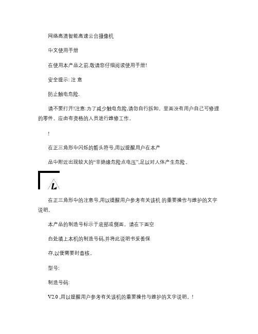
!在正三角形中闪烁的箭头符号,用以提醒用户在本产品中附近出现较大的“非绝缘危险点电压”,足以对人体产生危险。
在正三角形中的注意号,用以提醒用户参考有关该机的重要操作与维护的文字说明。
本产品的制造号标示于底部或侧面。
请在下面空白处填上本机的制造号码,并将此说明书妥善保存,以便需要时查核。
型号:制造号码:V2.0 ,用以提醒用户参考有关该机的重要操作与维护的文字说明。
!目录注意事项 (1第一章功能特点 (3 1.1 云台规格 (31.2 云台基本参数 (3 1.3 云台报警 (31.4 网络参数 (41.5 云台功能 (6第二章网络设臵 (7 2.1 系统连接图 (7 2.2 登录网络 (82.3 预览视频 (10 2.4 设备参数 (15 2.5 语音对讲 (29 2.6 文件管理 (29 2.7 远程回放 (32 2.8 本地设臵 (362.9 设备录像 (373.0 注销重启 (37第三章云台设定 (383.1 系统连接 (383.2 云台拨码设定 (383.3 协议和默认波特率选设定 (403.4 通信波特率的设定 (41第四章安装说明 (434.1 安全措施 (434.2 警告 (434.3 环境要求 (444.4 布线安全 (444.5 安装准备 (444.6 安装方式简介 (464.7 安装说明 (464.8 云台的出线说明 (50附录Ⅰ:系统参数表 (52附录Ⅱ:常见故障分析 (58附录Ⅲ:24VAC 线径和传输距离关系表 (59 附录Ⅳ:防雷击、浪涌 (61附录Ⅴ:维修服务条款 (62注意事项:电气安全在本产品安装使用中必须严格遵守国家和地区各项电气标准。
配用本机自带的专用电源。
TPS70445PWP中文资料

description
The TPS704xx family of devices consists of dual-output low-dropout voltage regulators with integrated SVS (RESET, POR, or power on reset) and power good (PG) functions. These devices are capable of supplying 1 A and 2 A by regulator 1 and regulator 2 respectively. Quiescent current is typically 185 µA at full load. Differentiated features, such as accuracy, fast transient response, SVS supervisory circuit (power on reset), manual reset input, and independent enable functions provide a complete system solution.
PRODUCTION DATA information is current as of publication date. Products conform to specifications per the terms of Texas Instruments standard warranty. Production processing does not necessarily include testing of all parameters.
元器件交易网
抗生素中英文对照表
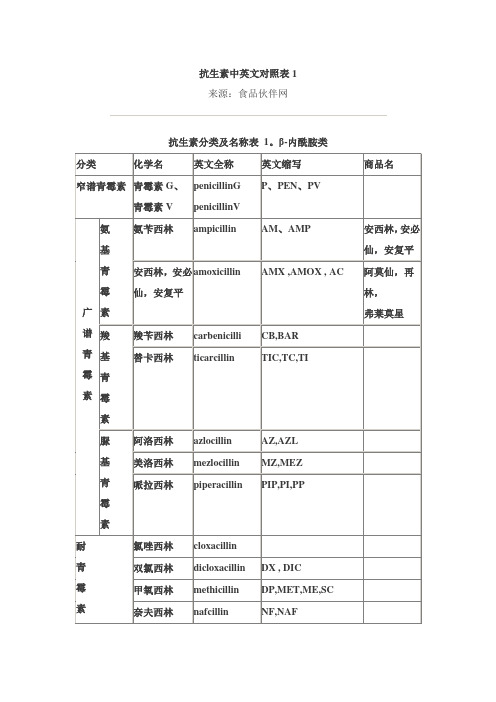
抗生素中英文对照表1来源:食品伙伴网抗生素分类及名称表1。
β-内酰胺类抗生素分类及名称表 2. 非β-内酰胺类AE自带特效中英文对照表3D Channel三维通道特效--3d chanel extract 提取三维通道--depth matte深度蒙版--depth of field场深度--fog 3D雾化--ID Matte ID蒙版Blur & Sharpen模糊与锐化特效--box blur方块模糊--channel blur通道模糊--compound blur混合模糊--directional blur方向模糊--fast blur快速模糊--gaussuan blur高斯模糊--lens blur镜头虚化模糊--radial blur径向模糊--reduce interlace flicker降低交错闪烁--sharpen锐化--smart blur智能模糊--unshart mask反遮罩锐化Channel通道特效--alpha levels Alpha色阶--arithmetic通道运算--blend混合--calculations融合计算--channel combiner复合计算--invert反相--minimax扩亮扩暗--remove color matting删除蒙版颜色--set channels设置通道--set matte设置蒙版--shift channels转换通道--solid composite实体色融合Color correction 颜色校正--auto color自动色彩调整--auto contrast自动对比度--auto levels自动色阶--brightness & contrast亮度核对比度--broadcast colors播放色--change color转换色彩--change to color颜色替换--channel mixer通道混合--color balance色彩平衡--color blance(HIS)色彩平衡(HIS)--color link色彩连接--color stabilizer色彩平衡器--colorama彩光--curves曲线调整--equalize均衡效果--exposure多次曝光--gamma/pedestal/gain伽马/基色/增益--hue/saturation色相/饱和度--leave color退色--levels (individual controls)色阶(个体控制) --photo filter照片过滤--PS arbitrary Map映像遮罩--shadow/highlight阴影/高光--tint 浅色调/色度--tritone三阶色调整Distort扭曲特效--bezier warp贝赛尔曲线弯曲--bulge凹凸镜--corner pin边角定位--displacement map置换这招--liquify像素溶解变换--magnify像素无损放大--mesh warp液态变形--mirror镜像--offset位移--optics compensation镜头变形--polar coordinates极坐标转换--puppet木偶工具--reshape形容--ripple波纹--smear涂抹--spherize球面化--transform变换--turbulent displace变形置换--twirl扭转--warp歪曲边框--wave warp波浪变形Expression Controls表达式控制特效--angel control角度控制--checkbox control检验盒控制--color control色彩控制--layer control层控制--point control点控制--slider control游标控制Generate 生成--4-ccolor gradient四色渐变--advanced lightning高级闪电--audio spectrum声谱--audio waveform声波--beam声波--beam光束--cell pattern单元图案--checkerboard棋盘格式--circle圆环--ellipse椭圆--eyedropper fill滴管填充--fill填充--fractal万花筒--grid网格--lens flare镜头光晕--lightning闪电--paint bucker颜料桶--radio waves电波--ramp渐变--scribble涂抹--stroke描边--vegas勾画--write-on手写效果Keying 抠像特效--color difference key色彩差抠像--difference matte差异蒙版(已淘汰)--extract提取(已淘汰)--inner/outer key轮廓抠像--luma key亮度抠像--color key色彩抠像(效果差)--color range色彩范围(效果较差)--linear color key线性色彩抠像(与spill suppressor配合使用,效果可以接受)--spill suppressor溢色控制常用的抠图滤镜keylight(1.2),通过调节Screen color,Screen Gain, Screen Balance三个参数调节,简单方便效果不错Matte 蒙版特效--matte choker蒙版清除--simple choker简单清除--Noise & Grain 噪波和杂点特效--add grain添加杂点--dust & scratches杂点和划痕--fractal noise不规则噪波--match grain杂点匹配--median中性--noise杂点--noise alpha alpha通道杂点--noise HLS HLS通道杂点--noise HLS auto自动生成HLS通道杂点--remove grain减弱杂点Paint 绘画--paint绘画工具--vector paint矢量绘画perspective 透视--3D glasses立体眼镜--basic 3D基础三维--bevel Alpha 斜面Alpha--vevel edges边缘导角--drop shadow阴影--radial shadow放射状的投影simulation 仿真特效--CC Ball Action CC 滚珠操作--CC Bubbles CC 吹泡泡--CC Drizzle CC 细雨滴--CC Hair CC 毛发--CC Mr.Mercury CC 水银滴落--CC Particle Systems Ⅱ CC 粒子仿真系统--CC Particle World CC 粒子仿真世界--CC Pixel Polly CC 像素多边形--CC Rain CC 下雨--CC Scatterize CC 散射效果--CC Snow CC 下雪--CC Star Burst CC 星爆--card dance碎片飘移--caustics焦散--foam泡沫--particle playground粒子--shatter爆碎--wave world波纹抖动stylize 风格化特效--brush storkes画笔描边--color emboss彩色浮雕--emboss浮雕--find edges查找边缘--glow辉光--mosaic马赛克--motion tile运动拼贴--posterize多色调分离--roughen edges粗糙边缘--scatter扩散--strobe light闪光灯--texturize纹理化--threshold对比度极限text 文字特效--basic text基本文字--numbers数字--path text路径文字--timecode时间码time 时间特效--echo重影--psterize time招贴画--time difference时间差异--time displacement时间置换--timewarp时间收缩transition 转场特效--block dissolve快面溶解--card wipe卡片擦除--gradient wipe渐变擦拭--iris wipe星形擦拭--linear wipe线性擦拭--radial wipe径向擦拭--venetian blinds百叶窗utlity 实用特效--cineon converter Cineon转换--color profile converter色彩特性描述转换--grow bounds范围增长--HDR compander HDR压缩扩展--HDR Highlight compression HDR高光压缩Audio音频特效--backwards倒播--bass & treble低音和高音--delay延迟--flange & chorus变调和合声--high-low pass高低音过滤--modulator调节器--parametric EQ EQ参数--reverb回声--stero mixer 立体声混合--tone音质AE的FOAM特效介绍在AfterEffect中有一组滤镜叫做Simulation,这是一组仿真滤镜,利用它可以来模拟自然界中的泡沫、光的反射、爆炸、水纹等效果,下面我们通过实例来介绍一下其中的Foam特效的使用。
PT7V3727W中文资料

Product Features• 3.3v/5.0v operating voltage• Uses an inexpensive external crystal• On-chip VCXO with pull range of 240ppm • VCXO tuning voltage from 0 to 3.3V • 10mA output driver at CMOS levels • Available in SOIC packageOrdering InformationOrdering code Package type Operating Range PT7V2727W 8-Pin SOIC Industrial PT7V3727W 8-Pin SOIC IndustrialLogic Block DiagramPin ConfigurationPin DescriptionPin Number2727 3727 Pin Name Type Description1, 8 1, 8 X1, X2 I Crystal Connection, Connect to a pullable 27MHz crystal 2, 7 6 NC No Connect, Can be float or connected to V CC or GND 3 3 V IN I Voltage Input to VCXO 4 4, 7 GND PWR Ground 5 5 CLKOUT O Clock Output 6 2 V CC PWR Power Supply +3.3v/5.0vGeneral DescriptionThe PT7V2727/3727 are low-cost, high-performance 3.3V /5.0v VCXO, designed to replace expensive VCXO modules. The on-chip voltage causes clocks to vary by ±120ppm.They use an inexpensive external pullable crystal at 27MHz to produce the same output frequency.Applicationsz Set-Top Box zxDSL12345678X1VINGNDNC X2NC Vcc PT7V2727SOIC 8 packageCLKOUT12345678X1VIN GNDVcc X2GND NC CLKOUTPT7V3727SOIC 8 packageMaximum Ratings(Above which the useful life may be impaired. For userguidelines, not tested.)DC Electrical Characteristics(Unless otherwise specified, V CC = 3.3V, f O = 27MHz, V IN = 1.65V, Load = 15pF, T A = 25o C)Sym. Parameter TestConditionPinMin.Typ.Max.UnitV CC SupplyVoltage V CC 3.153 3.3 3.465VI CC SupplyCurrent OE = 3.3V,C L = 15pFV CC 5 mAI OH High-level output voltage V OH = V CC-0.5V CLKOUT -11 -4I OL Low-level output voltage V OL = 0.5V CLKOUT 4 12mAR S *Negative Resistance V IN = 0V X1, X2 -150 Ωf Input Frequency X1, X2 20 27 30 MHzC L Output Capacitance CLKOUT 15 30 pF* Note: only reference for design.AC Electrical Characteristics(Unless otherwise specified, f O = 27MHz, Load = 15pF, T A = 25o C)Sym. Parameter TestConditionPinMin.Typ.Max.Unitt r / t f Rise / Fall time 0.1V CC to 0.9V CC CLKOUT 1.5 6 nsDuty Output clock duty cycle At V CC/2 CLKOUT455055% ∆f Output frequency pull range V IN from 0V to V CC±120 ppmt j Cycle to cycle jitter 50 ps Linearity V IN from 0.1 to 0.9V CC±10 %Oscillator start time Trigger at 0.9V CC 1.5 10 msRecommended Crystal SpecificationsDescription CrystalMode of Oscillation FundamentalFrequency Range 27.000MHzFrequency Tolerance ±30ppmTemperature plus Aging Stability ±50ppmOperating Temperature -20ºC to + 70ºCC0/C1 240(max.) Load Capacitance(C L) 18pFEquivalent Series Resistance(ESR) 35ohms(max.)Plastic 8-pin SOIC (W) PackageNotesPericom Technology Inc.Email: support@ Web Site: , China: No. 20 Building, 3/F, 481 Guiping Road, Shanghai, 200233, ChinaTel: (86)-21-6485 0576 Fax: (86)-21-6485 2181Asia Pacific: Unit 1517, 15/F, Chevalier Commercial Centre, 8 Wang Hoi Rd, Kowloon Bay, Hongkong Tel: (852)-2243 3660 Fax: (852)- 2243 3667U.S.A.: 3545 North First Street, San Jose, California 95134, USATel: (1)-408-435 0800 Fax: (1)-408-435 1100Pericom Technology Incorporation reserves the right to make changes to its products or specifications at any time, without notice, in order to improve design or performance and to supply the best possible product. Pericom Technology does not assume any responsibility for use of any circuitry described other than the circuitry embodied in Pericom Technology product. The company makes no representations that circuitry described herein is free from patent infringement or other rights, of Pericom Technology Incorporation.。
CDRH64BNP-47OMB中文资料

1.外形1-1.寸法図(mm)* 公差のない寸法は参考値とする。
1-2.捺印表示例 O-3.推奨ランド図(mm)2.コイル仕様2-1.端子接続図(裏面図)電極(端子)間の隙間はシルク処理をして御使用下さい。
捺印位置不定製造密番頭部直捺印100電極側電極側compliance Cd:Max.0.01wt%others:Max.0.1wt%RoHS12-2.電気的特性Ⅰ(リール梱包の場合)NO. 品 名 表示 インダクタンス[以内]※1D.C.R.(Ω)[以下](at 20℃)※2定格電流(A)※3スミダコード0102 CDRH64BNP-1ØØMCCDRH64BNP-12ØMC10012010μH ± 20%12μH ± 20%0.12 (88m)0.13 (97m)1.351.204745-01454745-01460304 CDRH64BNP-15ØMCCDRH64BNP-18ØMC15018015μH ± 20%18μH ± 20%0.18 (0.13)0.24 (0.18)1.101.004745-01474745-01480506 CDRH64BNP-22ØMCCDRH64BNP-27ØMC22027022μH ± 20%27μH ± 20%0.27 (0.20)0.30 (0.22)0.910.824745-01494745-01500708 CDRH64BNP-33ØMCCDRH64BNP-39ØMC33039033μH ± 20%39μH ± 20%0.33 (0.25)0.37 (0.27)0.750.694745-01514745-01520910 CDRH64BNP-47ØMCCDRH64BNP-56ØMC47056047μH ± 20%56μH ± 20%0.52 (0.38)0.56 (0.41)0.620.584745-01544745-01551112 CDRH64BNP-68ØMCCDRH64BNP-82ØMC68082068μH ± 20%82μH ± 20%0.63 (0.47)0.71 (0.53)0.520.474745-01564745-01571314 CDRH64BNP-1Ø1MCCDRH64BNP-121MC101121100μH ± 20%120μH ± 20%1.03 (0.76)1.15 (0.85)0.430.394745-01584745-01591516 CDRH64BNP-151MCCDRH64BNP-181MC151181150μH ± 20%180μH ± 20%1.68 (1.29)1.87 (1.44)0.350.324745-01604745-01611718 CDRH64BNP-221MCCDRH64BNP-271MC221271220μH ± 20%270μH ± 20%2.08 (1.60)2.37 (1.82)0.290.264745-01624745-01631920 CDRH64BNP-331MCCDRH64BNP-391MC331391330μH ± 20%390μH ± 20%2.67 (2.05)2.94 (2.26)0.230.224745-01654745-01662122 CDRH64BNP-471MCCDRH64BNP-561MC471561470μH ± 20%560μH ± 20%3.93 (3.02)5.43 (4.18)0.200.184745-01674745-01682324 CDRH64BNP-681MCCDRH64BNP-821MC681821680μH ± 20%820μH ± 20%7.32 (5.63)8.24 (6.34)0.170.154745-01694745-017025 CDRH64BNP-1Ø2MC 102 1 mH ± 20% 9.26 (7.13) 0.14 4745-0171※1: 測定周波数 L at 1 kHz※2: ( )内は、標準値とする。
ZB4BS964中文资料(telemecanique)中文数据手册「EasyDatasheet - 矽搜」

芯片中文手册,看全文,戳
产品数据表
特点
互补 CAD总宽度 CAD整体高度 CAD整体深度
产品重量 耐高压清洗机 机械寿命 电气组成代码
环境
防护护处理 环境空气温度储存 环境空气温度运行 防触电防护护等级
防护护IP等级 防护NEMA等级 防护IK等级
标准
产品认证
ZB4BS964
红Ø60急停按钮EC 61140
IP66符合IEC 60529
NEMA 13 NEMA 4 NEMA 4X NEMA 12
IK03符合IEC 50102
EN/IEC 60204-1 EN/IEC 60947-1 EN/IEC 60947-5-1 EN/IEC 60947-5-4 EN/IEC 60947-5-5 EN/ISO 13850 JIS C 4520 UL 508 GB 14048.5 CSA C22.2第14号
中央
60 mm
60 mm
79 mm
0.118千克
7000000帕在55℃,距离:0.1米
300000周期
C11为= 3 触点使用前安装单块 C15 1 触点使用前安装单块 C7为= 4 触点使用前安装单块 C8为= 4 触点使用前安装单,双块 C10为= 4 触点使用前安装单,双块
TH
-40...70 °C
A: 1.18英寸分钟. B: 1.57英寸分钟.
面板和印刷电路电路板一般公差
累产品公差不得超过0.3毫米/ 0.012中:T1 + T2 = 0.3 mm最大.
安装注意事项
电路线路板最小厚度:2.6毫米/0.06英寸
切出直径:22.4毫米±0.1 / 0.88±0.004. 身体/固定套环ZB4 BZ009方向:±2
75176B中文资料

PACKAGING INFORMATIONOrderable Device Status(1)PackageType PackageDrawingPins PackageQtyEco Plan(2)Lead/Ball Finish MSL Peak Temp(3)SN65176BD ACTIVE SOIC D875Green(RoHS&no Sb/Br)CU NIPDAU Level-1-260C-UNLIMSN65176BDE4ACTIVE SOIC D875Green(RoHS&no Sb/Br)CU NIPDAU Level-1-260C-UNLIMSN65176BDG4ACTIVE SOIC D875Green(RoHS&no Sb/Br)CU NIPDAU Level-1-260C-UNLIMSN65176BDR ACTIVE SOIC D82500Green(RoHS&no Sb/Br)CU NIPDAU Level-1-260C-UNLIMSN65176BDRE4ACTIVE SOIC D82500Green(RoHS&no Sb/Br)CU NIPDAU Level-1-260C-UNLIMSN65176BDRG4ACTIVE SOIC D82500Green(RoHS&no Sb/Br)CU NIPDAU Level-1-260C-UNLIMSN65176BP ACTIVE PDIP P850Pb-Free(RoHS)CU NIPDAU N/A for Pkg TypeSN65176BPE4ACTIVE PDIP P850Pb-Free(RoHS)CU NIPDAU N/A for Pkg TypeSN75176BD ACTIVE SOIC D875Green(RoHS&no Sb/Br)CU NIPDAU Level-1-260C-UNLIMSN75176BDE4ACTIVE SOIC D875Green(RoHS&no Sb/Br)CU NIPDAU Level-1-260C-UNLIMSN75176BDG4ACTIVE SOIC D875Green(RoHS&no Sb/Br)CU NIPDAU Level-1-260C-UNLIMSN75176BDR ACTIVE SOIC D82500Green(RoHS&no Sb/Br)CU NIPDAU Level-1-260C-UNLIMSN75176BDRE4ACTIVE SOIC D82500Green(RoHS&no Sb/Br)CU NIPDAU Level-1-260C-UNLIMSN75176BDRG4ACTIVE SOIC D82500Green(RoHS&no Sb/Br)CU NIPDAU Level-1-260C-UNLIMSN75176BP ACTIVE PDIP P850Pb-Free(RoHS)CU NIPDAU N/A for Pkg TypeSN75176BPE4ACTIVE PDIP P850Pb-Free(RoHS)CU NIPDAU N/A for Pkg TypeSN75176BPSR ACTIVE SO PS82000Green(RoHS&no Sb/Br)CU NIPDAU Level-1-260C-UNLIMSN75176BPSRG4ACTIVE SO PS82000Green(RoHS&no Sb/Br)CU NIPDAU Level-1-260C-UNLIM(1)The marketing status values are defined as follows:ACTIVE:Product device recommended for new designs.LIFEBUY:TI has announced that the device will be discontinued,and a lifetime-buy period is in effect.NRND:Not recommended for new designs.Device is in production to support existing customers,but TI does not recommend using this part in a new design.PREVIEW:Device has been announced but is not in production.Samples may or may not be available.OBSOLETE:TI has discontinued the production of the device.(2)Eco Plan-The planned eco-friendly classification:Pb-Free(RoHS),Pb-Free(RoHS Exempt),or Green(RoHS&no Sb/Br)-please check /productcontent for the latest availability information and additional product content details.TBD:The Pb-Free/Green conversion plan has not been defined.Pb-Free(RoHS):TI's terms"Lead-Free"or"Pb-Free"mean semiconductor products that are compatible with the current RoHS requirements for all6substances,including the requirement that lead not exceed0.1%by weight in homogeneous materials.Where designed to be soldered at high temperatures,TI Pb-Free products are suitable for use in specified lead-free processes.Pb-Free(RoHS Exempt):This component has a RoHS exemption for either1)lead-based flip-chip solder bumps used between the die andpackage,or2)lead-based die adhesive used between the die and leadframe.The component is otherwise considered Pb-Free(RoHS compatible)as defined above.Green(RoHS&no Sb/Br):TI defines"Green"to mean Pb-Free(RoHS compatible),and free of Bromine(Br)and Antimony(Sb)based flame retardants(Br or Sb do not exceed0.1%by weight in homogeneous material)(3)MSL,Peak Temp.--The Moisture Sensitivity Level rating according to the JEDEC industry standard classifications,and peak solder temperature.Important Information and Disclaimer:The information provided on this page represents TI's knowledge and belief as of the date that it is provided.TI bases its knowledge and belief on information provided by third parties,and makes no representation or warranty as to the accuracy of such information.Efforts are underway to better integrate information from third parties.TI has taken and continues to take reasonable steps to provide representative and accurate information but may not have conducted destructive testing or chemical analysis on incoming materials and chemicals.TI and TI suppliers consider certain information to be proprietary,and thus CAS numbers and other limited information may not be available for release.In no event shall TI's liability arising out of such information exceed the total purchase price of the TI part(s)at issue in this document sold by TI to Customer on an annual basis.TAPE AND REEL INFORMATIONDevice Package Pins Site ReelDiameter(mm)ReelWidth(mm)A0(mm)B0(mm)K0(mm)P1(mm)W(mm)Pin1QuadrantSN65176BDR D8FMX33012 6.4 5.2 2.1812Q1 SN75176BDR D8FMX33012 6.4 5.2 2.1812Q1 SN75176BPSR PS8MLA330168.2 6.6 2.51216Q1TAPE AND REEL BOX INFORMATIONDevice Package Pins Site Length(mm)Width(mm)Height(mm)SN65176BDR D8FMX338.1340.520.64SN75176BDR D8FMX338.1340.520.64SN75176BPSR PS8MLA342.9336.628.58IMPORTANT NOTICETexas Instruments Incorporated and its subsidiaries (TI)reserve the right to make corrections,modifications,enhancements,improvements,and other changes to its products and services at any time and to discontinue any product or service without notice.Customers should obtain the latest relevant information before placing orders and should verify that such information is current and complete.All products are sold subject to TI’s terms and conditions of sale supplied at the time of order acknowledgment.TI warrants performance of its hardware products to the specifications applicable at the time of sale in accordance with TI’s standard warranty.Testing and other quality control techniques are used to the extent TI deems necessary to support this warranty.Except where mandated by government requirements,testing of all parameters of each product is not necessarily performed.TI assumes no liability for applications assistance or customer product design.Customers are responsible for their products and applications using TI components.To minimize the risks associated with customer products and applications,customers should provide adequate design and operating safeguards.TI does not warrant or represent that any license,either express or implied,is granted under any TI patent right,copyright,mask work right,or other TI intellectual property right relating to any combination,machine,or process in which TI products or services are rmation published by TI regarding third-party products or services does not constitute a license from TI to use such products or services or a warranty or endorsement e of such information may require a license from a third party under the patents or other intellectual property of the third party,or a license from TI under the patents or other intellectual property of TI.Reproduction of information in TI data books or data sheets is permissible only if reproduction is without alteration and isaccompanied by all associated warranties,conditions,limitations,and notices.Reproduction of this information with alteration is an unfair and deceptive business practice.TI is not responsible or liable for such altered documentation.Resale of TI products or services with statements different from or beyond the parameters stated by TI for that product or service voids all express and any implied warranties for the associated TI product or service and is an unfair and deceptive business practice.TI is not responsible or liable for any such statements.TI products are not authorized for use in safety-critical applications (such as life support)where a failure of the TI product would reasonably be expected to cause severe personal injury or death,unless officers of the parties have executed an agreementspecifically governing such use.Buyers represent that they have all necessary expertise in the safety and regulatory ramifications of their applications,and acknowledge and agree that they are solely responsible for all legal,regulatory and safety-related requirements concerning their products and any use of TI products in such safety-critical applications,notwithstanding any applications-related information or support that may be provided by TI.Further,Buyers must fully indemnify TI and itsrepresentatives against any damages arising out of the use of TI products in such safety-critical applications.TI products are neither designed nor intended for use in military/aerospace applications or environments unless the TI products are specifically designated by TI as military-grade or "enhanced plastic."Only products designated by TI as military-grade meet military specifications.Buyers acknowledge and agree that any such use of TI products which TI has not designated as military-grade is solely at the Buyer's risk,and that they are solely responsible for compliance with all legal and regulatory requirements in connection with such use.TI products are neither designed nor intended for use in automotive applications or environments unless the specific TI products are designated by TI as compliant with ISO/TS 16949requirements.Buyers acknowledge and agree that,if they use any non-designated products in automotive applications,TI will not be responsible for any failure to meet such requirements.Following are URLs where you can obtain information on other Texas Instruments products and application solutions:ProductsApplications AmplifiersAudioDataConvertersAutomotiveDSPBroadband InterfaceDigital Control LogicMilitary Power MgmtOptical Networking MicrocontrollersSecurity RFIDTelephony Low PowerVideo &ImagingWireless Wireless Mailing Address:Texas Instruments,Post Office Box 655303,Dallas,Texas 75265Copyright ©2007,Texas Instruments Incorporated 元器件交易网。
BUZ77B中文资料

SIPMOS ®Power Transistor• N channel• Enhancement mode • Avalanche-ratedPin 1Pin 2Pin 3GDSType V DS I D R DS(on )Package Ordering Code BUZ 77 B600 V2.9 A3.5 ΩTO-220 ABC67078-S1320-A5Maximum Ratings ParameterSymbolValues Unit Continuous drain currentT C = 29 °CI D 2.9APulsed drain currentT C = 25 °CI Dpuls11.5Avalanche current,limited by T jmaxI AR 2.7Avalanche energy,periodic limited by T jmax E AR 5mJAvalanche energy, single pulseI D = 2.7 A, V DD = 50 V, R GS = 25 ΩL = 45.3 mH, T j = 25 °C E AS180Gate source voltage V GS ± 20V Power dissipationT C = 25 °CP tot75WOperating temperature T j -55 ... + 150°C Storage temperatureT stg -55 ... + 150Thermal resistance, chip case R thJC ≤ 1.67K/WThermal resistance, chip to ambient R thJA75DIN humidity category, DIN 40 040 E IEC climatic category, DIN IEC 68-155 / 150 / 56Electrical Characteristics, at T j = 25°C, unless otherwise specifiedParameter Symbol Values Unitmin.typ.max.Static CharacteristicsDrain- source breakdown voltage V GS = 0 V, I D = 0.25 mA, T j = 25 °C V(BR)DSS600--VGate threshold voltage V GS=V DS, I D = 1 mA V GS(th)2.1 3 4Zero gate voltage drain currentV DS = 600 V, V GS = 0 V, T j = 25 °C V DS = 600 V, V GS = 0 V, T j = 125 °C I DSS--100.11001µAGate-source leakage current V GS = 20 V, V DS = 0 V I GSS- 10 100nADrain-Source on-resistance V GS = 10 V, I D = 1.7 A R DS(on)- 3 3.5ΩElectrical Characteristics, at T j = 25°C, unless otherwise specifiedParameter Symbol Values Unitmin.typ.max. Dynamic CharacteristicsTransconductanceV DS≥ 2 *I D * R DS(on)max, I D = 1.7 A g fs1.53-SInput capacitanceV GS = 0 V, V DS = 25 V, f = 1 MHz C iss- 460 690pFOutput capacitanceV GS = 0 V, V DS = 25 V, f = 1 MHz C oss- 55 85Reverse transfer capacitanceV GS = 0 V, V DS = 25 V, f = 1 MHz C rss- 20 30Turn-on delay timeV DD = 30 V, V GS = 10 V, I D = 2 A R GS = 50 Ωt d(on)-812nsRise timeV DD = 30 V, V GS = 10 V, I D = 2 A R GS = 50 Ωt r- 30 40Turn-off delay timeV DD = 30 V, V GS = 10 V, I D = 2 A R GS = 50 Ωt d(off)- 50 65Fall timeV DD = 30 V, V GS = 10 V, I D = 2 A R GS = 50 Ωt f- 30 40Electrical Characteristics, at T j = 25°C, unless otherwise specifiedParameter Symbol Values Unitmin.typ.max. Reverse DiodeInverse diode continuous forward current T C = 25 °C I S-- 2.7AInverse diode direct current,pulsed T C = 25 °C I SM-- 11Inverse diode forward voltage V GS = 0 V, I F = 5.4 A V SD- 0.95 1.3VReverse recovery timeV R = 100 V, I F=l S, d i F/d t = 100 A/µs t rr- 350-nsReverse recovery chargeV R = 100 V, I F=l S, d i F/d t = 100 A/µs Q rr- 3.5-µCDrain current I D = ƒ(T C )parameter: V GS ≥ 10 V20406080100120°C 160T C0.0 0.2 0.4 0.60.8 1.0 1.2 1.4 1.61.82.02.2 2.4 2.6A3.0 IDPower dissipation P tot = ƒ(T C )20406080100120°C 160T C0 10 2030405060W 80P totSafe operating area I D = ƒ(V DS )parameter: D = 0.01, T C = 25°C10 10 10 10 I DV DS Transient thermal impedance Z th JC = ƒ(t p )parameter: D = t p / T10 10 10 10 10 Z thJC10101010101010 10s t pTyp. output characteristics I D = ƒ(V DS )parameter: t p = 80 µs10203040V60V DSI DlTyp. drain-source on-resistance R DS (on) = ƒ(I D )parameter: V GS0.01.02.03.04.0A 6.0I DR DS (on)Typ. transfer characteristics I D = f (V GS )parameter: t p = 80 µs V DS ≥2 x I D x R DS(on)max12345678V10V GS 0.0 0.2 0.4 0.6 0.8 1.01.21.4 1.6 1.8 A2.2 I DTyp. forward transconductance g fs = f (I D )parameter: t p = 80 µs,V DS ≥2 x I D x R DS(on)max0.00.20.40.60.8 1.0 1.2 1.4 1.6 1.8A 2.2I D0.00.40.8 1.2 1.62.02.4 2.83.2 S4.0 g fsGate threshold voltageV GS (th) = ƒ(T j)parameter: V GS = V DS, I D = 1 mAVGS(th)-60-202060100°C160Tj Drain-source on-resistanceR DS (on) = ƒ(T j)parameter: I D = 1.7 A, V GS = 10 V-60-202060100°C160TjRDS (on)Typ. capacitancesC = f (V DS)parameter:V GS = 0V, f = 1MHz051015202530V40VDS10101010CForward characteristics of reverse diodeI F = ƒ(V SD)parameter: T j, t p = 80 µs10101010IF0.00.40.8 1.2 1.6 2.0 2.4V 3.0VSDAvalanche energy E AS = ƒ(T j )parameter: I D = 2.7 A, V DD = 50 V R GS = 25 Ω, L = 45.3 mH20406080100120°C 160T j0 20 40 6080100 120 140 160mJ 190 EASTyp. gate charge V GS = ƒ(Q Gate )parameter: I D puls = 4 A481216202428nC 34Q GateV GSDrain-source breakdown voltage V (BR)DSS = ƒ(T j )-60-202060100°C 160T j540 560 580 600 620 640 660 680V710 V (BR)DSS。
- 1、下载文档前请自行甄别文档内容的完整性,平台不提供额外的编辑、内容补充、找答案等附加服务。
- 2、"仅部分预览"的文档,不可在线预览部分如存在完整性等问题,可反馈申请退款(可完整预览的文档不适用该条件!)。
- 3、如文档侵犯您的权益,请联系客服反馈,我们会尽快为您处理(人工客服工作时间:9:00-18:30)。
Rev.B
2/4
元器件交易网
PTZ7.5B
Diodes
Electrical characteristic curves (Ta=25°C)
100 5.1 4.7 4.3 10 3.9 3.6 5.6 6.2 6.8 7.5 8.2 9.1 10 11 12 13 15 16 18 20 22 24 27 30 33 36
Operating resistance : Zz(Ω) Reverse current : IR(μA)
Temperature coefficiency : *γz(mV/℃) ESD Break down voltage : ESD(kV)
Iz(mA) Max. Iz(mA) MAX. VR(V) Iz(mA) MIN. TYP. PTZ 3.6B 40 15 40 60 40 1.0 -2.8 PTZ 3.9B 40 15 40 40 40 1.0 -2.4 PTZ 4.3B 4.300 40 40 40 4.572 4.800 15 20 1.0 -2.1 PTZ 4.7B 4.700 40 40 40 4.924 5.200 10 20 1.0 -1.7 PTZ 5.1B 5.100 40 40 40 5.368 5.700 8 20 1.5 -0.6 PTZ 5.6B 5.600 40 40 40 5.856 6.300 8 20 2.5 1.4 PTZ 6.2B 6.200 40 40 40 6.509 7.000 6 20 3.0 2.5 PTZ 6.8B 6.800 40 40 40 7.280 7.700 6 20 3.5 3.2 PTZ 7.5B 7.500 40 40 40 7.889 8.400 4 20 4.0 4.2 PTZ 8.2B 8.200 40 40 40 8.655 9.300 4 20 5.0 5.0 PTZ 9.1B 9.100 40 40 40 9.747 10.200 6 20 6.0 5.9 PTZ 10B 10.000 40 40 40 10.310 11.200 6 10 7.0 6.9 30kV PTZ 11B 11.000 20 20 20 11.510 12.300 8 10 8.0 7.9 PTZ 12B 12.000 20 20 20 12.500 13.500 8 10 9.0 8.7 PTZ 13B 13.300 20 20 20 13.820 15.000 10 10 10.0 10.1 PTZ 15B 14.700 20 20 20 15.350 16.500 10 10 11.0 11.8 PTZ 16B 16.200 20 20 20 16.860 18.300 12 10 12.0 13.3 PTZ 18B 18.000 20 20 20 19.000 20.300 12 10 13.0 15.0 PTZ 20B 20.000 20.820 20 14 20 15.0 17.4 20 22.400 10 PTZ 22B 22.000 23.850 10 14 10 17.0 19.4 10 24.500 10 PTZ 24B 24.000 10 16 10 25.310 27.600 10 10 19.0 21.6 PTZ 27B 27.000 10 16 10 28.700 30.800 10 10 21.0 24.6 PTZ 30B 30.000 10 18 10 31.570 34.000 10 10 23.0 27.5 PTZ 33B 33.000 10 18 10 34.950 37.000 10 10 25.0 30.8 PTZ 36B 36.000 39.240 40.000 10 20 10 10 27.0 37.0 10 1.The Zener voltage(Vz) is measured 40ms after power is supplied. 2.The operating resistances(Zz、Zzk) are measured by superimposing a minute alternating current on the regulated current(Iz). TYP. 3.813 4.136
8.1 ZENER VOLTAGE:Vz(V)
8
7.9 AVE:7.889V 7.8
7.7 Vz DISPERSION MAP
0
IR DISPERSION MAP
Ct DISPERSION MAP
100 ELECTROSTATIC DDISCHARGE TEST ESD(KV)
30 25 20 15 10 5 No break at 30kV
DYNAMIC IMPEDANCE:Zz(Ω)
10
1
0.1 0.1 1 ZENER CURRENT:Iz(mA) Zz-Iz CHARACTERISTICS 10
0 C=200pF R=0Ω C=100pF R=1.5kΩ C=150pF R=330Ω
ESD DISPERSION MAP
Rev.B
4/4
10000 PRSM REVERSE SURGE MAXIMUM POWER:PRSM(W) 1000 t
POWER DISSIPATION:Pd(W)
100
10
1 0.001 0.01 0.1 1 10 100
TIME:t(ms) PRSM-TIME CHARACTERISTICS 1000 Mounted on epoxy board
3.6B 3.9B 4.3B 4.7B 5.1B 5.6B 6.2B 6.8B 7.5B
TYP. PTZ 8.2B PTZ 9.1B PTZ 10B PTZ 11B PTZ 12B PTZ 13B PTZ 15B PTZ 16B
TYPE NO.
8.2B 9.1B 10B 11B 12B 13B 15B 16B
MAX. 4.000 4.400
Test Condition
C=150pF R=330Ω forward and reverse : 10 times
Marking (TYPE NO.)
TYP. PTZ 3.6B PTZ 3.9B PTZ 4.3B PTZ 4.7B PTZ 5.1B PTZ 5.6B PTZ 6.2B PTZ 6.8B PTZ 7.5B TYPE NO.
元器件交易网
PTZ7.5B
Diodes
Zener diode
PTZ7.5B
Applications External dimensions (Unit : mm)
2.6±0.2 1.2±0.3
Land size figure (Unit : mm)
2.0
4.5±0.03 2±0.05
IM=10mA IF=0.5A
Rth(j-a) TRANSIENT THAERMAL IMPEDANCE:Rth (℃/W) TEMP.COEFFICIENCE:γz(mV/℃) 100
1ms time
30 25
300us
Rth(j-c) 10
1
0.1 0.001 0.1 10 TIME:t(s) Rth-t CHARACTERISTICS 1000
ZENER CURRENT:Iz(mA)
1
0.1
0.01
0.001 0 5 10 15 20 25 30 35 40 45
ZENER VOLTAGE:Vz(V) Vz-Iz CHARACTERISTICS
1200 1000 800 600 400 200 0 0 25 50 75 100 125 150 AMBIENT TEMPERATURE:Ta(℃) Pd-Ta CHARACTERISTICS 0.12 0.1 0.08 TEMP.COEFFICIENCE:γz(%/℃) 0.06 0.04 20 0.02 0 -0.02 -0.04 -0.06 -0.08 0 20 30 TIME:t(ms) IFSM-t CHARACTERISTICS 10 40 15 10 5 0 -5 40 35
4.0±0.1 2.0±0.05 8.0±0.1 φ1.55±0.1 0 1.75±0.05 0.3±0.1
5.5±0.05
φ1.55±0.05 2.9±0.1 8.0±0.1 2.4±0.1
Absolute maximum ratings (Ta=25°C)
Param eter P ower dis s ipation J unction tem perature S torage tem perature Sym bol P Tj Ts tg Lim its 1000 150 -55 to +150 Unit mW ℃ ℃
1000
0.01
0.001
8.2 Ta=25℃ IZ=40mA n=30pcs
1 0.9 REVERSE CURRENT:IR(nA) 0.8 0.7 0.6 0.5 0.4 0.3 0.2 0.1 AVE:0.150nA Ta=25℃ VR=4.0V n=30pcs
30 29 28 CAPACITANCE BETWEEN TERMINALS:Ct(pF) 27 26 25 24 23 22 21 20 AVE:26.29pF Ta=25℃ f=1MHz VR=0V n=10pcs
0.25 0.5
2.0uction Silicon epitaxial planar
① ②
0.25
0.5
1.03
0.2
Structure
Manufacture Date
ROHM : PMDS JEDEC : SOD-106
Taping dimensions (Unit : mm)
元器件交易网
Appendix
Notes
No technical content pages of this document may be reproduced in any form or transmitted by any means without prior permission of ROHM CO.,LTD. The contents described herein are subject to change without notice. The specifications for the product described in this document are for reference only. Upon actual use, therefore, please request that specifications to be separately delivered. Application circuit diagrams and circuit constants contained herein are shown as examples of standard use and operation. Please pay careful attention to the peripheral conditions when designing circuits and deciding upon circuit constants in the set. Any data, including, but not limited to application circuit diagrams information, described herein are intended only as illustrations of such devices and not as the specifications for such devices. ROHM CO.,LTD. disclaims any warranty that any use of such devices shall be free from infringement of any third party's intellectual property rights or other proprietary rights, and further, assumes no liability of whatsoever nature in the event of any such infringement, or arising from or connected with or related to the use of such devices. Upon the sale of any such devices, other than for buyer's right to use such devices itself, resell or otherwise dispose of the same, no express or implied right or license to practice or commercially exploit any intellectual property rights or other proprietary rights owned or controlled by ROHM CO., LTD. is granted to any such buyer. Products listed in this document are no antiradiation design.