SIOV_General from EPCOS
压敏电阻 突波吸收器--S10K14AUTO 规格书 datasheet
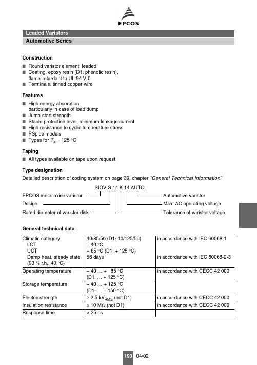
ConstructionI Round varistor element, leadedI Coating: epoxy resin (D1: phenolic resin),flame-retardant to UL 94 V-0I Terminals: tinned copper wire FeaturesI High energy absorption,particularly in case of load dump I Jump-start strengthI Stable protection level, minimum leakage current I High resistance to cyclic temperature stress I PSpice modelsITypes for T A = 125 °CTapingI All types available on tape upon requestType designationDetailed description of coding system on page 39, chapter “General Technical Information ”General technical data Climatic category LCT UCTDamp heat, steady state (93 % r.h., 40 °C)40/85/56 (D1: 40/125/56)– 40 °C+ 85 °C (D1: + 125 °C)56 daysin accordance with IEC 60068-1in accordance with IEC 60068-2-3Operating temperature – 40 … + 85 °C (D1: … + 125 °C)in accordance with CECC 42 000Storage temperature – 40 … + 125 °C (D1: … + 150 °C)Electric strength ³ 2,5 kV RMS (not D1)in accordance with CECC 42 000Insulation resistance ³ 10 M W (not D1)in accordance with CECC 42 000Response time< 25 nsSIOV-S 14 K 14 AUTODesignRated diameter of varistor disk Automotive varistor Max. AC operating voltage Tolerance of varistor voltageEPCOS metal oxide varistor Leaded Varistors Automotive SeriesC for S (1)V RMSV141414141414171717253030If the maximum loads specified for load dump and jump start are fully utilized, subsequentpolarity reversal of the AUTO varistors is inadmissible.If the load remains under the maximum ratings, polarity reversal may be admissible.Contact EPCOS for consultancy on this kind of problem.Load dump or jump start can decrease the varistor voltage in load direction by max. 15 %.1)Measured in load directionv(1 mA)Max. clamping voltage v V 10431043 1043 1043 1043 1043 1053 1053 1053 1077 1093 1093±mm b max mm 9,0 13,0 12,0 17,0 16,0 23,0 13,0 17,04max.Herausgegeben von EPCOS AGUnternehmenskommunikation, Postfach 801709, 81617 München, DEUTSCHLAND( ++49 89 636 09, FAX (089) 636-2 2689EPCOS AG 2002. Vervielfältigung, Veröffentlichung, Verbreitung und Verwertung dieser Broschüre und ihres Inhalts ohne aus-drückliche Genehmigung der EPCOS AG nicht gestattet.Bestellungen unterliegen den vom ZVEI empfohlenen Allgemeinen Lieferbedingungen für Erzeugnisse und Leistungen der Elek-troindustrie, soweit nichts anderes vereinbart wird.Diese Broschüre ersetzt die vorige Ausgabe.Fragen über Technik, Preise und Liefermöglichkeiten richten Sie bitte an den Ihnen nächstgelegenen Vertrieb der EPCOS AG oder an unsere Vertriebsgesellschaften im Ausland. Bauelemente können aufgrund technischer Erfordernisse Gefahrstoffe ent-halten. Auskünfte darüber bitten wir unter Angabe des betreffenden Typs ebenfalls über die zuständige Vertriebsgesellschaft ein-zuholen.Published by EPCOS AGCorporate Communications, P.O. Box 80 17 09, 81617 Munich, GERMANY( ++49 89 636 09, FAX (089) 636-2 2689EPCOS AG 2002. Reproduction, publication and dissemination of this brochure and the information contained therein without EPCOS’ prior express consent is prohibited.Purchase orders are subject to the General Conditions for the Supply of Products and Services of the Electrical and Electronics Industry recommended by the ZVEI (German Electrical and Electronic Manufacturers’ Association), unless otherwise agreed. This brochure replaces the previous edition.For questions on technology, prices and delivery please contact the Sales Offices of EPCOS AG or the international Representa-tives.Due to technical requirements components may contain dangerous substances. For information on the type in question please also contact one of our Sales Offices.。
capl的test module创建方法

capl的test module创建方法使用CAPL的Test Module创建方法在CANoe软件中,CAPL(Communication Access Programming Language)是一种用于开发和执行测试脚本的编程语言。
通过使用CAPL的Test Module,我们可以创建自定义的测试方法来验证和测试汽车电子控制单元(ECU)的功能。
本文将介绍如何使用CAPL的Test Module创建方法,并提供一些注意事项和示例。
一、创建Test Module要创建一个新的Test Module,可以按照以下步骤进行操作:1. 打开CANoe软件,并选择要创建T est Module的配置文件。
2. 在配置文件资源树中,右键单击“T est Modules”文件夹,并选择“New Test Module”选项。
3. 在弹出的对话框中,输入Test Module的名称和描述,并点击“OK”按钮。
二、添加测试方法在创建Test Module后,可以开始添加测试方法。
每个测试方法都是一个独立的函数,用于执行特定的测试任务。
以下是添加测试方法的步骤:1. 在Test Module资源树中,右键单击创建的Test Module,并选择“New Test Function”选项。
2. 在弹出的对话框中,输入测试方法的名称和描述,并点击“OK”按钮。
3. 在弹出的编辑器中,编写测试方法的代码。
可以使用CAPL语言提供的各种函数和语句来实现所需的功能。
三、编写测试方法代码在编写测试方法代码时,需要遵循CAPL语言的语法规则和最佳实践。
以下是一些编写测试方法代码的注意事项:1. 使用有意义的变量和函数命名,以提高代码的可读性。
2. 使用适当的注释来解释代码的功能和目的。
3. 使用合适的数据类型和数据结构来存储和处理测试数据。
4. 使用条件语句(如if-else语句)和循环语句(如for循环)来控制测试流程和执行逻辑。
saml断言格式 -回复

saml断言格式-回复什么是SAML断言格式?SAML(Security Assertion Markup Language)断言格式是一种用于传输安全身份验证和授权信息的开放标准。
它是一种XML(eXtensible Markup Language)语言,用于在不同的安全域之间传递身份验证和授权信息。
SAML断言格式定义了在身份提供者(IdP)和服务提供者(SP)之间传输的安全断言的结构和内容。
SAML断言格式的核心组成部分是断言(Assertion),它是一个包含有关用户身份认证和授权信息的XML文件。
断言中包含有关用户身份认证和授权的声明。
这些声明经过数字签名,以确保数据的完整性和真实性。
断言中还包含时间戳和其他元数据,以确保断言的有效期和使用条件。
SAML断言格式支持以下三种类型的断言:1. 身份断言(Authentication Assertion):身份断言用于证明用户身份已经经过身份提供者(IdP)验证,并且用户已经经过身份验证。
这种断言是基于用户身份验证凭据(如用户名和密码)的。
2. 授权断言(Attribute Assertion):授权断言包含有关用户被授权访问的资源和执行的操作的信息。
它描述了用户所拥有的权限,以及用户是否已经通过适当的权限检查。
这些断言通常用于在用户登录到服务提供者(SP)之后,向SP提供必要的用户属性。
3. 附加断言(Authorization Decision Assertion):附加断言用于在用户访问受保护资源之前,提供有关用户是否有权访问该资源的决策信息。
这种断言通常是基于预定义的访问策略和权限规则。
SAML断言格式的优点是它提供了一种跨域传输身份验证和授权信息的标准化方式,减少了重复开发和集成不同系统之间的困难。
它还提供了灵活性和可扩展性,可以根据实际需求定制和扩展断言的结构和内容。
此外,SAML断言格式还提供了大量的安全性控制和防止身份欺骗的保护机制。
EPCOS压敏电阻SIOV

压敏电阻选型
压敏电阻能承受更大的浪涌电流,而且其体积越大所能承 受的浪涌电流越大,最大可达几十kA到上百kA;但压敏电阻 的漏电流较大,非线性特性较差(动态电阻较大),大电流时限制 电压较高,且所能耐受的冲击电流的大小随冲击次数的增加而 减小(降额特性),较易老化。TVS管的非线性特性和稳压管 完全一样,动态电阻较小,限制电压较低,且不易老化,使用 寿命长,但通流能力较小(10/1000μs波峰值电流在几A至几 百A之间)。再有就是反应速度不同,TVS管的反应速度极快 为ps级,而压敏电阻反应速度稍慢 为ns级。
主编人:邓晓明 393414380@
PowerPoint Design Template
add your subheading
爱普科斯
SIOV metal oxide varistors
资料由深圳市宇特科技提供制作
术语
压敏电阻: 受电压影响的电阻器,也称作VDR。如果应用的电
压超过特定材料允许的数值,压敏电阻将变为有导电性。 该特性使其成为过电压保护应用的理想元件。
压敏电阻应用
1 Applications 1.1 Protective circuits
The varistors must on all accounts be connected parallel to the electronic circuits to be protected.
B9415

—
Amplitude ripple (p-p)
∆α
1574.42 ... 1576.42 MHz
—
0.6
1.01) dB
dB
0.0
0.3 dB
Input VSWR 1574.42 ... 1576.42 MHz
—
1.2
1.62)
Output VSWR 1574.42 ... 1576.42 MHz
—
1. Some parts of this publication contain statements about the suitability of our products for certain areas of application. These statements are based on our knowledge of typical requirements that are often placed on our products in the areas of application concerned. We nevertheless expressly point out that such statements cannot be regarded as binding statements about the suitability of our products for a particular customer application. As a rule, EPCOS is either unfamiliar with individual customer applications or less familiar with them than the customers themselves. For these reasons, it is always ultimately incumbent on the customer to check and decide whether an EPCOS product with the properties described in the product specification is suitable for use in a particular customer application.
vcscross-module reference resolution error

vcscross-module reference resolution errorThe error "vcscross-module reference resolution error" is usually related to a problem with the resolution of references between different modules in a VCS (Version Control System) environment. This error occurs when there is an issue with the dependencies or references between modules.To resolve this error, you can try the following steps:1. Verify that all required modules are correctly referenced and installed. Check the module dependencies and make sure they are all properly configured.2. Check the paths and file locations for the modules. Ensure that the correct file paths are specified in the configurations or scripts.3. Update or reinstall the modules if necessary. Sometimes, outdated or corrupted module installations can cause reference resolution errors. By updating or reinstalling the modules, you can ensure that you have the latest and correct versions.4. Make sure that the modules are compatible with each other. Check the compatibility requirements and ensure that the versions of the modules you are using are compatible with each other.5. Check the configuration settings of the VCS tool you are using. Double-check the project configurations and settings related to module references.6. If none of the above steps resolve the issue, you might want toreach out to the VCS support community or forum for further assistance. They may be able to provide more specific guidance based on the specifics of your setup and the VCS system you are using.。
Switchtec PSX Gen 4 可编程 PCIe 交换机系列说明书

Switchtec TM PSX Gen 4 Programmable PCIe® Switch Family PM41100, PM41084, PM41068, PM41052, PM41036, PM41028FeaturesHigh-Performance Non-Blocking Gen 4 Switches• 100-lane, 84-lane, 68-lane, 52-lane, 36-lane and 28-lane variants• Ports bifurcate to x11/x2/x4/x8/x16 lanes• Up to 48 NTBs assignable to any port• Logical Non-Transparent (NT) interconnect allows for larger topologies (up to 256 masters)• Supports 1+1 and N+1 failover mechanisms• NT address translation using direct windows and multiple sub-windows per BAR• Supports multicast groups per portDMA Controller• High-performance, ultra-low latency cut-through DMA engine• Up to 64 DMA channels1 x1 natively on four lanes Error Containment• Advanced Error Reporting (AER) on all ports• Downstream Port Containment (DPC) on all downstream ports• Completion Timeout Synthesis (CTS) to prevent an error state in an upstream host due to incomplete non-posted transactions• Upstream Error Containment (UEC), a programmable feature that prevents errors from propagating upstream • Hot- and surprise-plug controllers per port• GPIOs configurable for different cable/connector standardsDiagnostics and Debug• Transaction Layer Packet (TLP) generator for testing and debugging of links and error handling• Real-time eye capture• External loopback capability• Errors, statistics, performance and TLP latency counters PCIe Interfaces• Passive, managed and optical cables• SFF-8644, SFF-8643, SFF-8639, OCuLink and other connectors • SHPC-enabled slot and edge connectorsThe Microchip name and logo and the Microchip logo are registered trademarks and Switchtec is a trademark of MicrochipTechnology Incorporated in the U.S.A. and other countries. All other trademarks mentioned herein are property of their respective companies.© 2021, Microchip Technology Incorporated. All Rights Reserved. 7/21 DS00002867FHighlights• High-reliability PCIe: robust error containment, hot- andsurprise-plug controllers per port, end-to-end dataintegrity protection, ECC protection on RAMs, high-quality, low-power SERDES• PSX Software Development Kit (SDK): enables customer-differentiated solutions in areas such as error contain -ment and surprise-plug• Integrated enclosure management processor, I/O in-terfaces, and SDK for enclosure management firmware development• Comprehensive diagnostics and debugging: PCIe genera-tor and analyzer, per-port performance and error coun-ters, multiple loopback modes and real-time eye capture •Significant power, cost and board space savings with support for:• Up to 52 ports, 48 NTBs, and 26 virtual switch parti-tions• Flexible x11, x2, x4, x8, and x16 port bifurcation with no restrictions on configuring ports as either up -stream or downstream, or on mapping ports to NTBs •NVMe-MI enclosure management:• Integrated NVMe controller• In-band management supporting SES and native NVMe enclosure management stack• Out-of-band management supporting MCTP through I 2C•Secure system solution with boot image authenticationPeripheral I/O Interfaces• Up to 11 Two-Wire Interfaces (TWIs) with SMBus support • Up to 4 SFF-8485-compliant SGPIO ports • Up to 103 GPIO pins• 10/100 Ethernet MAC port (MII/RMII) (PSX 100x/84x/68xG4)• 16-bit parallel local bus interface with ECC protection • Up to 4 UARTs•JTAG and EJTAG interfaceHigh-Speed I/O• PCIe Gen 4 16 GT/s• Supports PCIe-compliant link training and manual PHY configuration•Manual PHY configuration for opticalPower Management• Active State Power Management (ASPM)• Software-controlled power managementChipLink Diagnostic Tools• Extensive debug, diagnostics, configuration and analysis tools with an intuitive GUI• Access to configuration data, management capabilities and signal integrity analysis tools (such as real-time eye capture)•Connects to device over in-band PCIe or sideband signals (UART, TWI and EJTAG)Evaluation KitThe PM42100-KIT Switchtec Gen 4 PCIe Switch Evaluation Kit is a device evaluation environment that supports multiple interfaces.Example Application1x1 natively on four lanes。
compKPNS

Virtuoso® Schematic Editor Known Problems and SolutionsProduct Version 5.1.41December 20051990-2005 Cadence Design Systems, Inc. All rights reserved.Printed in the United States of America.Cadence Design Systems, Inc., 555 River Oaks Parkway, San Jose, CA 95134, USATrademarks:Trademarks and service marks of Cadence Design Systems, Inc. (Cadence) contained in this document are attributed to Cadence with the appropriate symbol.For queries regarding Cadence’s trademarks, contact the corporate legal department at the address shown above or call 1-800-862-4522.All other trademarks are the property of their respective holders.Restricted Print Permission:This publication is protected by copyright and any unauthorized use of this publication may violate copyright,trademark,and other laws.Except as specified in this permission statement, this publication may not be copied, reproduced, modified, published, uploaded, posted, transmitted, or distributed in any way,without prior written permission from Cadence.This statement grants you permission to print one (1) hard copy of this publication subject to the following conditions:1.The publication may be used solely for personal, informational, and noncommercial purposes;2.The publication may not be modified in any way;3.Any copy of the publication or portion thereof must include all original copyright, trademark, and otherproprietary notices and this permission statement; and4.Cadence reserves the right to revoke this authorization at any time, and any such use shall bediscontinued immediately upon written notice from Cadence.Disclaimer: Information in this publication is subject to change without notice and does not represent a commitment on the part of Cadence. The information contained herein is the proprietary and confidential information of Cadence or its licensors,and is supplied subject to,and may be used only by Cadence’s customer in accordance with, a written agreement between Cadence and its customer. Except as may be explicitly set forth in such agreement, Cadence does not make, and expressly disclaims, any representations or warranties as to the completeness, accuracy or usefulness of the information contained in this document. Cadence does not warrant that use of such information will not infringe any third party rights, nor does Cadence assume any liability for damages or costs of any kind that may result from use of such information.Restricted Rights:Use,duplication,or disclosure by the Government is subject to restrictions as set forth in FAR52.227-14 and DFAR252.227-7013 et seq. or its successor.ContentsVirtuoso Schematic Editor Known Problems and Solutions. .5 PCR 784954: Problem creating netSet property on instance with terminal as inherited connection . . . . . . . . . . . . . . . . . . . . . . . . . . . . . . . . . . . . . . . . . . . . . . . . . . . . . . . . . .6 PCR 781085: Cannot access Edit menu commands (client software license problems) 6PCR 773356: Schematic route flight shorts nets . . . . . . . . . . . . . . . . . . . . . . . . . . . . .7 PCR 763396: Instance renumbering overflows when numeric entry >=2e10 . . . . . . .7 PCR 757323: ICMS and ICFB -V and -W indicate incorrectly built binaries . . . . . . . .8 PCR742904:Schematic check and save gives warning about an invalid Verilog identifier . . . . . . . . . . . . . . . . . . . . . . . . . . . . . . . . . . . . . . . . . . . . . . . . . . . . . . . . . . . . . . . . . . .8 PCR 740262: Add Simulation Monitor not working with OpenAccess. . . . . . . . . . . . .9Virtuoso Schematic Editor Known Problems and SolutionsProduct Version 5.1.41Updated: December 2004 5.1.41USR1Updated: July 2005 5.1.41USR2Updated: December 2005 5.1.41USR3This Known Problems and Solutions document describes important Product Change Requests (PCRs) for the Virtuoso® Schematic Editor and tells you how to solve or work around these problems. For information about PCRs that are fixed for this release, see the What’s New In Virtuoso Schematic Editor in 5.1.41.Important: Only the problems and solutions that were known at release time are available in this document. An up-to-date list of known problems for the schematic editor is published on the SourceLink®online customer support system.PCR 784954: Problem creating netSet property on instance with terminal as inherited connectionDescription:There is a current limitation with inherited connections where iterated instances, for example x<0:3>, cannot be used as intended.This is because of a limitation in the CDBA and OpenAccess2.0databases,in that there are no placeholders to store property information on a per-bit instance basis.Although you can have netSet on an iterated instance,care must be taken as it will overwrite ALL bits identically.Note:This impacts all DFII applications, and is not exclusive to inherited connections. The issue originates from the limitation of not being able to have bitInstance property values. Solution:The workaround is to create multiple instances,for example,x<0>,x<1>,x<2>, and x<3> rather than a single iterated instance named, in this case,x<0:3>.PCR781085:Cannot access Edit menu commands(client software license problems)Description:Due to changes in the client license server software,introduced in the IC 5.1.41USR1 release,you may encounter problems accessing certain schematic editor functionality, such as the Edit menu options.Previously,all IC releases used the same client software,Softshare7.2,however from IC5.1.41USR1, the client version was updated to 10.1.3.Note:The new client software will be used in all 1H2005 base releases.Solution:If you are using products from multiple release streams,you must ensure that the latest client license (10.1.x) is being used.All IC5.1.41USR1, and beyond, applications require a 10.1.x license server, as they will not fully function with older license servers. Whereas license servers are backward compatible, working with older clients, a new client does not operate correctly with older servers.PCR 773356: Schematic route flight shorts netsDescription:There can be a problem with the schematic router where shorts are created between nets when the route flight line command is used.Solution:As a workaround, you should perform the following:1.Define a SKILL procedure as follows:procedure( CCSrouteFlightLines()let((cv f_lines)cv = geGetEditCellView()f_lines = setof(x cv~>shapes x~>lpp == list("wire" "flight"))foreach(line f_linesgeSelectFig(line)schHiRouteFlightLine())t))2.Call this newly created function,for the cellview in question,and it will perform the routingof all flight lines, one by one.PCR763396:Instance renumbering overflows when numeric entry>=2e10 Description:If you attempt to enter a number>=2e10in the“Start resulting sequence with index” field, of the Renumber Instances form (first select Design – Renumber Instances), the schematic editor will encounter problems due to a numeric overflow.This overflow causes further numeric entries in the index field to no longer be accepted, and for the schematic editor to continue to display solely on those components of the resultant overflow.Solution:This problem occurs because the renumber instances command uses signed, rather than unsigned, integers when generating the index.The field entry limit here is (2^31 - 1).A negative number can also be entered in the “Start resulting sequence index” field, and this will cause instances to be renumbered as appropriate. Note however, that instances with negative indices will not be renamed by subsequent applications of renumber instances.PCR 757323: ICMS and ICFB -V and -W indicate incorrectly built binaries Description:The Linux 3.0 platform causes error messages when using the-V and-W options with icms and icfb (the icde,layout and layoutPlus executables do not display this problem).For example:icms -WIncorrectly built binary which accesses errno or h_errno directly. Needs to be fixed. sub-version 5.10.41_USR1.7.39icms -VIncorrectly built binary which accesses errno or h_errno directly. Needs to be fixed.@(#)$CDS: icms.exe version 5.1.0 11/07/2004 23:07 () $ Note:This issue is not specific to the schematic editor,but is rather a general problem with the DFII workbenches.Solution:To workaround this you should set the following variable:PCR 742904: Schematic check and save gives warning about an invalid Verilog identifierRelated PCR: 756222Description:If you activate the Verilog HDL Syntax rule option(in the Name tab of the Setup Schematic Rules Checks form, under Check – Rules Setup), and perform a check on an explicit pin inherited connections schematic, you may get an unexpected warning message related to a signal name not being a valid Verilog identifier. For example:Signal name “VSS!” is not a valid Verilog identifierThe problem here is with the “!” character suffix, as it is not part of the string name, but is, instead,part of the inherited connections identification.The warning is displayed because the “!” character is an illegal character in the Verilog name space.Solution:Although potentially confusing, you can safely ignore the warning message regarding the invalid identifier. This problem will be rectified in a future release.PCR 740262: Add Simulation Monitor not working with OpenAccess Description:Add simulation monitor functionality is not operating correctly with OpenAccess in the schematic editor.For example, if you select a schematic instance, then chose Check – Schematic Monitors – Add, to display the Add Simulation Monitor form, then click on the Auto Placement option, the CIW will display a list of warning messages similar to the following:\a schSimProbeAddForm->probeFormat->value="<name>=<time>:<state>""<name>=<time>:<state>"\w *WARNING* dbCreateInstWithPurpose: creating instances with purposes other than "cell" or "pin" is not supported.\w *WARNING* dbCreateInstWithPurpose: creating instances with purposes other than "cell" or "pin" is not supported.....Note:There are also similar problems when adding schematic monitors manually. Solution:For information only.。
- 1、下载文档前请自行甄别文档内容的完整性,平台不提供额外的编辑、内容补充、找答案等附加服务。
- 2、"仅部分预览"的文档,不可在线预览部分如存在完整性等问题,可反馈申请退款(可完整预览的文档不适用该条件!)。
- 3、如文档侵犯您的权益,请联系客服反馈,我们会尽快为您处理(人工客服工作时间:9:00-18:30)。
General technical information
1 1.1
General technical information Introduction
Despite its many benefits, one of the few drawbacks of semiconductor technology is the vulnerability of solid-state devices to overvoltages. Even voltage pulses of very low energy can produce interference and damage, sometimes with far-reaching consequences. So, as electronics makes its way into more and more applications, optimum overvoltage or transient suppression becomes a design factor of decisive importance. SIOV® varistors have proven to be excellent protective devices because of their application flexibility and high reliability. The metal oxide varistor, with its extremely attractive price/performance ratio, is an ideal component for limiting surge voltage and current as well as for absorbing energy. The EPCOS product range includes radial-leaded disks, block varistors and strap varistors for power distribution applications. Special types for automotive electrical systems and for telecom applications round off the product range. Overvoltage protection devices like SIOV varistors are often referred to in international publications as a TVSS (transient voltage surge suppressor). 1.2 Definition
■ Twice the ceramic thickness produces twice thhe number
of microvaristors are arranged in series.
■ Twice the area produces twice the current handling capability because then twice the number of
SIOV metal oxide varistors
General technical information
Date:
December 2007
Data Sheet
EPCOS AG 2008. Reproduction, publication and dissemination of this publication, enclosures hereto and the information contained therein without EPCOS’ prior express consent is prohibited.
Protection level
1400 V 1000 600
VAR
200
10
30
50 kA 70 Surge current
_ 70
VAR0017-R
_ 50
_ 30
_ 10
_ 200 _ 600 _ 1000 _ 1400
Max. permissible operating voltage
VAR0240-G-E
V 3.5 V 100 µA I
Microvaristor Zinc oxide Intergranular boundary 10 to 50 µm
current paths are arranged in parallel.
■ Twice the volume produces almost twice the energy absorption capability because then there are
twice as many absorbers in the form of zinc oxide grains. The series and parallel connection of the individual microvaristors in the sintered body of a SIOV also explains its high electrical load capacity compared to semiconductors. While the power in semiconductors is dissipated almost entirely in one thin p-n junction area, in a SIOV it is distributed over all the microvaristors, i.e. uniformly throughout the component’s volume. Each microvaristor is provided with energy absorbers in the form of zinc oxide grains with optimum thermal contact. This permits high absorption of energy and thus exceptionally high surge current handling capability.
Sintering zinc oxide together with other metal oxide additives under specific conditions produces a polycrystalline ceramic whose resistance exhibits a pronounced dependence on voltage. This phenomenon is called the varistor effect. Figure 3 shows the conduction mechanism in a varistor element in simplified form. The zinc oxide grains themselves are highly conductive, while the intergranular boundary formed of other oxides is highly resistive. Only at those points where zinc oxide grains meet does sintering produce “microvaristors”, comparable to symmetrical zener diodes (protection level approx. 3.5 V). The electrical behavior of the metal oxide varistor, as indicated by figure 3, results from the number of microvaristors connected in series or in parallel. This implies that the electrical properties are controlled by the physical dimensions of the varistor:
Varistors (variable resistors) are voltage-dependent resistors with a symmetrical V/I characteristic curve (figure 2) whose resistance decreases with increasing voltage. Connected in parallel with the electronic device or circuit that is to be guarded, they form a low-resistance shunt when voltage increases and thus prevent any further rise in the overvoltage.
Figure 1
Circuit diagram symbol for a varistor
Figure 2
Typical V/I characteristic curve of a metal oxide varistor on a linear scale, using the SIOV-B60K250 as an example
® Registered trademark for EPCOS metal oxide varistors
Please read Important notes and Cautions and warnings.
2
11/07
General technical information