MAX275ACPP中文资料
戴尔2707WFP平面显示器用户指南说明书

Universal Serial Bus (USB) Interface Card Reader Specifications Plug and play capability Caring for Your Monitor 1Input indicators2 Input Source Select1Barcode serial number label Indicates the service part number for the monitor.2Security lock slot Use a security lock with the slot to help secure your monitor.3Dell Soundbar mounting brackets Attach the optional Dell Soundbar.Left side Right sideCard reader: for details please refer to Card Reader SpecificationsUSB downstream ports1AC power cord connector2DC power connector for Dell Soundbar-compliant.* Zero power consumption in OFF mode can only be achieved by disconnecting the main cable from the monitor.Pin Number 15-pin Side of the Connected Signal Cable Pin Number 24-pin Side of the Connected Signal CablePin Number 1-pin Side of the Connected Signal Cable (cable not included)1 LUMA COMPOSITE CHROMAPin Number 3-pin Side of the Connected Signal Cable (Cable not included)USB Upstream ConnectorPin Number1NOTE:NOTE: The monitor's USB interface works only when the monitor is on or in power save mode, If you switch the monitor off and then on, attached peripherals may take a few seconds to resume normal functionality.Slot Number12Caring for Your MonitorlTo clean your antistatic screen, slightly dampen a soft, clean cloth with water. If possible, use a special screen-cleaning tissue or solution suitable for the antistatic coating. Do not use benzene, thinner, ammonia, abrasive cleaners, or compressed air.l Use a slightly-dampened, warm cloth to clean the plastics. Avoid using detergent of any kind as some detergents leave a milky film on the plastics. l If you notice a white powder when you unpack your monitor, wipe it off with a cloth. This white powder occurs during the shipping of the monitor. l Handle your monitor with care as darker -colored plastics may scratch and show white scuff marks more than lighter-colored monitor.lTo help maintain the best image quality on your monitor, use a dynamically changing screen saver and power off your monitor when not in use.Back to Contents PageCAUTION: Read and follow the safety instructions before cleaning the monitor.CAUTION: Before cleaning the monitor, unplug the monitor power cable from the electrical outlet.FCC Notice (U.S. Only) CAUTION: Safety Instruction Contacting DellYour Monitor Set-up Guide Product Information GuideNOTICE:see a telephone number listed that is specific for XPS computers, you may contact Dell through the support number listed and your call will be routed appropriately.Back to Contents PageSetting Up Your MonitorDell 2707WFP Flat Panel Monitor User's GuideIf you have a Dell desktop with no internet access1. Right-click on the desktop and click Properties .2. Select the Settings tab.3. Select Advanced . if you are using Windows XP, click the Adapter tab.4. Identify your graphics controller supplier from the description at the top of the window (e.g. NVIDIA, ATI, Intel etc.).5. Follow the directions listed below for your identified Graphics Adapter:o ATI:1. ATI Folder on the CD (RADEON & RAGE family only; excludes mobile and FireGL platforms).2. Run the installation by double clicking the executable file.3. After installing the drivers, attempt to set the resolution to 1920x1200 again.o NVidia:1. NVidia folder on the CD (GEFORCE & TNT2 family only; excludes mobile and QUADRO chipsets).2. Run the installation by double clicking the executable file.3. After installing the drivers, attempt to set the resolution to 1920x1200 again.Back to Contents PageNOTE: If you are unable to set the resolution to 1920x1200, please contact Dell to inquire about a Graphics Adapter that supports these resolutions.Back to Contents PageSetting Up Your MonitorDell 2707WFP Flat Panel Monitor User's GuideIf you have a Dell desktop or a Dell portable computer with internet access1. Go to , enter your service tag, and download the latest driver for your graphics card.2. After installing the drivers for your Graphics Adapter, attempt to set the resolution to 1920x1200again.Back to Contents PageNOTE: If you are unable to set the resolution to 1920x1200, please contact Del l to inquire about a Graphics Adapter that supports these resolutions.Back to Contents PageSetting Up Your MonitorDell 2707WFP Flat Panel Monitor User's GuideIf you have non Dell desktop, portable computer, or graphic card1. Right-click on the desktop and click Properties .2. Select the Settings tab.3. Select Advanced .4. Identify your graphics controller supplier from the description at the top of the window (e.g. NVIDIA, ATI, Intel etc.).5.Please refer to the graphic card provider website for updated driver (for example, OR ).6. After installing the drivers for your Graphics Adapter, attempt to set the resolution to 1920x1200 again.Back to Contents PageNOTE: If you are unable to set the resolution to 1920x1200, please contact the manufacturer of your computer or consider purchasing a graphics adapter that will support the video resolution of 1920x1200.Back to Contents PageSetting the Optimal ResolutionDell 2707WFP Flat Panel Monitor User's GuideImportant instructions and graphic drivers to set the display resolution to 1920x1200 (Optimal) For optimal display performance while using the Microsoft Windows® operating systems, set the display resolution to 1920 x 1200 pixels by performing the following steps:1. Right-click on the desktop and click Properties.2. Select the Settings tab.3. Move the slider-bar to the right by pressing and holding left-mouse button and adjust the screen resolution to 1920x1200.4. Click OK.If you do not see 1920x1200 as an option, you may need to update your graphics driver. Please choose the scenario below that best describes the computer system you are using, and follow the provided directions:1:If you have a Dell desktop with no internet access.2: If you have a Dell desktop or a Dell portable computer with internet access.3: If you have non Dell desktop, portable computer, or graphic card.Back to Contents PageDell 2707WFP Flat Panel MonitorInformation in this document is subject to change without notice. © 2007 Dell Inc. All rights reserved.Reproduction in any manner whatsoever without the written permission of Dell Inc. is strictly forbidden.Trademarks used in this text: Dell , the DELL logo, Inspiron , Dell Precision , Dimension , OptiPlex , Latitude, PowerEdge, PowerVault, PowerApp, and Dell OpenManage are trademarks of Dell Inc; Microsoft, Windows, and Windows NT are registered trademarks of Microsoft Corporation; Adobe is a trademark of Adobe Systems Incorporated, which may be registered in certain jurisdictions. ENERGY STAR is a registered trademark of the U.S. Environmental Protection Agency. As an ENERGY STAR partner, Dell Inc. has determined that this product meets the ENERGY STAR guidelines for energy efficiency.Other trademarks and trade names may be used in this document to refer to either the entities claiming the marks and names or their products. Dell Inc. disclaims any proprietary interest in trademarks and trade names other than its own. Model 2707WFPJune 2007 P/N 70GXXX -XXX R ev. A01User GuideImportant instructions and graphic drivers to set the display resolution to 1920x1200 (Optimal)Back to Contents PageSetting Up Your MonitorDell 2707WFP Flat Panel Monitor User's GuideConnecting Your MonitorUsing the Front Panel Buttons Using the OSDUsing the Dell Soundbar (Optional)Connecting Your MonitorCAUTION: Before you begin any of the procedures in this section, follow the Safety Instructions .Input Source SelectUse Input Source Select button to select between five different video signals that may be connected to your monitor.1.VGA input2.DVI-D inputORIf either VGA or DVI-D input is selected and both VGA and DVI-D cables are not connected, a floating dialog box as shown below appeIf either S-Video or Composite input is selected and both cables are not connected or the video source is turned off, the screen does not hORORPIP / PBP Select →OSD Menu / Select The MENU button is used to launch the on-screen display(OSD) and select the OSD Menu. SeeBrightness/ContrastHot KeyDown (-) and Up (+)Auto AdjustAuto Adjustment allows the monitor to self-adjust to the incoming video signal. After using Auto Adjustment, you can further tune your monPower button(with power lightindicator)Using the OSDAccessing the Menu SystemNOTE:If you change the settings and then either proceed to another menu or exit the OSD menu, the monitor automatically saves those changes. The changes are also saved if you change the settings and then wait for the OSD menu to disappear.2. Push the and buttons to move between the setting options. As you move from one icon to another, the option name is highlighted. See the table for acomplete list of all the options available for the monitor.4. Push and button to select the desired parameter.5. Push MENU to enter the slide bar and then use the and buttons, according to the indicators on the menu, to make your changes.Push to go back to the main menu.Brightness adjusts the luminance of the backlight.Push the button to increase brightness and push the button to decrease brightness (min 0 ~ max 100).Adjust Brightness first, and then adjust Contrast only if further adjustment is necessary.Push the button to increase contrast and push the button to decrease contrast (min 0 ~ max 100).The Contrast function adjusts the degree of difference between darkness and lightness on the monitor screen.Push to exit the OSD main menu.NOTE: In most cases, Auto Adjust produces the best image for your configuration.Push to go back to the main menu.Select VGA input when you are using the analog (VGA) connector. Push to select the VGA input source.Select DVI-D input when you are using the Digital (DVI) connector. Push to select the DVI input source.Select S-Video input when you are using S-Video connector. Push to select the S-Video input source.Select Composite input when you are using composite video connector. Push to select the composite input source. Select Component input when you are using component video connector. Push to select the component input source. Push to scan for available input signals.Push to exit the OSD main menu.Push to go back to the main menu.To achieve the different color mode for PC and Mac.NOTE:Color temperature is a measure of the 'warmth' of the image colors (red/green/blue). The two available presets ('Blu Select each one to see how each range suits your eye or utilize the 'Custom Color' option to customize the color settings to youThis feature can make color shift of video image to green or purple. This is used to adjust for desired flesh tone color. Usemakes video image shade into greenishmakes video image shade into purplishNOTE: Hue adjustment only available for video input.This feature can adjust the color saturation of the video image. Use or to adjust the saturation from '0' to '100'.makes video image looks more monochromemakes video image looks more colorfulNOTE:Saturation adjustment only available for video input.Push to exit the OSD main menuMode suitable for Video playback.Mode suitable for movie playback./span>Push to exit the OSD main menu.Push to go back to the main menu.Adjust the image ratio as 1:1, aspect(16:10) or full screen.Use the and buttons to adjust image left and right. Minimum is '0' (-). Maximum is '100' (+).Use the and buttons to adjust image up and down. Minimum is '0' (-). Maximum is '100' (+).This feature can make the image look sharper or softer. Use or to adjust the sharpness from '0' to '100' .Use the Zoom function to zoom in to specific area of interest.Use the and keys to zoom in and out.After zooming in, the horizontal and vertical pan function allows you to pan the enlarged image left/right and up/down respectiv Use the and buttons to adjust image left and right. Minimum is '0' (-). Maximum is '100' (+).Use the and buttons to adjust image up and down. Minimum is '0' (-). Maximum is '100' (+).Use the and buttons to adjust for best image quality.NOTE: Pixel Clock and Phase Adjustments are only available for "VGA" input.Push to exit the OSD main menu.Push to go back to the main menu.Language option to set the OSD display to one of five languages (English, Espanol, Francais, Deutsch, Japanese).and buttons move OSD left and right.and buttons move OSD up and down.OSD Hold Time: Sets the length of time the OSD will remain active after the last time you pressed a button.Use the and buttons to adjust the slider in 5 second increments, from 5 to 60 seconds.NOTE: When the OSD is locked, pressing the menu button will take the user directly to the OSD settings menu, with allow user access to all applicable settings.NOTE: You can also lock or unlock the OSD by pushing and holding the Menu button for 15 seconds.Push to exit the OSD main menu.Push to go back to the main menu.There are two modes: PIP (Picture in Picture) and PBP (Picture By Picture)Use and to browse and to select "Off", "PIP" or "PBP".Select an input signal for PIP/PBP. (VGA/DVI/S-Video/Composite/Component)Use and to browse and to select.Select PIP window position.Use and to browse and to select.Select PIP window size.Use and to browse and to select.Adjust the contrast level of the picture in PIP/PBP Mode.reduce the contrastincreas the contrastshifts image color towards greenshifts image color towards purplemakes the image look more monochromemakes the image look more colorfulPush to exit the OSD main menu.When the monitor does not support a particular resolution mode you will see the following message :See Solving Problems for more information.Using the Dell Soundbar (Optional)This means that the monitor cannot synchronize with the signal that it is receiving from the computer. See Monitor Specifications for the Horizontal andVertical frequency ranges addressable by this monitor. Recommended mode is 1920 X 1200.You will see the following message before the DDC/CI function is disabled.When monitor enters Power Save mode, the following message appears :Activate the computer and wake up the monitor to gain access to the OSDIf you press any button other than the power button one of the following messages will appear depending on the selected input:VGA / DVI-D input Video InputORIn PIP mode, when the monitor does not sense the selected second signal input, one of the following messages will appear depending upon the selected input aslong as the OSD screen is closed.1. VGA2. DVI-D3. S-Video4. CompositeORORORORIf either VGA or DVI-D input is selected and both VGA and DVI-D cables are not connected, a floating dialog box as shown below appears.ORNOTE: When the cable is connected back to the input of the monitor, any active PIP/PBP window will disappear. Please enter PIP /PBP submenu to bring back the NOTE: The PIP/PBP functions can bring up a picture from a second image source. Thus you can watch images from 1 PC source (D-Sub or DVI) and 1 Video So functions will not allow for 2 PC sources or 2 Video sources to perform PIP/PBP.Soundbar Attachment to the MonitorBack to Contents Page1.Attach mechanism2. Headphone connectors3. Power indicator4. Power/Volume controlNOTE: Soundbar Power Connector - 12V DC output is for optional Dell Soundbar only. NOTICE: Do not use with any device other than Dell Soundbar.1.Working from the rear of the monitor, attach Soundbar by aligning the two slots with the two tabs along the bottom rear of the monitor.2. Slide the Soundbar to the left until it snaps into place.3. Connect the Soundbar with the DC power connector.4. Insert the mini stereo plug from the rear of the Soundbar into the computer's audio output jack.CAUTION: Before you begin any of the procedures in this section, follow theorNOTICE:Back to Contents PageUsing Your Adjustable Monitor StandDell™ 2707WFP Flat Panel Monitor User's GuideOrganizing Your CablesUsing the Tilt, Swivel and Vertical ExtensionOrganizing Your Cables1. Hold the cable cover firmly and press it slightly against the stand. Slide the cable cover upward to remove it from the stand.2. Route the cables through the hole at the bottom of the stand and connect them to their respective connectors. Arrange the cables with the cable clips onthe stand.3. Reattach the cable cover by positioning and sliding it to its original position.After attaching all necessary cables to your monitor and computer, (See Connecting Your Monitor for cable attachment, use the cable management hole to neatly organize all cables as shown above.Using the Tilt, Swivel and Vertical ExtensionTilt/SwivelWith the built-in pedestal, you can tilt and/or swivel the monitor for the most comfortable viewing angle.Vertical ExtensionStand extends vertically up to 90mm.Back to Contents Page。
LM2755资料

General Description
The LM2755 is a charge-pump-based, constant current LED driver capable of driving 3 LEDs with a total output current up to 90mA. The diode current waveforms of each LED can be trapezoidal with timing and level parameters (rise time, fall time, high level, low level, delay, high time, low time) programmed via an I2C compatible interface. The 32 brightness levels found on the LM2755 are exponentially spaced (as opposed to linearly spaced) to better match the response of the human eye to changing brightness levels.
VIN pin voltage SCL, SDIO, VIO, ADDR, SYNC pin voltages IDx Pin Voltages
Continuous Power Dissipation (Note 3) Junction Temperature (TJ-MAX) Storage Temperature Range Maximum Lead Temperature (Soldering) ESD Rating(Note ) Human Body Model
MAX2870中文规格书

PARAMETER
CONDITIONS
REFERENCE OSCILLATOR INPUT (REF_IN)
REF_IN Input Frequency Range
REF_IN Input Sensitivity
REF_IN Input Capacitance
REF_IN Input Current
CONDITIONS
CP[3:0] = 1111, RSET = 5.1kI CP[3:0] = 0000, RSET = 5.1kI
With output dividers (1/2/4/8/16/32/64/128)
Open loop Open loop into 2:1 VSWR Fundamental VCO output Fundamental VCO output VCO output divided-by-2 VCO output divided-by-2
定购信息在数据资料的最后给出。 典型应用电路在数据手资料的最后给出。
相关型号以及配合该器件使用的推荐产品,请参见:china.maximintegrated. com/MAX2870.related。
功能框图
MAX2870
REF_IN
CLK DATA
LE
MUX
R COUNTER
X2
SPI AND REGISTERS
Both channels enabled, maximum output power
Total, including RFOUT, both channel (Note 3)
Each output divide-by-2 ICCVCO + ICCRF (Note 3) Low-power sleep mode
MAX4533CAP中文资料

General DescriptionThe MAX4533 quad, single-pole/double-throw (SPDT),fault-protected analog switch is pin-compatible with the industry-standard MAX333 and MAX333A. The MAX4533features fault-protected inputs and Rail-to-Rail ®signal handling. The normally open (NO_ ) and normally closed (NC_ ) terminals are protected from overvoltage faults up to ±25V with power on and up to ±40V with power off.During a fault condition, NO_ and NC_ become high impedance with only nanoamperes of leakage current flowing to the source. In addition, the output (COM_)clamps to the appropriate polarity supply rail and pro-vides up to ±10mA of load current. This ensures unam-biguous rail-to-rail outputs when a fault occurs.The MAX4533 operates from dual ±4.5V to ±18V power supplies or a single +9V to +36V supply. All digital inputs have +0.8V and +2.4V logic thresholds, ensuring both TTL and CMOS logic compatibility when using ±15V supplies or a +12V supply. On-resistance is 175Ωmax and is matched between switches to 10Ωmax. The off-leakage current is only 0.5nA at T A =+25°C and 10nA at T A =+85°C.ApplicationsRedundant/Backup Systems Portable Instruments Test EquipmentData-Acquisition Communications Systems SystemsIndustrial and Process ControlAvionics SystemsFeatureso Rail-to-Rail Signal Handlingo ±40V Fault Protection with Power Off±25V Fault Protection with ±15V Supplies o All Switches Off with Power Offo No Power-Supply Sequencing Required During Power-Up or Power-Down o Output Clamped to Appropriate Supply Voltage During Fault Condition—No Transition Glitch o 1k Ω(typ) Output Clamp Resistance During Overvoltage o 175Ω(max) Signal Paths with ±15V Supplies o 20ns (typ) Fault Response Time o ±4.5V to ±18V Dual Supplies +9V to +36V Single Supplyo Pin-Compatible with Industry-Standard MAX333/MAX333Ao TTL/CMOS-Compatible Logic Inputs with ±15V or Single +9V to +15V SuppliesMAX4533†Quad, Rail-to-Rail, Fault-Protected,SPDT Analog Switch________________________________________________________________Maxim Integrated Products 1Typical Operating Circuit19-1452; Rev 1; 10/99Pin Configuration/Functional DiagramOrdering InformationRail-to-Rail is a registered trademark of Nippon Motorola, Ltd.†Patent PendingFor pricing, delivery, and ordering information,please contact Maxim/Dallas Direct!at 1-888-629-4642, or visit Maxim’s website at .M A X 4533Quad, Rail-to-Rail, Fault-Protected,SPDT Analog SwitchABSOLUTE MAXIMUM RATINGSELECTRICAL CHARACTERISTICS —Dual Supplies(V+ = +15V, V- = -15V, T A = T MIN to T MAX , unless otherwise noted. Typical values are at T A = +25°C.) (Note 3)Stresses beyond those listed under “Absolute Maximum Ratings” may cause permanent damage to the device. These are stress ratings only, and functional operation of the device at these or any other conditions beyond those indicated in the operational sections of the specifications is not implied. Exposure to absolute maximum rating conditions for extended periods may affect device reliability.Voltages Referenced to GNDV+........................................................................-0.3V to +44.0V V-.........................................................................-44.0V to +0.3V V+ to V-................................................................-0.3V to +44.0V COM_, IN_ (Note 1).............................(V- - 0.3V) to (V+ + 0.3V)NC_, NO_ (Note 2)..................................(V+ - 40V) to (V- + 40V)NC_, NO_ to COM_.................................................-40V to +40V NC_, NO_ Overvoltage with Switch Power On(supplies at ±15V)................................................-30V to +30V NC_, NO_ Overvoltage with Switch Power Off........-40V to +40V Continuous Current into Any Terminal..............................±30mA Peak Current into Any Terminal(pulsed at 1ms,10% duty cycle)....................................±50mAContinuous Power Dissipation (T A = +70°C)20-Pin SSOP (derate 10.53mW/°C above +70°C)........842mW 20-Pin Wide SO (derate 10.00mW/°C above +70°C)..800mW 20-Pin Plastic DIP (derate 11.11mW/°C above +70°C)889mW 20-Pin CERDIP (derate 11.11mW/°C above +70°C).....889mW Operating Temperature RangesMAX4533C_ _......................................................0°C to +70°C MAX4533E_ _...................................................-40°C to +85°C MAX4533M_ _.................................................-55°C to +125°C Storage Temperature Range.............................-65°C to +150°C Lead Temperature (soldering, 10s).................................+300°CNote 1:COM_ and IN_ pins are not fault protected. Signals on COM_ or IN_ exceeding V+ or V- are clamped by internal diodes.Limit forward diode current to maximum current rating.Note 2:NC_ and NO_ pins are fault protected. Signals on NC_ or NO_ exceeding -25V to +25V may damage the device. Theselimits apply with power applied to V+ or V-. The limit is ±40V with V+ = V- = 0.MAX4533Quad, Rail-to-Rail, Fault-Protected,SPDT Analog Switch_______________________________________________________________________________________3ELECTRICAL CHARACTERISTICS —Dual Supplies (continued)(V+ = +15V, V- = -15V, T= T to T , unless otherwise noted. Typical values are at T = +25°C.) (Note 3)M A X 4533Quad, Rail-to-Rail, Fault-Protected,SPDT Analog Switch 4_______________________________________________________________________________________ELECTRICAL CHARACTERISTICS —Single Supply(V+ = +12V, V- = 0, T A = T MIN to T MAX , unless otherwise noted. Typical values are at T A = +25°C.) (Note 3)MAX4533Quad, Rail-to-Rail, Fault-Protected,SPDT Analog Switch_______________________________________________________________________________________5Note 3:The algebraic convention is used in this data sheet; the most negative value is shown in the minimum column.Note 4:∆R ON = R ON(MAX)- R ON(MIN).Note 5:Leakage parameters are 100% tested at maximum-rated hot temperature and guaranteed by correlation at T A = +25°C.Note 6:Guaranteed by design.Note 7:Off-isolation = 20log10(V COM_/ V NO_), V COM_= output, V NO_= input to off switch.Note 8:Between any two analog inputs.Note 9:Leakage testing for single-supply operation is guaranteed by testing with dual supplies.ELECTRICAL CHARACTERISTICS —Single Supply (continued)(V+ = +12V, V- = 0, T A = T MIN to T MAX , unless otherwise noted. Typical values are at T A = +25°C.) (Note 3)M A X 4533Quad, Rail-to-Rail, Fault-Protected,SPDT Analog Switch 6_______________________________________________________________________________________Typical Operating Characteristics(V+ = +15V, V- = -15V, T A = +25°C, unless otherwise noted.)906030120150210180240270300330360390-18-12-9-15-6-30369121518ON-RESISTANCE vs. V COM(DUAL SUPPLIES)V COM (V)R O N (Ω)0100502001502503003504000101552025303540ON-RESISTANCE vs. V COM(SINGLE SUPPLY)V COM (V)R O N (Ω)755025100125150175200225250-15-5-10051015ON-RESISTANCE vs. V COM AND TEMPERATURE (DUAL SUPPLIES)V COM (V)R O N (Ω)010050250200150400350300450042681012ON-RESISTANCE vs. V COM AND TEMPERATURE (SINGLE SUPPLY)V COM (V)R O N (Ω)0200100400300500600±4±10±12±6±8±14±16±18TURN-ON/TURN-OFF TIME vs. SUPPLY VOLTAGE (DUAL SUPPLIES)SUPPLY VOLTAGE (V)t O N , t O F F (n s)0.00010.010.00110.1100101000-55-155-3525456585105125ON/OFF-LEAKAGE CURRENTvs. TEMPERATURETEMPERATURE (°C)L E A K A G E C U R R E NT (A )01.00.52.01.53.02.53.54.54.05.0-15-10-5015510CHARGE INJECTION vs. VCOMV COM (V)Q (p C )50150100200250816122024283236TURN-ON/TURN-OFF TIME vs.SUPPLY VOLTAGE (SINGLE SUPPLY)SUPPLY VOLTAGE (V)t O N , t O F F (n s )40208060120100140180160200-55-15525-35456585105125TURN-ON/TURN-OFF TIME vs.TEMPERATURE (DUAL SUPPLIES)TEMPERATURE (°C)t O N , t O F F (n s )MAX4533Quad, Rail-to-Rail, Fault-Protected,SPDT Analog Switch_______________________________________________________________________________________750100150200250-552545-155-356585105125TURN-ON/TURN-OFF TIME vs.TEMPERATURE (SINGLE SUPPLY)TEMPERATURE (°C)t O N , t O F F (n s )-500-300-400-100-2001000200400300500-55-15525-35456585105125POWER-SUPPLY CURRENT vs.TEMPERATURE (DUAL SUPPLIES, V IN = 0)TEMPERATURE (°C)S U P P L Y C U R R E N T (µA )-600-200-4002000600400800-55-155-3525456585105125POWER-SUPPLY CURRENT vs.TEMPERATURE (DUAL SUPPLIES, V IN= +5V)TEMPERATURE (°C)S U P P L Y C U R R E N T (µA )10050250200150350300400-55525-35-15456585105125POWER-SUPPLY CURRENT vs.TEMPERATURE (SINGLE SUPPLY)TEMPERATURE (°C)S U P P L Y C U R R E N T (µA )01.00.52.01.52.53.04812162024283236LOGIC-LEVEL THRESHOLD vs. SUPPLY VOLTAGESUPPLY VOLTAGE (V)L O G I C -L E V E L T H RE S H O L D (V )COM_(10V/div)NO_ or NC_(10V/div)OVOVOVERVOLTAGE WITH ±25V INPUTM A X 4533 t o c 115µs/divTypical Operating Characteristics (continued)(V+ = +15V, V- = -15V, T A = +25°C, unless otherwise noted.)COM_(10V/div)NO_ or NC_(10V/div)OVOVFAULT-FREE SIGNAL WITH ±15V INPUTM A X 4533 t o c 125µs/div COM_(10V/div)NO_ or NC_(10V/div)OVOVFAULT RECOVERY TIMEM A X 4533 t o c 132µs/divM A X 4533Quad, Rail-to-Rail, Fault-Protected,SPDT Analog Switch 8_______________________________________________________________________________________0-1000.010.11101001000FREQUENCY RESPONSE (DUAL SUPPLIES)-80-90-70FREQUENCY (MHz)R E S P O N S E (d B )-60-50-40-30-10-20Typical Operating Characteristics (continued)(V+ = +15V, V- = -15V, T A = +25°C, unless otherwise noted.)-1000.010.11101001000FREQUENCY RESPONSE (SINGLE SUPPLY)-80-90-70FREQUENCY (MHz)R E S P O N S E (d B )-60-50-40-30-10-20Pin DescriptionDetailed DescriptionThe MAX4533 is a fault-protected analog switch with special operation and construction. Traditional fault-pro-tected switches are constructed using three-series CMOS devices. This combination produces good fault protection but fairly high on-resistance when the signals are within about 3V of each supply rail. These series devices are not capable of handling signals up to the power-supply rails.The MAX4533 differs considerably from traditional fault-protected switches, with three advantages. First, it is constructed with two parallel FETs, allowing very low on-resistance when the switch is on. Second, they allow signals on the NC_ or NO_ pins that are within or slightlybeyond the supply rails to be passed through the switch to the COM_ terminal, allowing rail-to-rail signal opera-tion. Third, when a signal on NC_ or NO_ exceeds the supply rails by about 150mV (a fault condition), the volt-age on COM_ is limited to the appropriate polarity sup-ply voltage. Operation is identical for both fault polarities. The fault-protection extends to ±25V with power on and ±40V with power off.The MAX4533 has a parallel N-channel and P-channel MOSFET switch configuration with input voltage sensors.The simplified internal structure is shown in Figure 1. The parallel N1 and P1 MOSFETs form the switch element.N3 and P3 are sensor elements to sample the input volt-age and compare it against the power-supply rails.*When the voltage on NO_ or NC_ does not exceed V+ or V-, NO_ (or NC_) and COM_ pins are bidirectional.During normal operation of a conducting channel, N1and P1 remain on with a typical 125Ωon-resistance between NO_ (or NC_) and COM_. If the input voltage exceeds either supply rail by about 150mV, the parallel combination switches (N1, P1) are forced off through the driver and sensing circuitries. At the same time, the output (COM_ ) is clamped to the appropriate supply rail by the clamp circuitries (N2, P2). Two clamp circuits limit the output voltage to the supply voltages.For simplicity, Figure 1 shows only one side of the SPDT switch configuration. The complete circuit is composed of two channels with their outputs connected.Normal OperationTwo comparators continuously compare the voltage on the NO_ (or NC_ ) pin with V+ and V- supply voltages.When the signal on NO_ (or NC_ ) is between V+ and V-, the switch behaves normally, with FETs N1 and P1turning on and off in response to NO_ (or NC_) signals (Figure 1). For any voltage between the supply rails,the switch is bidirectional; therefore, COM_ and NC_(or NO_ ) are interchangeable. Only NO_ and NC_ can be exposed to overvoltages beyond the supply range and within the specified breakdown limits of the device.Fault ConditionThe MAX4533 protects devices connected to its output (COM_) through its unique fault-protection circuitry.When the input voltage is raised above either supply rail, the internal sense and comparator circuitries (N3and N-channel driver or P3 and P-channel driver) dis-connect the output (COM_) from the input (Figure 1).If the switch driven above the supply rail has an on state, the clamp circuitries (N2 or P2) connect the out-put to the appropriate supply rail. Table 1 summarizes the MAX4533’s operation under normal and fault condi-tions. Row 5 shows a negative fault condition when the supplies are on. It shows that with supplies of ±15V, if the input voltage is between -15V and -25V, the output (COM_) clamps to the negative supply rail of -15V.With this technique, the SPDT switch is capable of with-standing a worse-case condition of opposite fault polar-ities at its inputs.Transient Fault ConditionWhen a fast rising or falling transient on NO_ (or NC_)exceeds V+ or V-, the output (COM_) follows the input (IN_) to the supply rail by only a few nanoseconds. This delay is due to the switch on-resistance and circuit capacitance to ground. However, when the input tran-sient returns to within the supply rails there is a longer recovery time. For positive faults, the recovery time is typically 2.5µs. For negative faults, the recovery time is typically 1.3µs. These values depend on the COM_ out-put resistance and capacitance. The delays are not dependent on the fault amplitude. Higher COM_ output resistance and capacitance increase the recovery times.Fault Protection, Voltage, and Power OffThe maximum fault voltage on the NO_ or NC_ pins is ±40V from ground when the power is off. With ±15V sup-ply voltages, the highest voltage on NO_ (or NC_) can be +25V, and the lowest voltage on NO_ (or NC_) can be -25V. Exceeding these limits can damage the chip.IN_ Logic-Level ThresholdsThe logic-level thresholds are TTL/CMOS-compatible when V+ is +15V. Raising V+ increases the threshold slightly; when V+ reaches +25V, the level threshold is 2.8V—higher than the TTL output high-level minimum of 2.4V, but still compatible with CMOS outputs (see the Typical Operating Characteristics ).Increasing V- has no effect on the logic-level thresh-olds, but it does increase the gate-drive voltage to the signal FETs, reducing their on-resistance.MAX4533Quad, Rail-to-Rail, Fault-Protected,SPDT Analog Switch_______________________________________________________________________________________9Figure 1. Simplified Internal StructureFailure ModesThe MAX4533 is not a lightning arrester or surge pro-tector. Exceeding the fault-protection voltage limits on NO_ or NC_, even for very short periods, can cause the device to fail.Applications InformationGroundThere is no connection between the analog signal paths and GND. The analog signal paths consist of an N-channel and P-channel MOSFET with their sources and drains paralleled and their gates driven out of phase to V+ and V- by the logic-level translators.V+ and GND power the internal logic and logic-level translators and set the input logic thresholds. The logic-level translators convert the logic levels to switched V+and V- signals to drive the gates of the switches. Thisdrive signal is the only connection between the power supplies and the analog signals. GND, IN_, and COM_have ESD protection diodes to V+ and V-.Supply Current ReductionWhen the logic signals are driven rail-to-rail from 0 to +12V or -15V to +15V, the supply current reduces to approximately half of the supply current when the logic input levels are at 0 to 5V.Power SuppliesThe MAX4533 operates with bipolar supplies between ±4.5V and ±18V. The V+ and V- supplies need not be symmetrical, but their difference can not exceed the absolute maximum rating of +44V. The MAX4533 oper-ates from a single supply between +9V and +36V when V- is connected to GND.M A X 4533Quad, Rail-to-Rail, Fault-Protected,SPDT Analog Switch 10______________________________________________________________________________________Table 1. Switch States in Normal and Fault ConditionsTest Circuits/Timing DiagramsFigure 2. Switching-Time Test CircuitMAX4533Quad, Rail-to-Rail, Fault-Protected,SPDT Analog Switch______________________________________________________________________________________11Test Circuits/Timing Diagrams (continued)Figure 3. Break-Before-MakeFigure 4. Charge InjectionFigure 5. COM_, NO_, NC_ CapacitanceM A X 4533Quad, Rail-to-Rail, Fault-Protected,SPDT Analog Switch Maxim cannot assume responsibility for use of any circuitry other than circuitry entirely embodied in a Maxim product. No circuit patent licenses are implied. Maxim reserves the right to change the circuitry and specifications without notice at any time.12____________________Maxim Integrated Products, 120 San Gabriel Drive, Sunnyvale, CA 94086 408-737-7600©1999 Maxim Integrated ProductsPrinted USAis a registered trademark of Maxim Integrated Products.Test Circuits/Timing Diagrams (continued)Figure 6. Frequency Response, Off-Isolation, and CrosstalkOrdering Information (continued)Chip InformationTRANSISTOR COUNT: 448。
模拟有源滤波器MAX275的原理及应用
模拟有源滤波器MAX275的原理及应用来源:国外电子元器件作者:罗珊蒋新胜马光彦孙峥1概述MAX275是美国MAXIM公司生产的通用型有源滤波器。
它内含两个独立的二阶有源滤波电路,可分别同时进行低通和带通滤波,也可通过级联实现四阶有源滤波,中心频率/截止频率可达300kHz。
MAX275无需时钟电路,因此与开关电容滤波器相比,其噪声更低,动态特性更好,能广泛应用于各种精密测试设备、通信设备、医疗仪器和数据采集系统。
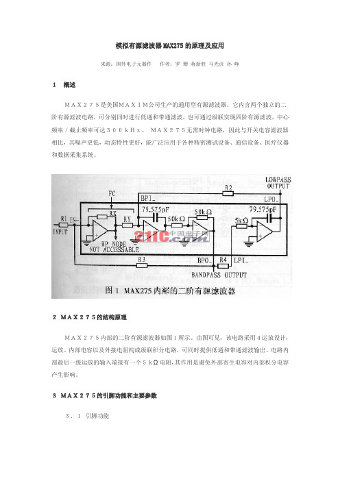
2MAX275的结构原理MAX275内部的二阶有源滤波器如图1所示。
由图可见,该电路采用4运放设计,运放、内部电容以及外接电阻构成级联积分电路,可同时提供低通和带通滤波输出。
电路内部最后一级运放的输入端接有一个5kΩ电阻,其作用是避免外部寄生电容对内部积分电容产生影响。
3MAX275的引脚功能和主要参数3.1引脚功能MAX275采用20脚DIP或SO封装形式,引脚排列如图2所示。
使用时只要根据相关公式计算出合适的外接电阻,经过简单的连接就能很好地满足设计要求。
其主要引脚的功能如下(内部的两个独立二阶有源滤波器分别用A、B表示):V+,V-,:正、负电源输入端。
INA,INB:信号输入端。
LPIA,LPIB:低通滤波输入端。
LPOA,LPOB:低通滤波输出端。
BPIA,BPIB:带通滤波输入端。
BPOA,BPOB:带通滤波输出端。
FCA,FCB:频率控制端。
3.2主要性能参数MAX275的主要性能参数如下:● 频率范围:100~300kHz;● 频率精度:±0.9%;● 频率精度温漂:-24ppm/℃;● Q值温漂:38ppm/℃;● 宽带噪声:6μVRMS(1Hz~10Hz),42μVRMS(10Hz~10kHz);● 失调电压:±125mV(低通输出),±50mV(带通输出);● 失调电压温漂:20μV/℃;● 谐波失真:-89dB(FTEST=1kHz),-83dB(FTEST=10kHz);● 输出电压摆幅:±4.5V(RL=5kΩ);● 电源电压范围:-2.37V~+5.50V;● 工作温度范围:-40℃~85℃。
max275 中文

海纳电子资讯网www.fpga-arm.com为您提供各种IC的应用
海纳电子资讯网www.fpga-arm.com为您提供各种IC的应用
海纳电子资讯网www.fpga-arm.com为您提供各种IC的应用
海纳电子资讯网www.fpga-arm.com为您提供各种IC的应用
海纳电子资讯网www.fpga-arm.com为您提供各种IC的应用
海纳电子资讯网www.fpga-arm.com为您提供各种IC的应用
海纳电子资讯网www.fpga-arm.com为您提供各种IC的应用
海纳电子资讯网www.fpga-arm.com为您提供各种IC的应用
海纳电子资讯网www.fpga-arm.com为您提供各种IC的应用
海纳电子资讯网www.fpga-arm.com为您提供各种IC的应用
海纳电子资讯网www.fpga-arm.com为您提供各种IC的应用
海纳电子资讯网www.fpga-arm.com为您提供各种IC的应用
海纳电子资讯网www.fpga-arm.com为您提供各种IC的应用
海纳电子资讯网www.fpga-arm.com为您提供各种IC的应用
海纳电子资讯网www.fpga-arm.com为您提供各种IC的应用
海纳电子资讯网www.fpga-arm.com为您提供各种IC的应用
海纳电子资讯网www.fpga-arm.com为您提供各种IC的应用
海纳电子资讯网www.fpga-arm.com为您提供各种IC的应用
海纳电子资讯网www.fpga-arm.com为您提供各种IC的应用
海纳电子资讯网www.fpga-arm.com为您提供各种Iarm.com为您提供各种IC的应用
海纳电子资讯网www.fpga-arm.com为您提供各种IC的应用
MAX3225EAAP+中文资料

________________General DescriptionThe MAX3224E/MAX3225E/MAX3226E/MAX3227E/MAX3244E/MAX3245E are 3V-powered EIA/TIA-232and V.28/V.24 communications interfaces with automat-ic shutdown/wakeup features, high data-rate capabili-ties, and enhanced electrostatic discharge (ESD)protection. All transmitter outputs and receiver inputs are protected to ±15kV using IEC 1000-4-2 Air-Gap Discharge, ±8kV using IEC 1000-4-2 Contact Discharge,and ±15kV using the Human Body Model.All devices achieve a 1µA supply current using Maxim’s revolutionary AutoShutdown Plus™ feature. These devices automatically enter a low-power shutdown mode when the RS-232 cable is disconnected or the transmitters of the connected peripherals are inactive,and the UART driving the transmitter inputs is inactive for more than 30 seconds. They turn on again when they sense a valid transition at any transmitter or receiv-er input. AutoShutdown Plus saves power without changes to the existing BIOS or operating system.The MAX3225E/MAX3227E/MAX3245E also feature MegaBaud™ operation, guaranteeing 1Mbps for high-speed applications such as communicating with ISDN modems. The MAX3224E/MAX3226E/MAX3244E guar-antee 250kbps operation. The transceivers have a pro-prietary low-dropout transmitter output stage enabling true RS-232 performance from a +3.0V to +5.5V supply with a dual charge pump. The charge pump requires only four small 0.1µF capacitors for operation from a 3.3V supply. The MAX3224E–MAX3227E feature a logic-level output (READY) that asserts when the charge pump is regulating and the device is ready to begin transmitting.All devices are available in a space-saving TQFN,SSOP, and TSSOP (MAX3224E/MAX3225E/MAX3244E/MAX3245E) packages.________________________ApplicationsNotebook, Subnotebook, and Palmtop Computers Cellular PhonesBattery-Powered Equipment Hand-Held Equipment Peripherals Printers__Next Generation Device Features♦For Space-Constrained Applications:MAX3228E/MAX3229E: ±15kV ESD-Protected,+2.5V to +5.5V, RS-232 Transceivers in UCSP MAX3222E/MAX3232E/MAX3241E †/MAX3246E:±15kV ESD-Protected, Down to 10nA, +3.0V to +5.5V, Up to 1Mbps, True RS-232 Transceivers (MAX3246E Available in UCSP™)♦For Low-Voltage or Data Cable Applications:MAX3380E/MAX3381E: +2.35V to +5.5V, 1µA,2Tx/2Rx RS-232 Transceivers with ±15kV ESD-Protected I/O and Logic PinsMAX3224E–MAX3227E/MAX3244E/MAX3245E †±15kV ESD-Protected, 1µA, 1Mbps, 3.0V to 5.5V ,RS-232 Transceivers with AutoShutdown Plus________________________________________________________________Maxim Integrated Products119-1339; Rev 9; 2/07Ordering Information continued at end of data sheet.*EP = Exposed paddle.†Covered by U.S. Patent numbers 4,636,930; 4,679,134; 4,777,577;4,797,899; 4,809,152; 4,897,774; 4,999,761; 5,649,210; and other patents pending.AutoShutdown Plus, MegaBaud, and UCSP are trademarks of Maxim Integrated Products, Inc.Ordering InformationFor pricing, delivery, and ordering information,please contact Maxim/Dallas Direct!at 1-888-629-4642, or visit Maxim’s website at .M A X 3224E –M A X 3227E /M A X 3244E /M A X 3245E †±15kV ESD-Protected, 1µA, 1Mbps, 3.0V to 5.5V ,RS-232 Transceivers with AutoShutdown PlusABSOLUTE MAXIMUM RATINGSELECTRICAL CHARACTERISTICS(V CC = +3V to +5.5V, C1–C4 = 0.1µF, tested at 3.3V ±10%; C 1= 0.047µF, C2–C4 = 0.33µF, tested at 5.0V ±10%; T A = T MIN to T MAX ,unless otherwise noted. Typical values are at T A = +25°C.)Stresses beyond those listed under “Absolute Maximum Ratings” may cause permanent damage to the device. These are stress ratings only, and functional operation of the device at these or any other conditions beyond those indicated in the operational sections of the specifications is not implied. Exposure to absolute maximum rating conditions for extended periods may affect device reliability.V CC to GND..............................................................-0.3V to +6V V+ to GND (Note 1)..................................................-0.3V to +7V V- to GND (Note 1)...................................................+0.3V to -7V V+ +⏐V-⏐(Note 1)................................................................+13V Input Voltages T_IN, FORCEON, FORCEOFF to GND................-0.3V to +6V R_IN to GND....................................................................±25V Output Voltages T_OUT to GND.............................................................±13.2V R_OUT, INVALID , READY to GND.........-0.3V to (V CC + 0.3V)Short-Circuit Duration T_OUT to GND.......................................................Continuous Continuous Power Dissipation (T A = +70°C)16-Pin SSOP (derate 7.14mW/°C above +70°C).........571mW 16-Pin TSSOP (derate 9.4mW/°C above +70°C)......754.7mW 16-Pin TQFN (derate 20.8mW/°C above +70°C)....1666.7mW20-Pin TQFN (derate 21.3mW/°C above +70°C)....1702.1mW 20-Pin Plastic DIP (derate 11.11mW/°C above +70°C)...889mW 20-Pin SSOP (derate 8.00mW/°C above +70°C).........640mW 20-Pin TSSOP (derate 10.9mW/°C above +70°C).......879mW 28-Pin Wide SO (derate 12.5mW/°C above +70°C)............1W 28-Pin SSOP (derate 9.52mW/°C above +70°C).........762mW 28-Pin TSSOP (derate 12.8mW/°C above +70°C).......1026mW 36-Pin TQFN (derate 26.3mW/°C above +70°C)...........2105mW Operating Temperature Ranges MAX32_ _EC_ _.................................................0°C to +70°C MAX32_ _EE_ _................................................-40°C to +85°C MAX32_ _EAA_..............................................-40°C to +125°C Storage Temperature Range.............................-65°C to +160°C Lead Temperature (soldering, 10s).................................+300°C Note 1:V+ and V- can have maximum magnitudes of 7V, but their absolute difference cannot exceed 13V.MAX3224E–MAX3227E/MAX3244E/MAX3245E †±15kV ESD-Protected, 1µA, 1Mbps, 3.0V to 5.5V ,RS-232 Transceivers with AutoShutdown Plus_______________________________________________________________________________________3ELECTRICAL CHARACTERISTICS (continued)(V CC = +3V to +5.5V, C1–C4 = 0.1µF, tested at 3.3V ±10%; C 1= 0.047µF, C2–C4 = 0.33µF, tested at 5.0V ±10%; T A = T MIN to T MAX ,unless otherwise noted. Typical values are at T A = +25°C.)M A X 3224E –M A X 3227E /M A X 3244E /M A X 3245E †±15kV ESD-Protected, 1µA, 1Mbps, 3.0V to 5.5V ,RS-232 Transceivers with AutoShutdown Plus 4_______________________________________________________________________________________TIMING CHARACTERISTICS—MAX3224E/MAX3226E/MAX3244E(V CC = +3V to +5.5V, C1–C4 = 0.1µF, tested at 3.3V ±10%; C 1= 0.047µF, C2–C4 = 0.33µF, tested at 5.0V ±10%; T A = T MIN to T MAX ,unless otherwise noted. Typical values are at T A = +25°C.)TIMING CHARACTERISTICS—MAX3225E/MAX3227E/MAX3245E(V CC = +3V to +5.5V, C1–C4 = 0.1µF, tested at 3.3V ±10%; C 1= 0.047µF, C2–C4 = 0.33µF, tested at 5.0V ±10%; T A = T MIN to T MAX ,unless otherwise noted. Typical values are at T= +25°C.)Note 3:Transmitter skew is measured at the transmitter zero cross points.MAX3224E–MAX3227E/MAX3244E/MAX3245E †±15kV ESD-Protected, 1µA, 1Mbps, 3.0V to 5.5V ,RS-232 Transceivers with AutoShutdown Plus_______________________________________________________________________________________5-6-5-4-3-2-10123456010002000300040005000MAX3224E/MAX3226ETRANSMITTER OUTPUT VOLTAGEvs. LOAD CAPACITANCELOAD CAPACITANCE (pF)T R A N S M I T T E R O U T P U T V O L T A G E (V )246810121416010002000300040005000MAX3224E/MAX3226ESLEW RATE vs. LOAD CAPACITANCELOAD CAPACITANCE (pF)S L E W R A T E (V /μs )5101520253035404520001000300040005000MAX3224E/MAX3226E OPERATING SUPPLY CURRENT vs. LOAD CAPACITANCELOAD CAPACITANCE (pF)S U P P L Y C U R R E N T (m A )-7.50-2.5-5.02.55.07.501000500150020002500MAX3225E/MAX3227ETRANSMITTER OUTPUT VOLTAGEvs. LOAD CAPACITANCELOAD CAPACITANCE (pF)T R A N S M I T T E R O U T P U T V O L T A G E (V )1510520253035404550010005001500200025003000MAX3225E/MAX3227E TRANSMITTER SKEW vs. LOAD CAPACITANCELOAD CAPACITANCE (pF)T R A N S M I T T E R S K E W (n s)807060504030201005001000150020002500MAX3225E/MAX3227ESLEW RATE vs. LOAD CAPACITANCELOAD CAPACITANCE (pF)S L E W R A T E (V /μs )2010403060507090801005001000150020002500MAX3225E/MAX3227E OPERATING SUPPLY CURRENT vs. LOAD CAPACITANCELOAD CAPACITANCE (pF)S U P P L Y C U R R E N T (m A )20242230282636343238-40020-20406080100MAX3224E–MAX3227E READY TURN-ON TIME vs. TEMPERATURETEMPERATURE (°C)R E A D Y T U R N -O N T I M E (μs )__________________________________________Typical Operating Characteristics(V CC = +3.3V, 250kbps data rate, 0.1µF capacitors, all transmitters loaded with 3k Ωand C L , T A = +25°C, unless otherwise noted.)20018016014012010080604020-40020-20406080100MAX3224E–MAX3227E READY TURN-OFF TIME vs. TEMPERATUREM A X 3224-7/44/45E -09TEMPERATURE (°C)R E A D Y T U R N -O F F T I M E (n s )M A X 3224E –M A X 3227E /M A X 3244E /M A X 3245E †±15kV ESD-Protected, 1µA, 1Mbps, 3.0V to 5.5V ,RS-232 Transceivers with AutoShutdown Plus 6____________________________________________________________________________________________________________________Typical Operating Characteristics (continued)(V CC = +3.3V, 250kbps data rate, 0.1µF capacitors, all transmitters loaded with 3k Ωand C L , T A = +25°C, unless otherwise noted.)-6-5-4-3-2-10123456010002000300040005000MAX3244ETRANSMITTER OUTPUT VOLTAGEvs. LOAD CAPACITANCELOAD CAPACITANCE (pF)T R A N S M I T T E R O U T P U T V O L T A G E (V )4286121014010002000300040005000MAX3244ESLEW RATE vs. LOAD CAPACITANCEM A X 3224-7/44/45E -11LOAD CAPACITANCE (pF)S L E W R A T E (V /μs )302010405060020001000300040005000MAX3244EOPERATING SUPPLY CURRENT vs. LOAD CAPACITANCELOAD CAPACITANCE (pF)S U P P L Y C U R R E N T (m A )-7.50-2.5-5.02.55.07.50800400120016002000MAX3245ETRANSMITTER OUTPUT VOLTAGEvs. LOAD CAPACITANCELOAD CAPACITANCE (pF)T R A N S M I T T E R O U T P U T V O L T A G E (V )2010403060507090801000400800120016002000MAX3245EOPERATING SUPPLY CURRENT vs. LOAD CAPACITANCELOAD CAPACITANCE (pF)S U P P L Y C U R R E N T (m A )201040306050700400800120016002000MAX3245ESLEW RATE vs. LOAD CAPACITANCELOAD CAPACITANCE (pF)S L E W R A T E (V /μs )1510520253035404550100020003000MAX3245E TRANSMITT SKEW vs. LOAD CAPACITANCEM A X 3224-7/44/45E -16LOAD CAPACITANCE (pF)T R A N S M I T T E R S K E W (n s )MAX3224E–MAX3227E/MAX3244E/MAX3245E †±15kV ESD-Protected, 1µA, 1Mbps, 3.0V to 5.5V ,RS-232 Transceivers with AutoShutdown Plus_______________________________________________________________________________________7M A X 3224E –M A X 3227E /M A X 3244E /M A X 3245E †±15kV ESD-Protected, 1µA, 1Mbps 3.0V to 5.5V ,RS-232 Transceivers with AutoShutdown Plus 8_______________________________________________________________________________________Dual Charge-Pump Voltage ConverterThe MAX3224E–MAX3227E/MAX3244E/MAX3245E’s internal power supply consists of a regulated dual charge pump that provides output voltages of +5.5V (doubling charge pump) and -5.5V (inverting charge pump), over the +3.0V to +5.5V range. The charge pump operates in discontinuous mode: if the output voltages are less than 5.5V, the charge pump ischarge-pump is disabled. Each charge pump requires a flying capacitor (C1, C2) and a reservoir capacitor (C3, C4) to generate the V+ and V- supplies.The READY output (MAX3224E–MAX3227E) is low when the charge pumps are disabled in shutdown mode. The READY signal asserts high when V- goes below -4V.MAX3224E–MAX3227E/MAX3244E/MAX3245E †±15kV ESD-Protected, 1µA, 1Mbps 3.0V to 5.5V ,RS-232 Transceivers with AutoShutdown Plus_______________________________________________________________________________________9RS-232 TransmittersThe transmitters are inverting level translators that convert CMOS-logic levels to 5.0V EIA/TIA-232 levels.The MAX3224E/MAX3226E/MAX3244E guarantee a 250kbps data rate (1Mbps, for the MAX3225E/MAX3227E/MAX3245E) with worst-case loads of 3k Ωin parallel with 1000pF, providing compatibility with PC-to-PC com-munication software (such as LapLink™). Transmitters can be paralleled to drive multiple receivers. Figure 1shows a complete system connection.When FORCEOFF is driven to ground or when the Auto-Shutdown Plus circuitry senses that all receiver and transmitter inputs are inactive for more than 30s, the transmitters are disabled and the outputs go into a high-impedance state. When powered off or shut down, the outputs can be driven to ±12V. The transmitter inputs do not have pullup resistors. Connect unused inputs to GND or V CC .Figure 1. Interface Under Control of PMUFigure 2. The MAX3244E/MAX3245E detect RS-232 activity when the UART and interface are shut down.LapLink is a trademark of Traveling Software.M A X 3224E –M A X 3227E /M A X 3244E /M A X 3245E †±15kV ESD-Protected, 1µA, 1Mbps 3.0V to 5.5V ,RS-232 Transceivers with AutoShutdown Plus 10______________________________________________________________________________________RS-232 ReceiversThe receivers convert RS-232 signals to CMOS-logic output levels. The MAX3224E–MAX3227E feature inverting outputs that always remain active (Table 1).The MAX3244E/MAX3245E have inverting three-state outputs that are high impedance when shut down (FORCEOFF = GND) (Table 1).The MAX3244E/MAX3245E feature an extra, always active, noninverting output, R2OUTB. R2OUTB output monitors receiver activity while the other receivers are high impedance, allowing ring indicator applications to be monitored without forward biasing other devices connected to the receiver outputs. This is ideal for sys-tems where V CC is set to ground in shutdown to accommodate peripherals such as UARTs (Figure 2).The MAX3224E–MAX3227E/MAX3244E/MAX3245E fea-ture an INVALID output that is enabled low when no valid RS-232 voltage levels have been detected on all receiver inputs. Because INVALID indicates the receiv-er input’s condition, it is independent of FORCEON and FORCEOFF states (Figures 3 and 4).AutoShutdown Plus ModeThe MAX3224E–MAX3227E/MAX3244E/MAX3245E achieve a 1µA supplycurrent with Maxim’s AutoShutdown Plus feature, which operates when FORCEOFF is high and a FORCEON is low. When these devices do not sense a valid signal transition on any receiver and trans-mitter input for 30s, the on-board charge pumps are shut down, reducing supply current to 1µA. This occurs if the RS-232 cable is disconnected or if the connectedTable 1. Output Control Truth TableX = Don’t care*INVALID connected to FORCEON**INVALID connected to FORCEON and FORCEOFFMAX3224E–MAX3227E/MAX3244E/MAX3245E †±15kV ESD-Protected, 1µA, 1Mbps 3.0V to 5.5V ,RS-232 Transceivers with AutoShutdown Plusperipheral transmitters are turned off, and the UART dri-ving the transmitter inputs is inactive. The system turns on again when a valid transition is applied to any RS-232 receiver or transmitter input. As a result, the sys-tem saves power without changes to the existing BIOS or operating system.Figures 3a and 3b depict valid and invalid RS-232receiver voltage levels. INVALID indicates the receiver input’s condition, and is independent of FORCEON and FORCEOFF states. Figure 3 and Tables 1 and 2 sum-marize the operating modes of the MAX3224E–MAX3227E/MAX3244E/MAX3245E. FORCEON and FORCEOFF override AutoShutdown Plus circuitry.When neither control is asserted, the IC selects between these states automatically based on the last receiver or transmitter input edge received.When shut down, the device’s charge pumps turn off,V+ is pulled to V CC , V- is pulled to ground, the transmit-ter outputs are high impedance, and READY (MAX3224E–MAX3227E) is driven low. The time required to exit shutdown is typically 100µs (Figure 8).By connecting FORCEON to INVALID , the MAX3224E–MAX3227E/MAX3244E/MAX3245E shut down when no valid receiver level and no receiver or transmitter edge is detected for 30s, and wake up when a valid receiver level or receiver or transmitter edge is detected.Figure 3a. INVALID Functional Diagram, INVALID Low Figure 3b. INVALID Functional Diagram, INVALID HighFigure 3c. AutoShutdown Plus LogicFigure 3d. Power-Down LogicFigure 4a. Receiver Positive/Negative Thresholds for INVALIDM A X 3224E –M A X 3227E /M A X 3244E /M A X 3245E †±15kV ESD-Protected, 1µA, 1Mbps 3.0V to 5.5V ,RS-232 Transceivers with AutoShutdown PlusBy connecting FORCEON and FORCEOFF to INVALID ,the MAX3224E–MAX3227E/MAX3244E/MAX3245E shut down when no valid receiver level is detected and wake up when a valid receiver level is detected (same functionality as AutoShutdown feature on MAX3221E/MAX3223E/MAX3243E).A mouse or other system with AutoShutdown Plus may need time to wake up. Figure 5 shows a circuit that forces the transmitters on for 100ms, allowing enough time for the other system to realize that the MAX3244E/MAX3245E is awake. If the other system outputs valid RS-232 signal transitions within that time, the RS-232ports on both systems remain enabled.Software-Controlled ShutdownIf direct software control is desired, use INVALID to indicate DTR or ring indicator signal. Tie FORCEOFF and FORCEON together to bypass the AutoShutdown Plus so the line acts like a SHDN input.±15kV ESD ProtectionAs with all Maxim devices, ESD-protection structures are incorporated on all pins to protect against electrostaticdischarges encountered during handling and assembly.The driver outputs and receiver inputs of the MAX3224E–MAX3227E/MAX3244E/MAX3245E have extra protection against static electricity. Maxim’s engineers have developed state-of-the-art structures to protectFigure 4b. AutoShutdown Plus, INVALID,and READY Timing DiagramFigure 5. AutoShutdown Plus Initial Turn-On to Wake Up a Mouse or Another SystemMAX3224E–MAX3227E/MAX3244E/MAX3245E †±15kV ESD-Protected, 1µA, 1Mbps 3.0V to 5.5V ,RS-232 Transceivers with AutoShutdown Plusthese pins against ESD of ±15kV without damage. The ESD structures withstand high ESD in all states: normal operation, shutdown, and powered down. After an ESD event, Maxim’s E versions keep working without latchup, whereas competing RS-232 products can latch and must be powered down to remove latchup.ESD protection can be tested in various ways; the transmitter outputs and receiver inputs of this product family are characterized for protection to the following limits:1)±15kV using the Human Body Model2)±8kV using the Contact-Discharge Method specified in IEC1000-4-23)±15kV using IEC1000-4-2’s Air-Gap Method.ESD Test ConditionsESD performance depends on a variety of conditions.Contact Maxim for a reliability report that documents test setup, test methodology, and test results.Human Body ModelFigure 6a shows the Human Body Model and Figure 6b shows the current waveform it generates when dis-charged into a low impedance. This model consists of a 100pF capacitor charged to the ESD voltage of inter-est, which is then discharged into the test device through a 1.5k Ωresistor.Figure 6b. Human Body Current WaveformFigure 7b. IEC1000-4-2 ESD Generator Current WaveformFigure 6a. Human Body ESD Test Model Figure 7a. IEC1000-4-2 ESD Test ModelM A X 3224E –M A X 3227E /M A X 3244E /M A X 3245E †±15kV ESD-Protected, 1µA, 1Mbps 3.0V to 5.5V ,RS-232 Transceivers with AutoShutdown Plus IEC1000-4-2The IEC1000-4-2 standard covers ESD testing and per-formance of finished equipment; it does not specifically refer to integrated circuits. The MAX3224E–MAX3227E,MAX3244E/MAX3245E help you design equipment that meets Level 4 (the highest level) of IEC1000-4-2, with-out the need for additional ESD-protection components.The major difference between tests done using the H uman Body Model and IEC1000-4-2 is higher peak current in IEC1000-4-2, because series resistance is lower in the IEC1000-4-2 model. Hence, the ESD with-stand voltage measured to IEC1000-4-2 is generally lower than that measured using the H uman Body Model. Figure 7a shows the IEC1000-4-2 model and Figure 7b shows the current waveform for the 8kV,IEC1000-4-2, Level 4, ESD Contact-Discharge Method.The Air-Gap Method involves approaching the device with a charged probe. The Contact-Discharge Method connects the probe to the device before the probe is energized.Machine ModelThe Machine Model for ESD tests all pins using a 200pF storage capacitor and zero discharge resis-tance. Its objective is to emulate the stress caused by contact that occurs with handling and assembly during manufacturing. Of course, all pins require this protec-tion during manufacturing, not just RS-232 inputs and outputs. Therefore, after PC board assembly, the Machine Model is less relevant to I/O ports.__________Applications InformationCapacitor SelectionThe capacitor type used for C1–C4 is not critical for proper operation; polarized or nonpolarized capacitorscan be used. The charge pump requires 0.1µF capaci-tors for 3.3V operation. For other supply voltages, see Table 3 for required capacitor values. Do not use val-ues smaller than those listed in Table 3. Increasing the capacitor values (e.g., by a factor of 2) reduces ripple on the transmitter outputs and slightly reduces power consumption. C2, C3, and C4 can be increased without changing C1’s value. However, do not increase C1without also increasing the values of C2, C3, C4,and C BYPASS , to maintain the proper ratios (C1 to the other capacitors).When using the minimum required capacitor values,make sure the capacitor value does not degrade excessively with temperature. If in doubt, use capaci-tors with a larger nominal value. The capacitor’s equiv-alent series resistance (ESR), which usually rises at low temperatures, influences the amount of ripple on V+and V-.Power-Supply DecouplingIn most circumstances, a 0.1µF V CC bypass capacitor is adequate. In applications that are sensitive to power-supply noise, use a capacitor of the same value as charge-pump capacitor C1. Connect bypass capaci-tors as close to the IC as possible.Transmitter Outputs when Exiting ShutdownFigure 8 shows two transmitter outputs when exiting shutdown mode. As they become active, the two trans-mitter outputs are shown going to opposite RS-232 lev-els (one transmitter input is high, the other is low). Each5μs/divV CC = 3.3V C1–C4 = 0.1μFFigure 8. Transmitter Outputs when Exiting Shutdown or Powering Uptransmitter is loaded with 3k Ωin parallel with 1000pF.The transmitter outputs display no ringing or undesir-able transients as they come out of shutdown. Note that the transmitters are enabled only when the magnitude of V- exceeds approximately -3V.High Data RatesThe MAX3224E/MAX3226E/MAX3244E maintain the RS-232 ±5.0V minimum transmitter output voltage even at high data rates. Figure 9 shows a transmitter loop-back test circuit. Figure 10 shows a loopback test result at 120kbps, and Figure 11 shows the same test at 250kbps. For Figure 10, all transmitters were driven simultaneously at 120kbps into RS-232 loads in parallel with 1000pF. For Figure 11, a single transmitter was dri-ven at 250kbps, and all transmitters were loaded with an RS-232 receiver in parallel with 250pF.The MAX3225E/MAX3227E/MAX3245E maintain the RS-232 ±5.0V minimum transmitter output voltage at data rates up to 1Mbps (MegaBaud). Figure 12 shows a loopback test result with a single transmitter driven at 1Mbps and all transmitters loaded with an RS-232receiver in parallel with 250pF.MAX3224E–MAX3227E/MAX3244E/MAX3245E †±15kV ESD-Protected, 1µA, 1Mbps 3.0V to 5.5V ,RS-232 Transceivers with AutoShutdown PlusFigure 9. Loopback Test CircuitFigure 10. MAX3224E/MAX3226E/MAX3244E Loopback Test Result at 120kbps2μs/divV CC = 3.3VFigure 11. MAX3224E/MAX3226E/MAX3244E Loopback Test Result at 250kbps2μs/divV CC = 3.3VFigure 12. MAX3225E/MAX3227E/MAX3245E Loopback Test Result at 1Mbps200ns/div5V/div5V/div5V/divV CC = 3.3VM A X 3224E –M A X 3227E /M A X 3244E /M A X 3245E †±15kV ESD-Protected, 1µA, 1Mbps 3.0V to 5.5V ,RS-232 Transceivers with AutoShutdown Plus Figure 13a. Mouse Driver Test CircuitMAX3224E–MAX3227E/MAX3244E/MAX3245E †±15kV ESD-Protected, 1µA, 1Mbps 3.0V to 5.5V ,RS-232 Transceivers with AutoShutdown PlusMouse DriveabilityThe MAX3244E/MAX3245E are specifically designed to power serial mice while operating from low-voltage power supplies. They have been tested with leading mouse brands from manufacturers such as Microsoft and Logitech. The MAX3244E/MAX3245E successfully drove all serial mice tested and met their respective current and voltage requirements. The MAX3244E/MAX3245E dual charge pump ensures the transmitters supply at least ±5V during worst-case conditions.Figure 13b shows the transmitter output voltages under increasing load current. Figure 13a shows a typical mouse connection.Interconnection with 3V and 5V LogicThe MAX3224E–MAX3227E/MAX3244E/MAX3245E can directly interface with various 5V logic families, includ-ing ACT and HCT CMOS. See Table 4 for more informa-tion on possible combinations of interconnections.Table 5 lists other Maxim ESD-powered transceivers.Table 5. ±15kV ESD-Protected, 3.0V to 5.5V Powered RS-232 Transceivers from MaximM A X 3224E –M A X 3227E /M A X 3244E /M A X 3245E †±15kV ESD-Protected, 1µA, 1Mbps 3.0V to 5.5V ,RS-232 Transceivers with AutoShutdown Plus___________________________________________________Typical Operating CircuitsMAX3224E–MAX3227E/MAX3244E/MAX3245E †±15kV ESD-Protected, 1µA, 1Mbps 3.0V to 5.5V ,RS-232 Transceivers with AutoShutdown Plus___________________________________________________________Pin ConfigurationsM A X 3224E –M A X 3227E /M A X 3244E /M A X 3245E †±15kV ESD-Protected, 1µA, 1Mbps 3.0V to 5.5V ,RS-232 Transceivers with AutoShutdown Plus ___________________________________________Ordering Information (continued)___________________Chip InformationMAX3224E TRANSISTOR COUNT: 1129MAX3225E TRANSISTOR COUNT: 1129MAX3226E TRANSISTOR COUNT: 1129MAX3227E TRANSISTOR COUNT: 1129MAX3244E/MAX3245E TRANSISTOR COUNT: 1335PROCESS: BICMOS*EP = Exposed paddle.MAX3224E–MAX3227E/MAX3244E/MAX3245E †±15kV ESD-Protected, 1µA, 1Mbps 3.0V to 5.5V ,RS-232 Transceivers with AutoShutdown Plus______________________________________________________________________________________21Package Information(The package drawing(s) in this data sheet may not reflect the most current specifications. For the latest package outline information,go to /packages .)。
MPX 275VAC承认书

12
Dry Heat Resistance
Insulation Resistance 量 率 Capacitance Variation
Temperature: +100 Duration: 96 4 hrs
2°C
Appearance
Withstand Voltage
13
Humidity Resistance
5 6
量 Capacitance 數 Dissipation Factor 拉 度 Pull Strength
Within specified tolerance 0.1 %max at 1KHz
7
度 Terminal Strength
不 No cutting or slack of terminals 度 Bending Strength 異 No abnormality of the appearance 95% At least 95% of the surface of the lead wire dipped into is covered with new solder. 異 No abnormality on appearance 3 Comply with item 3 3%
Charge time: 60 5sec. Charge voltage: 100VDC Test Temp: 25°C at 1 KHz 10% Measure R.V: 5 Vrms or below Test temp: 25°C Measure R.V: 5 Vrms or below Test temp: 25°C Wire diameter: 0.6&0.8 mm Load: 1 kg, time: 10 sec. Wire diameter: 1.0 mm Load: 2 kg, time: 20 sec. Wire diameter: 0.6&0.8 mm Load: 0.5 kg, 90° x 4 time Wire diameter: 1.0 mm Load: 1 kg, 90° x 4 time Frequency range 10-55-10 Hz Amplitude: 1.5 mm, 2 hrs/direction for 3 directions Solder temp: 240 2°C Immersion time: 2 0.5sec. Solder: SnAgCu (Sn:96.5% Ag:3% Cu:0.5%)