90156-0142中文资料
12061A391FAT2A中文资料

4% ⌬ C a p a c i t a n c eTemperature °CTemperature CoefficientI m p e d a n c e , ⍀Frequency, MHzVariation of Impedance with Chip SizeImpedance vs. Frequency 1000 pF - C0G (NP0)% ⌬ C a p a c i t a n c eFrequency⌬ Capacitance vs. FrequencyI m p e d a n c e , ⍀Frequency, MHzVariation of Impedance with Cap ValueImpedance vs. Frequency0805 - C0G (NP0)10 pF vs. 100 pF vs. 1000 pFGeneral SpecificationsC0G (NP0) is the most popular formulation of the “temperature-compensating,” EIA Class I ceramic materials.Modern C0G (NP0) formulations contain neodymium,samarium and other rare earth oxides.C0G (NP0) ceramics offer one of the most stable capacitor dielectrics available. Capacitance change with temperature is 0 ±30ppm/°C which is less than ±0.3% ⌬C from -55°C to +125°C. Capacitance drift or hysteresis for C0G (NP0)ceramics is negligible at less than ±0.05% versus up to ±2% for films. Typical capacitance change with life is less than ±0.1% for C0G (NP0), one-fifth that shown by most other dielectrics. C0G (NP0) formulations show no aging characteristics.0805Size (L" x W")5Voltage 6.3V = 610V = Z 16V = Y 25V = 350V = 5100V = 1200V = 2500V = 7ADielectric C0G (NP0) = A101Capacitance Code (In pF)2 Sig. Digits +Number of ZerosJCapacitance T olerance B =±.10 pF (<10pF)C =±.25 pF (<10pF)D =±.50 pF (<10pF)F =±1% (≥ 10 pF)G =±2% (≥ 10 pF)J =±5%K =±10%AFailure Rate A = Not ApplicableT Terminations T = Plated Niand Sn7 = Gold Plated2Packaging2 = 7" Reel 4 = 13" Reel 7 = Bulk Cass.9 = BulkContact Factory For MultiplesASpecial Code A = Std. ProductPART NUMBER (see page 2 for complete part number explanation)Contact Factory For 1 = Pd/Ag TermNOTE: Contact factory for availability of T ermination and T olerance Options for Specific Part Numbers.Contact factory for non-specified capacitance values.Specifications and Test Methods5PREFERRED SIZES ARE SHADED67。
S-80950中文资料

Features
• Ultra-low current consumption 1.0 µA typ. (VDD=2.0 V) ; Products with a detection voltage of 1.4V or less 1.2 µA typ. (VDD=3.5 V) ; Products with a detection voltage of 1.5V or more • High-precision detection voltage ±2.0% • Low operating voltage 0.80 to 6.0 V ; Products with detection voltage of 1.4‚uor less
SOT-23-5 Top view
5 4 1 OUT 2 VDD 3 VSS 4 NC 1 2 3 5 CD
Pin Assignment
Figure 1
Block Diagram
(1) Nch open-drain active low output (2) CMOS active low output
Table 1
Detection voltage range (V) 1.1V±2.0% 1.2V±2.0% 1.3V±2.0% 1.4V±2.0% 1.5V±2.0% 1.6V±2.0% 1.7V±2.0% 1.8V±2.0% 1.9V±2.0% 2.0V±2.0% 2.1V±2.0% 2.2V±2.0% 2.3V±2.0% 2.4V±2.0% 2.5V±2.0% 2.6V±2.0% 2.7V±2.0% 2.8V±2.0% 2.9V±2.0% 3.0V±2.0% 3.1V±2.0% 3.2V±2.0% 3.3V±2.0% 3.4V±2.0% 3.5V±2.0% 3.6V±2.0% 3.7V±2.0% 3.8V±2.0% 3.9V±2.0% 4.0V±2.0% 4.1V±2.0% 4.2V±2.0% 4.3V±2.0% 4.4V±2.0% 4.5V±2.0% 4.6V±2.0% 4.7V±2.0% 4.8V±2.0% 4.9V±2.0% 5.0V±2.0% 5.1V±2.0% 5.2V±2.0% 5.3V±2.0% 5.4V±2.0% 5.5V±2.0% 5.6V±2.0% 5.7V±2.0% 5.8V±2.0% 5.9V±2.0% 6.0V±2.0% Hysteresis width VHYS typ.(V) 0.055 0.060 0.065 0.070 0.075 0.080 0.085 0.090 0.095 0.100 0.105 0.110 0.115 0.120 0.125 0.130 0.135 0.140 0.145 0.150 0.155 0.160 0.165 0.170 0.175 0.180 0.185 0.190 0.195 0.200 0.205 0.210 0.215 0.220 0.225 0.230 0.235 0.240 0.245 0.250 0.255 0.260 0.265 0.270 0.275 0.280 0.285 0.290 0.295 0.300 Nch Open Drain(Low) S-80911ANMP-D71-T2 S-80912ANMP-D72-T2 S-80913ANMP-DDA-T2 S-80914ANMP-DDB-T2 S-80915ANMP-DDC-T2 S-80916ANMP-DDD-T2 S-80917ANMP-DDE-T2 S-80918ANMP-DDF-T2 S-80919ANMP-DDG-T2 S-80920ANMP-DDH-T2 S-80921ANMP-DDJ-T2 S-80922ANMP-DDK-T2 S-80923ANMP-DDL-T2 S-80924ANMP-DDM-T2 S-80925ANMP-DDN-T2 S-80926ANMP-DDP-T2 S-80927ANMP-DDQ-T2 S-80928ANMP-DDR-T2 S-80929ANMP-DDS-T2 S-80930ANMP-DDT-T2 S-80931ANMP-DDV-T2 S-80932ANMP-DDW-T2 S-80933ANMP-DDX-T2 S-80934ANMP-DDY-T2 S-80935ANMP-DDZ-T2 S-80936ANMP-DD0-T2 S-80937ANMP-DD1-T2 S-80938ANMP-DD2-T2 S-80939ANMP-DD3-T2 S-80940ANMP-DD4-T2 S-80941ANMP-DD5-T2 S-80942ANMP-DD6-T2 S-80943ANMP-DD7-T2 S-80944ANMP-DD8-T2 S-80945ANMP-DD9-T2 S-80946ANMP-DJA-T2 S-80947ANMP-DJB-T2 S-80948ANMP-DJC-T2 S-80949ANMP-DJD-T2 S-80950ANMP-DJE-T2 S-80951ANMP-DJF-T2 S-80952ANMP-DJG-T2 S-80953ANMP-DJH-T2 S-80954ANMP-DJJ-T2 S-80955ANMP-DJK-T2 S-80956ANMP-DJL-T2 S-80957ANMP-DJM-T2 S-80958ANMP-DJN-T2 S-80959ANMP-DJP-T2 S-80960ANMP-DJQ-T2 CMOS Output(Low) S-80911ALMP-D51-T2 S-80912ALMP-D52-T2 S-80913ALMP-DAA-T2 S-80914ALMP-DAB-T2 S-80915ALMP-DAC-T2 S-80916ALMP-DAD-T2 S-80917ALMP-DAE-T2 S-80918ALMP-DAF-T2 S-80919ALMP-DAG-T2 S-80920ALMP-DAH-T2 S-80921ALMP-DAJ-T2 S-80922ALMP-DAK-T2 S-80923ALMP-DAL-T2 S-80924ALMP-DAM-T2 S-80925ALMP-DAN-T2 S-80926ALMP-DAP-T2 S-80927ALMP-DAQ-T2 S-80928ALMP-DAR-T2 S-80929ALMP-DAS-T2 S-80930ALMP-DAT-T2 S-80931ALMP-DAV-T2 S-80932ALMP-DAW-T2 S-80933ALMP-DAX-T2 S-80934ALMP-DAY-T2 S-80935ALMP-DAZ-T2 S-80936ALMP-DA0-T2 S-80937ALMP-DA1-T2 S-80938ALMP-DA2-T2 S-80939ALMP-DA3-T2 S-80940ALMP-DA4-T2 S-80941ALMP-DA5-T2 S-80942ALMP-DA6-T2 S-80943ALMP-DA7-T2 S-80944ALMP-DA8-T2 S-80945ALMP-DA9-T2 S-80946ALMP-DEA-T2 S-80947ALMP-DEB-T2 S-80948ALMP-DEC-T2 S-80949ALMP-DED-T2 S-80950ALMP-DEE-T2 S-80951ALMP-DEF-T2 S-80952ALMP-DEG-T2 S-80953ALMP-DEH-T2 S-80954ALMP-DEJ-T2 S-80955ALMP-DEK-T2 S-80956ALMP-DEL-T2 S-80957ALMP-DEM-T2 S-80958ALMP-DEN-T2 S-80959ALMP-DEP-T2 S-80960ALMP-DEQ-T2
AO4704中文资料

AO4704AO4704SymbolTyp Max 28405475R θJL 2130SymbolTyp Max 36406775R θJL 2530Maximum Junction-to-LeadCSteady-State°C/WParameterUnits Maximum Junction-to-AmbientAt ≤ 10s R θJA °C/W Maximum Junction-to-AmbientASteady-State °C/W °C/W Maximum Junction-to-AmbientASteady-State Thermal Characteristics: Schottky Maximum Junction-to-Lead CSteady-State°C/WThermal Characteristics ParameterUnits Maximum Junction-to-AmbientAt ≤ 10s R θJA °C/W A: The value of R θJA is measured with the device mounted on 1in 2 FR-4 board with 2oz. Copper, in a still air environment with T A =25°C. The value in any given application depends on the user's specific board design. The current rating is based on the t ≤ 10s thermal resistance rating.B: Repetitive rating, pulse width limited by junction temperature.C. The R θJA is the sum of the thermal impedence from junction to lead R θJL and lead to ambient.D. The static characteristics in Figures 1 to 6 are obtained using 80 µs pulses, duty cycle 0.5% max.E. These tests are performed with the device mounted on 1 in 2 FR-4 board with 2oz. Copper, in a still air environment with T A =25°C. The SOA curve provides a single pulse rating.F. The Schottky appears in parallel with the MOSFET body diode, even though it is a separate chip. Therefore, we provide the net forward drop, capacitance and recovery characteristics of the MOSFET and Schottky. However, the thermal resistance is specified for each chip separately.Rev5: August 2005THIS PRODUCT HAS BEEN DESIGNED AND QUALIFIED FOR THE CONSUMER MARKET. APPLICATIONS OR USES AS CRITICAL COMPONENTS IN LIFE SUPPORT DEVICES OR SYSTEMS ARE NOT AUTHORIZED. AOS DOES NOT ASSUME ANY LIABILITY ARISINGOUT OF SUCH APPLICATIONS OR USES OF ITS PRODUCTS. AOS RESERVES THE RIGHT TO IMPROVE PRODUCT DESIGN,FUNCTIONS AND RELIABILITY WITHOUT NOTICE.AO4704SymbolMin TypMaxUnits BV DSS 30V0.0070.053.2101220I GSS 100nA V GS(th)0.6 1.12V I D(ON)40A 9.111.5T J =125°C13.316.510.513m Ωg FS 3037S V SD 0.450.5V I S5A DYNAMIC PARAMETERS C iss 36564050pF C oss 322pF C rss 168pF R g0.86 1.1ΩSWITCHING PARAMETERS Q g (4.5V)30.536nC Q gs 4.6nC Q gd 8.6nC t D(on) 6.29ns t r 4.87ns t D(off)5575ns t f 7.311ns t rr 20.325ns Q rr8.412.5nCTHIS PRODUCT HAS BEEN DESIGNED AND QUALIFIED FOR THE CONSUMER MARKET. APPLICATIONS OR USES AS CRITICAL COMPONENTS IN LIFE SUPPORT DEVICES OR SYSTEMS ARE NOT AUTHORIZED. AOS DOES NOT ASSUME ANY LIABILITY ARISING OUT OF SUCH APPLICATIONS OR USES OF ITS PRODUCTS. AOS RESERVES THE RIGHT TO IMPROVE PRODUCT DESIGN,FUNCTIONS AND RELIABILITY WITHOUT NOTICE.Gate resistanceGate Drain Charge Body Diode+Schottky Reverse Recovery ChargeI F =13A, dI/dt=100A/µsBody Diode+Schottky Reverse Recovery Time Turn-Off DelayTime V GS =10V, V DS =15V, R L =1.1Ω, R GEN =0ΩTurn-Off Fall TimeTotal Gate Charge Gate Source Charge I F =13A, dI/dt=100A/µs On state drain currentForward TransconductanceDiode + Schottky Forward Voltage I S =1A,V GS =0VV GS =4.5V, V DS =5V Turn-On DelayTime V GS =10V, V DS =15V, I D =13AV GS =0V, V DS =0V, f=1MHzTurn-On Rise Time Electrical Characteristics (T J =25°C unless otherwise noted)STATIC PARAMETERS Parameter Conditions I DSS mA Gate Threshold Voltage Drain-Source Breakdown Voltage I D =250µA, V GS =0VZero Gate Voltage Drain Current.(Set by Schottky leakage)Gate-Body leakage current V DS =V GS I D =250µA V R =30VV DS =0V, V GS = ±12V R DS(ON)Static Drain-Source On-Resistancem ΩV GS =4.5V, I D =12.2AV GS =10V, ID=13AV R =30V, T J =125°CV R =30V, T J =150°C Reverse Transfer Capacitance V DS =5V, I D =13AOutput Capacitance (FET+Schottky)Maximum Body-Diode + Schottky Continuous CurrentV GS =0V, V DS =15V, f=1MHz Input Capacitance A: The value of R θJA is measured with the device mounted on 1in 2 FR-4 board with 2oz. Copper, in a still air environment with T A =25°C. The value in any given application depends on the user's specific board design. The current rating is based on the t ≤ 10s thermal resistance rating.B: Repetitive rating, pulse width limited by junction temperature.C. The R θJA is the sum of the thermal impedence from junction to lead R θJL and lead to ambient.D. The static characteristics in Figures 1 to 6 are obtained using 80 µs pulses, duty cycle 0.5% max.E. These tests are performed with the device mounted on 1 in 2 FR-4 board with 2oz. Copper, in a still air environment with T A =25°C. The SOA curve provides a single pulse rating.F. The Schottky appears in parallel with the MOSFET body diode, even though it is a separate chip. Therefore, we provide the net forward drop, capacitance and recovery characteristics of the MOSFET and Schottky. However, the thermal resistance is specified for each chip separately Rev5: August 2005.AO4704AO4704。
0460121142;中文规格书,Datasheet资料
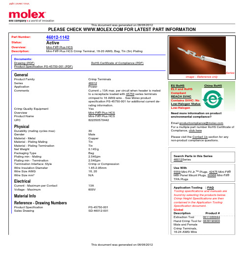
This document was generated on 08/08/2012PLEASE CHECK FOR LATEST PART INFORMATIONPart Number:46012-1142Status:ActiveOverview:Mini-Fit® Plus HCSDescription:Mini-Fit® Plus HCS Crimp Terminal, 18-20 AWG, Bag, Tin (Sn) PlatingDocuments:Drawing (PDF)RoHS Certificate of Compliance (PDF)Product Specification PS-45750-001 (PDF)GeneralProduct Family Crimp Terminals Series46012Application PowerCommentsCurrent = 13A max. per circuit when header is mated to a receptacle loaded with 45750 series terminals crimped to 16 AWG wire. . See Molex productspecification PS-45750-001 for additional current de-rating information.Crimp Quality Equipment YesOverviewMini-Fit® Plus HCS Product Name Mini-Fit® Plus HCS UPC822350570442PhysicalDurability (mating cycles max)30GenderMale Material - MetalCopper Material - Plating MatingTin Material - Plating Termination Tin Net Weight0.145/g Packaging Type BagPlating min - Mating2.540µm Plating min - Termination 2.540µmTermination Interface: Style Crimp or Compression Wire Insulation Diameter 1.65-2.95mm Wire Size AWG 18, 20Wire Size mm²N/A ElectricalCurrent - Maximum per Contact 13A Voltage - Maximum600VMaterial InfoReference - Drawing NumbersProduct Specification PS-45750-001Sales DrawingSD-46012-001Seriesimage - Reference onlyEU RoHSChina RoHSELV and RoHS Compliant REACH SVHCContains SVHC: No Low-Halogen Status Low-HalogenNeed more information on product environmental compliance?Email productcompliance@For a multiple part number RoHS Certificate of Compliance, click herePlease visit the Contact Us section for any non-product compliance questions.Search Parts in this Series 46012SeriesUse With5559 Mini-Fit Jr.™ Plugs, 42475 Mini-Fit®MBI Panel Mount Plugs, 30068 Mini-Fit®TPA PlugsApplication Tooling | FAQTooling specifications and manuals are found by selecting the products below.Crimp Height Specifications are then contained in the Application Tooling Specification document.GlobalDescription Product #Extraction Tool 0011030044Hand Crimp Tool for Male and Female Crimp Terminals,16-24 AWG Wire0638190900This document was generated on 08/08/2012PLEASE CHECK FOR LATEST PART INFORMATION分销商库存信息: MOLEX 0460121142。
1-1609115-7中文资料

Smallest Filtered Power Entry Modules with Metric FuseholdersThe GG series power entry modules combine the functionsofa general purpose RFI filter with an IEC power cord connector and single or dual metric fusing, in the smallest possible panel space. A choice of .250” terminals or wire leads is available for the load-side terminations.For maximum cost effectiveness, 6 amp models should be used for all applications rated 6 amps or less, unless the higher performance of the 3 amp models, or the much higher performance of the 1 amp models, is needed.Models with C-suffix additionally incorporate a ground choke 1to isolate the equipment chassis from external ground at RF frequencies.HG SeriesA medical version of our GG series, these filters offer the same compact design but reduce the line-to-ground capacitance in order to meet UL 2601 patient care requirements. For more information on UL2601 specification, see Appendix C.Note: When using the models with an IEC connector,remember that the leakage current of the companion line cord, GA400, is more significant than that of the filter -which may disqualify this line cord from use in patient care applications.SpecificationsMaximum leakage current,each line-to-groundHG ModelsGG Models @120 VAC 60 Hz:2µA .25 mA @250 VAC 50 Hz:5µA .42 mA Hipot rating (one minute):line-to-ground 1550 VAC line-to-line1450 VDC Operating frequency: 50/60 Hz Rated voltage (max.):250 VACFuse (not included):Accepts one 5x20mm fuse (-1 models) or two 5 x 20 mmfuses (-2 models)Minimum insertion loss in dB:Line-to-ground in 50 ohm circuit CurrentFrequency-MHz Rating .01.05.10.15.5151030GG/GS Models 1A 1223293241475050553A –10151930364850536A–14101622364050HG Models 1A 1223293240402822183A –10151925262221216A –410141818141414Line-to-line in 50 ohm circuit Current Frequency-MHz Rating.01.15.51351030GG/GS Models 1A 131423414750443A 121114253844406A12101323333942HG Models 1A 132635353527203A 123030303030306A12303030303030112GG/HG SeriesGG SeriesHG1/GG1GG8Electrical SchematicsGG-CLINENote 1Note 2LOADLINENote 1Note 2LOADResistor location for reference only.Note 1: Depicts single fuse for -1 models.Note 2: For HG delete line-to-ground capacitors.CAUTION: DO NOT ATTEMPT TO OPERATE A SINGLE-FUSED MODEL WITHOUT THE FUSE DOOR IN PLACE!UL Recognized CSA Certified VDE ApprovedSmallest Filtered Power Entry Modules with Metric Fuseholders(Continued) Case StylesCase DimensionsA B C D E±.015Part No.(max)(max)(max)(max)±.38EGG1-1/EGG1-2/ 2.15 1.13 1.29 1.417 1.76 EHG1-254.528.732.836.044.7 EGG8-1/EGG8-2 2.02 1.13 1.29 1.417 1.76 EGG8C-1/EGG8C-251.128.732.836.044.7 EGS1-1/EGS1-2 2.13 1.13 1.28 1.46* 1.42 EHGS1-254.028.732.536.036.1 EGG1C-1-1/EGG1C-2 2.45 1.13 1.28 1.46* 1.4262.2328.732.536.036.1*max113Power Entry ModulesGG/HG SeriesGG1/HG1GG8EGSBCADERecommended Panel Cutouts1.1429.01.41736.01.3033.0GG / HGFront or Back MountGS / HGSFront Mount Only1.2431.51.2932.8Typical dimensions:Terminals: .250 [6.35](3)Holes: .07 [1.8]Dia.Mounting Holes: .126 [3.20]Dia. (2)Typical dimensions:Wire leads: 5.0 [127.0]Min. 18 AWG Mounting Holes: .126 [3.20]Dia. (2)Part Number1RFI Filter Type2Current Rating3Metric Fuseholders Load Side Terminations1EGG1-1General Purpose211.250 [6.35]Terminals (3)1EGG1-2General Purpose12.250 [6.35]Terminals (3)1EGG8-1General Purpose11 5.0 [127.0]Wire Leads1EGG8-2General Purpose12 5.0 [127.0]Wire Leads1EGS1-1General Purpose11.250 [6.35]Terminals (3)1EGS1-2General Purpose12.250 [6.35]Terminals (3)3EGG1-1General Purpose31.250 [6.35]Terminals (3)3EGG1-2General Purpose32.250 [6.35]Terminals (3)3EGG8-1General Purpose31 5.0 [127.0]Wire Leads3EGG8-2General Purpose32 5.0 [127.0]Wire Leads3EGS1-1General Purpose31.250 [6.35]Terminals (3)3EGS1-2General Purpose32.250 [6.35]Terminals (3)6EGG1-1General Purpose61.250 [6.35]Terminals (3)6EGG1-2General Purpose62.250 [6.35]Terminals (3)6EGG8-1General Purpose61 5.0 [127.0]Wire Leads6EGG8-2General Purpose62 5.0 [127.0]Wire Leads6EGS1-1General Purpose61.250 [6.35]Terminals (3)6EGS1-2General Purpose62.250 [6.35]Terminals (3)1EHG1-2Medical12.250 [6.35]Terminals (3)3EHG1-2Medical32.250 [6.35]Terminals (3)6EHG1-2Medical62.250 [6.35]Terminals (3)1EHGS1-2Medical12.250 [6.35]Terminals (3)3EHGS1-2Medical32.250 [6.35]Terminals (3)6EHGS1-2Medical62.250 [6.35]Terminals (3)1Ground choke available on general purpose models. Add suffix "C" (1EGG1C-1). Does not include EGS models.2General purpose filter for susceptibility applications. 3Current rating @120 VAC and 250 VAC.for panel thickness.032-.080[.81-2.03]Radius: 0.138[0.35]。
RYII中文资料
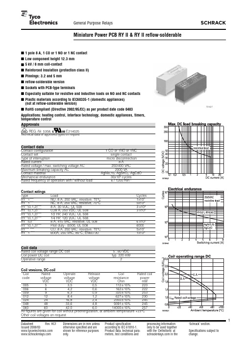
1Datasheet Rev. HC1 Issued 2008/03 Dimensions are in mm unlessotherwise specified and areshown for reference purposesProduct specificationaccording to IEC61810-1.Product data, technical para-processing informationonly to be used togetherwith the'Definitions' at‘Schrack’ section.Specifications subject toEspecially suitable for resistive and inductive loads on NO and NC contactsRoHS compliant (Directive 2002/95/EC) as per product date code 0403Applications: heating control, interface technology, domestic appliances, timers,V REG.-Nr. 5358, Z E214025Contact dataContact configuration 1 CO or 1NO or 1NCContact set single contactType of interruption micro disconnectionRated current8ARated voltage/max. switching voltage AC250/400VACMaximum breaking capacity AC2000VAContact material AgNi0,15, AgSnO2, AgCdOMechanical endurance30x106cyclesRated frequency of operation with/without load 6 / 1200min-1Contact ratingsType Load CyclesRY**1***NO, 8 A, 250 VAC, resistive, 70°C1x105RY**1***NC, 8 A, 250 VAC, resistive, 70°C5x104RY**(0,1,2)***8 A, 30 VDC, UL 5083x104RY**(0,1,2)***0,28 A, 250 VDC, UL 5083x104RY**(0,1,2)***1/2 HP, 240 VDC, UL 508RY**(0,1,2)***1/4 HP, 120 VDC, UL 508RY**(0)***8 A, 415 VAC, resistive, UL 5086x103RY**(0,1,2)***Pilot duty - B300, UL 5086000RY*** ***CO, 8 A, 250 VAC, resistive, 70°C5x103RY**1 ***6(4)A, 250 VAC, 85°C, EN607301x105Coil dataRated coil voltage range DC coil 5...60VDCCoil power DC coil typ. 220mWOperative range2Coil versions,DC-coilCoil Rated Operate Release Coil Rated coilcode voltage voltage voltage resistance powerVDC VDC VDC Ohm mW00553,50,5112+10%22300664,20,6162+10%22200996,30,9320+10%253012128,41,2627+10%2300242416,82,42350+10%2450484833,64,89391+10%2450606042,06,014000+10%257All figures are given for coil without preenergization, at ambient temperature +23°COther coil voltages on requestF0142-FInsulation CO contact NO contact Dielectric strength coil-contact circuit5000V effopen contact circuit1000V effClearance/creepage coil-contact circuit W8 / 8mmMaterial group of insulation parts IIIaTracking index of relay base PTI250, PTI 175* Type of insulation coil-contact circuit reinforcedopen contact circuit functionalRated insulation voltage250V250VPollution degree 3 23Rated voltage system230V 400V230 / 400VOvervoltage category III IIIOther dataRoHS - Directive 2002/95/EC compliant as per product date code 0403 Flammability class according to UL94V-0GWT to IEC 60335-1> 750 °C**Ambient temperature range -40...+70°CAmbient temperature max.85°C at 6AOperate- / release time typ. 7 / 3msBounce time NO / NC contact typ. 2.5 / 4.5ms Vibration resistance (function) NO/NC contact20 / 5gShock resistance (function) NO/NC contact20 / 5gShock resistance (destruction) 100gCategory of protection RTII-flux proof, RTIII- wash tight** Mounting pcbMounting position anyMinimum mounting distance W 0mmSoldering heat resistance flux proof version270°C/10swash tight version260°C/5sRelay weight8gPackaging unit20 / 500pcs AccessoiresFor technical details see datasheet Accessoires RYII* reflow-solderable version** not as reflow-solderable version PCB layout / terminal assignment Bottom view on solder pins1 NO, 1 NC contact 5mmS0254-AAS0254-ABS0254-ACS0254-ADS0254-AFS0254-AEDimensionsPinning 3.2mmPinning 5mmSoldering profile for reflow-solderable version。
AO4459中文资料

AO4459中⽂资料SymbolTyp Max 33406275R θJL 1824Maximum Junction-to-Lead CSteady-State°C/WThermal Characteristics ParameterUnits Maximum Junction-to-AmbientAt ≤ 10s R θJA °C/W Maximum Junction-to-Ambient ASteady-State °C/W AO4459AO4459SymbolMin TypMaxUnits BV DSS -30V -1T J =55°C-5I GSS ±100nA V GS(th)-1.5-1.85-2.5V I D(ON)-30A 3846T J =125°C53685872m ?g FS 11S V SD -0.78-1V I S-3.5A C iss 668830pF C oss 126pF C rss 92pF R g69?Q g (10V)12.716nC Q g (4.5V) 6.4nC Q gs 2nC Q gd 4nC t D(on)7.7ns t r 6.8ns t D(off)20ns t f 10ns t rr 2230ns Q rr15nCTHIS PRODUCT HAS BEEN DESIGNED AND QUALIFIED FOR THE CONSUMER MARKET. APPLICATIONS OR USES AS CRITICAL COMPONENTS IN LIFE SUPPORT DEVICES OR SYSTEMS ARE NOT AUTHORIZED. AOS DOES NOT ASSUME ANY LIABILITY ARISING OUT OF SUCH APPLICATIONS OR USES OF ITS PRODUCTS. AOS RESERVES THE RIGHT TO IMPROVE PRODUCT DESIGN,FUNCTIONS AND RELIABILITY WITHOUT NOTICE.DYNAMIC PARAMETERS Maximum Body-Diode Continuous CurrentGate resistanceV GS =0V, V DS =0V, f=1MHzV GS =0V, V DS =-15V, f=1MHz Input Capacitance Output Capacitance Turn-On Rise Time Turn-Off DelayTime V GS =-10V, V DS =-15V, R L =2.5?, R GEN =3?Turn-Off Fall TimeTurn-On DelayTime SWITCHING PARAMETERSTotal Gate Charge (4.5V)Gate Source Charge Gate Drain Charge Total Gate Charge (10V)V GS =-10V, V DS =-15V, I D =-6.5Am ?V GS =-4.5V, I D =-5AI S =-1A,V GS =0V V DS =-5V, I D =-6.5AR DS(ON)Static Drain-Source On-ResistanceForward TransconductanceDiode Forward VoltageI DSS µA Gate Threshold Voltage V DS =V GS I D =-250µA V DS =-24V, V GS =0VV DS =0V, V GS =±20V Zero Gate Voltage Drain Current Gate-Body leakage current Electrical Characteristics (T J =25°C unless otherwise noted)STATIC PARAMETERS ParameterConditions Body Diode Reverse Recovery Time Body Diode Reverse Recovery ChargeI F =-6.5A, dI/dt=100A/µsDrain-Source Breakdown Voltage On state drain currentI D =-250µA, V GS =0V V GS =-10V, V DS =-5V V GS =-10V, I D =-6.5AReverse Transfer Capacitance I F =-6.5A, dI/dt=100A/µs A: The value of R θJA is measured with the device mounted on 1in 2FR-4 board with 2oz. Copper, in a still air environment with T A =25°C. The value in any a given application depends on the user's specific board design. The current rating is based on the t ≤ 10s thermal resistance rating.B: Repetitive rating, pulse width limited by junction temperature.C. The R θJA is the sum of the thermal impedence from junction to lead R θJL and lead to ambient.D. The static characteristics in Figures 1 to 6 are obtained using < 300µs pulses, duty cycle 0.5% max.E. These tests are performed with the device mounted on 1 in 2FR-4 board with 2oz. Copper, in a still air environment with T A =25°C. The SOA curve provides a single pulse rating. Rev0 Sept 2006AO4459AO4459。
1410965-1中文资料

1410965-1 Product DetailsHome | Customer Support | Suppliers | Site Map | Privacy Policy | Browser Support© 2008 Tyco Electronics Corporation All Rights Reserved SearchProducts Documentation Resources My Account Customer SupportHome > Products > By Type > Two-Piece, High-Speed Connectors > Product Feature Selector > Product Details1410965-1Active MULTIGIG RT ProductAlways EU RoHS compliant but not ELV Compliant(Statement of Compliance)Product Highlights:?Backplane?RT2 Series?VITA 41/VITA 46 Configuration?Spacing Between Cards = 20.30 mm?Module Type = CenterView all Features | Find SimilarProductsCheck Pricing &AvailabilitySearch for ToolingProduct FeatureSelectorContact Us AboutThis ProductQuick LinksDocumentation & Additional InformationProduct Drawings:?CONNECTOR ASSEMBLY,BACKPLANE VERTICAL RECEPTACLE,CE...(PDF, English)Catalog Pages/Data Sheets:?None AvailableProduct Specifications:?None AvailableApplication Specifications:?None AvailableInstruction Sheets:?None AvailableCAD Files: (CAD Format & Compression Information)?2D Drawing (DXF, Version A)?3D Model (IGES, Version A)?3D Model (STEP, Version A)List all Documents Additional Information:?Product Line InformationRelated Products:?ToolingProduct Features (Please use the Product Drawing for all design activity)Product Type Features:?Product Type = Backplane?Mount Angle = Vertical?Comment = Connector J5 will use connector J6when physical position of J6 is either not beingused or a connector other than MULTIGIG RT isin this position such as a FO connector. Mechanical Attachment:?Module Type = CenterElectrical Characteristics:?Data Rate (Gb/s) = 6.500Termination Related Features:?Solder Tail Contact Plating = Tin-Lead overNickelBody Related Features:?Series = RT2?Number of Columns = 16?Flammability Rating = UL 94V-0 Contact Related Features:?Spacing Between Cards (mm [in]) = 20.30[0.800]?Contact Material = Phosphor Bronze?Contact Mating Area Plating = Gold over Nickel Housing Related Features:?Housing Material = Liquid Crystal Polymer(LCP)?Housing Color = BlackConfiguration Related Features:?Density = 85 lines/inchIndustry Standards:?RoHS/ELV Compliance = RoHS/Not ELVCompliant?Lead Free Solder Processes = Not relevant forlead free process?VITA 41/VITA 46 Configuration = Yes?RoHS/ELV Compliance History = Always wasRoHS not ELV compliantOther:?Brand = Tyco ElectronicsProvide Website Feedback | Contact Customer Support。