LM4041DFTA中文资料
OPA404中文资料

*
*
*
*
*
*
*
*
*
*
*
*
*
*
*
*
*
*
*
*
*
*
*
*
*
*
*
–55
+125
*
*
*
*
*
UNITS
nV/√Hz nV/√Hz nV/√Hz nV/√Hz µVrms µVp-p fA, p-p fA/√Hz
µV µV µV/°C µV/°C dB dB dB
pA pA
pA pA
Ω || pF Ω || pF
V dB dB
®
OPA404
2
元器件交易网
ELECTRICAL (FULL TEMPERATURE RANGE SPECIFICATIONS)
At VCC = ±15VDC and TA = TMIN to TMAX unless otherwise noted.
OPA404AG, KP, KU
BIAS CURRENT Input Bias Current
KP, KU
VCM = 0VDC
OFFSET CURRENT Input Offset Current
KP, KUຫໍສະໝຸດ VCM = 0VDCIMPEDANCE Differential Common-Mode
VOTAGE RANGE Common-Mode Input Range Common-Mode Rejection
RL ≥ 2kΩ
Gain = 100 20Vp-p, RL = 2kΩ VO = ±10V, RL = 2kΩ Gain = –1, RL = 2kΩ CL = 100 pF, 10V Step
LM41CIMT资料

LM41Hardware Monitor with Thermal Diode Inputs and SensorPath ™BusGeneral DescriptionThe LM41is a hardware monitor that measures 2tempera-ture zones,5voltages and has a single-wire interface com-patible with National Semiconductor’s SensorPath bus.Sen-sorPath data is pulse width encoded,thereby allowing the LM41to be easily connected to many general purpose micro-controllers.Several National Semiconductor Super I/O products include a fully integrated SensorPath master,that when connected to the LM41can realize a hardware monitor function that includes limit checking for measured values,autonomous fan speed control and many other functions.The LM41measures the temperature of its own die as well as one external device such as a processor thermal diode or a diode connected transistor.The LM41can resolve tem-peratures up to 255˚C and down to -256˚C.The operating temperature range of the LM41is 0˚C to +125˚ing Σ∆ADC it measures +1.2V,+2.5V,+3.3V,+5V and +12V analog input voltages with internal scaling resistors.The address programming pin allows two LM41’s to be placed on one SensorPath bus.Featuresn SensorPath Interface—2hardware programmable addresses n Voltage Monitoring —9-bit Σ∆ADC—Internal scaling resistors for all inputs—Monitors +1.2V,+2.5V,+3.3V,+5V and +12V n Temperature Sensing—Remote diode temperature sensor zone —Internal local temperature zone —0.5˚C resolution—Measures temperatures up to 140˚C n 14-lead TSSOP packageKey Specificationsn Voltage Measurement Accuracy ±2%(max)n Temperature Sensor Accuracy ±3˚C (max)n Temperature Range:—LM41junction0˚C to +85˚C —Remote Temp Accuracy 0˚C to +100˚C n Power Supply Voltage+3.0V to +3.6Vn Average Power Supply Current 0.5mA (typ)n Conversion Time (all Channels)22.1ms to 1456msApplicationsn Microprocessor based equipment(Motherboards,Video Cards,Base-stations,Routers,ATMs,Point of Sale,…)n Power SuppliesTypical Application20070301SensorPath ™is a trademark of National Semiconductor CorporationMay 2004LM41Hardware Monitor with Thermal Diode Inputs and SensorPath ™Bus©2004National Semiconductor Corporation Connection DiagramTSSOP-1420070302Top ViewNational Package Number MTC14COrder Number Package Marking NS Package Number Transport Media LM41CIMT LM41CIMT MTC14C 94units per railLM41CIMTXLM41CIMTMTC14C2500units in tape and reelPin DescriptionPin Number Pin NameDescription Typical Connection1,10,13,14NC No Connect May be tied to V+,GND or left floating.Do not tie active signals to pin 10.2GND GroundSystem ground3V+/+3.3V_SBYPositive power supply pin as well as a +3.3V voltage monitorConnected system 3.3V standby power and to a 0.1µF bypass capacitor in parallel with 100pF.A bulk capacitance of approximately 10µF needs to be in the near vicinity of the LM41.4SWD SensorPath Bus line;Open-drain outputSuper I/O,Pull-up resistor,1.6k5ADDDigital input -device number select input for the serial bus device numberPull-up to 3.3V or pull-down to GND resistor,10k;must never be left floating 6+1.2V +1.2V voltage monitoring input with scaling resistorsProcessor core voltage to be monitored 7+2.5V +2.5V voltage monitoring input with scaling resistorsPower supply voltage to be monitored 8D-Thermal diode analog voltage output and negative monitoring inputRemote Thermal Diode cathode(THERM_DC)-Can be connected to a CPU or thermal diode,an MMBT3904or a GPU thermal diode.A 100pF capacitor should be connected between respective D-and D+for noise filtering.9D+Thermal diode analog current output and positive monitoring input Remote Thermal Diode anode (THERM_DA)-Can be connected to a CPU or thermal diode,an MMBT3904or a GPU thermal diode.A 100pF capacitor should be connected between respective D-and D+for noise filtering.11+5V +5V voltage monitoring input with scaling resistorsPower supply voltage to be monitored 12+12V+12V voltage monitoring input with scaling resistorsPower supply voltage to be monitoredL M 41 2LM41 Block Diagram3Absolute Maximum Ratings(Notes 2,1)Supply Voltage (V +)−0.5V to 6.0V Voltage at Any Digital Input or Output Pin−0.5V to 6.0V Voltage on 12V Analog Input −0.5V to 16V Voltage on 5V Analog Input −0.5V to 6.67VVoltage on D+−0.5V to (V++0.05V)Voltage on Other Analog Inputs −0.5V to 6.0VCurrent on D-±1mA Input Current per Pin(Note 3)±5mA Package Input Current (Note 3)±30mAPackage Power Dissipation (Note 4)Output Sink Current 10mAESD Susceptibility (Note 5)Human Body Model 2500V Machine Model 250VStorage Temperature−65˚C to +150˚C Soldering process must comply with National’s reflow temperature profile specifications.Refer to /packaging/.(Note 6)Operating Ratings(Notes 1,2)Temperature Range for Electrical Characteristics LM41CIMT (T MIN ≤T A ≤T MAX )0˚C ≤T A ≤+85˚C Operating Temperature Range 0˚C ≤T A ≤+125˚C Remote Diode Temperature (T D )Range-5˚C ≤T D ≤+140˚C Supply Voltage Range (V+)+3.0V to +3.6VAnalog Input Voltage Rage:+1.2V and +2.5V −0.05V to (V++0.05V)+3.3V_SBY (V+)+3.0V to +3.6V +5V −0.05V to +6.67V +12V−0.05V to +16V DC Electrical CharacteristicsThe following specifications apply for V+=+3.0V DC to +3.6V DC ,and all analog source impedance R S =50Ωunless other-wise specified in the conditions.Boldface limits apply for LM41CIMT T A =T J =T MIN =0˚C to T MAX =85˚C;all other limits T A =+25˚C.T A is the ambient temperature of the LM41;T J is the junction temperature of the LM41;T D is the junction tem-perature of the remote thermal diode.POWER SUPPLY CHARACTERISTICS Symbol ParameterConditionsTypical (Note 7)Limits (Note 8)Units (Limit)V+Power Supply Voltage3.3 3.03.6V (min)V (max)I+ShutdownShutdown Power Supply CurrentSensorPath Bus Inactive (Note 9)260420µA (max)I+AverageAverage Power Supply Current SensorPath Bus Inactive;all sensors enabled;t CONV =182ms;(Note 9)900µA (max)I+PeakPeak Power Supply Current SensorPath Bus Inactive (Note 9)3.3mA (max)Power-On Reset Threshold Voltage1.6V (min)2.8V (max)TEMPERATURE-TO-DIGITAL CONVERTER CHARACTERISTICSParameterConditionsTypical (Note 7)Limits (Note 8)Units (Limits)Temperature Accuracy Using the Remote Thermal Diode,see (Note 12)for Thermal Diode Processor Type.T J =0˚C to +85˚C T D =+25˚C ±1±2.5˚C (max)T J =0˚C to +85˚C T D =0˚C to +100˚C ±3˚C (max)T J =0˚C to +85˚CT D =+100˚C to +125˚C±4˚C (max)Temperature Accuracy Using the Local Diode T J =0˚C to +85˚C (Note 10)±1±3˚C (max)Remote Diode and Local Temperature Resolution 10Bits 0.5˚C D−Source Voltage0.7VL M 41 4TEMPERATURE-TO-DIGITAL CONVERTER CHARACTERISTICSParameter Conditions Typical(Note7)Limits(Note8)Units(Limits)Diode Source Current (V D+−V D−)=+0.65V;High Current188280µA(max) Low Current11.75µADiode Source Current High Current to Low CurrentRatio16 ANALOG TO DIGITAL CONVERTER CHARACTERISTICSSymbol Parameter Conditions Typical(Note7)Limits(Note8)Units(Limit)TUE Total Unadjusted Error(Note11)±2%FS(max) Resolution9Bits DNL Differential Non-linearity1LSB Power Supply Sensitivity±1%/VInput Resistance,all analog inputs(total resistance of divider chain)210140kΩ(min)400kΩ(max)SWD and ADD DIGITAL INPUT CHARACTERISTICSSymbol Parameter Conditions Typical(Note7)Limits(Note8)Units(Limit)V IH SWD Logical High Input Voltage 2.1V(min)V++0.5V(max) V IL SWD Logical Low Input Voltage0.8V(max)-0.5V(min) V IH ADD Logical High Input Voltage90%x V+V(min) V IL ADD Logical Low Input Voltage10%x V+V(max) V HYST Input Hysteresis300mVI L SWD and ADD Input Current GND≤V IN≤V+±0.005±10µA(max)SWD Input Current with V+Open or Grounded GND≤V IN≤3.6V,and V+Open orGND±0.005µAC IN Digital Input Capacitance10pF SWD DIGITAL OUTPUT CHARACTERISTICSSymbol Parameter Conditions Typical(Note7)Limits(Note8)Units(Limit)V OL Open-drain Output Logic“Low”Voltage I OL=4mA0.4V(max) I OL=50µA0.2V(max)I OH Open-drain Output Off Current±0.005±10µA(max)C OUT Digital Output Capacitance10pF AC Electrical CharacteristicsThe following specification apply for V+=+3.0V DC to+3.6V DC,unless otherwise specified.Boldface limits apply forT A=T J=T MIN=0˚C to T MAX=85˚C;all other limits T A=T J=25˚C.The SensorPath Characteristics conform to the SensorPath specification revision0.98.Please refer to that speciation for further details.Symbol Parameter Conditions Typical(Note7)Limits(Note8)Units(Limits)HARDWARE MONITOR CHARACTERISTICSt CONV Total Monitoring Cycle Time(Note13)All Voltage andTemperature readings(Default)182163.8ms(min)200.2ms(max)LM415AC Electrical Characteristics(Continued)The following specification apply for V+=+3.0V DC to +3.6V DC ,unless otherwise specified.Boldface limits apply forT A =T J =T MIN =0˚C to T MAX =85˚C ;all other limits T A =T J =25˚C.The SensorPath Characteristics conform to the SensorPath specification revision 0.98.Please refer to that speciation for further details.SymbolParameterConditionsTypical (Note 7)Limits (Note 8)Units (Limits)SensorPath Bus CHARACTERISTICSt f SWD fall time (Note 16)R pull-up =1.25k Ω±30%,C L =400pF300ns (max)t r SWD rise time (Note 16)R pull-up =1.25k Ω±30%,C L =400pF1000ns (max)t INACTMinimum inactive time (bus at high level)guaranteed by the slave before an attention request11µs (min)t Mtr0Master drive for Data Bit 0write and for Data Bit 0-1read11.8µs (min)17.0µs (max)t Mtr1Master drive for Data Bit 1write 35.4µs (min)48.9µs (max)t SFEdet Time allowed for LM41activity detection 9.6µs (max)t SLout1LM41drive for Data Bit 1read by master 28.3µs (min)38.3µs (max)t MtrS Master drive for Start Bit 80µs (min)109µs (max)t SLoutA LM41drive for Attention Request 165µs (min)228µs (max)t RST Master or LM41drive for Reset354µs (min)t RST_MAXMaximum drive of SWD by an LM41,after the power supply is raised above 3V500ms (max)Note 1:Absolute Maximum Ratings indicate limits beyond which damage to the device may occur.Operating Ratings indicate conditions for which the device is functional,but do not guarantee performance limits.For guaranteed specifications and test conditions,see the Electrical Characteristics.The guaranteed specifications apply only for the test conditions listed.Some performance characteristics may degrade when the device is not operated under the listed test conditions.Note 2:All voltages are measured with respect to GND,unless otherwise noted.Note 3:When the input voltage (V IN )at any pin exceeds the power supplies (V IN <GND or V IN >V+),the current at that pin should be limited to 5mA.Parasitic components and/or ESD protection circuitry are shown below for the LM41’s pins.The nominal breakdown voltage of the zener is 6.5V.SNP stands for snap-back device.L M 41 6PIN #Pin Name Pin Circuit All Input Structure Circuits1NC A Circuit ACircuit CCircuit BCircuit D2GND B 3V+/3.3V SB B 4SWD A 5ADD A 6+1.2V C 7+2.5V C 8D-D 9D+E 10NC E 11+5V C Circuit E12+12V C 13NC none 14NCANote 4:Thermal resistance junction-to-ambient in still air when attached to a printed circuit board with 1oz.foil is 148˚C/W.Note 5:Human body model,100pF discharged through a 1.5k Ωresistor.Machine model,200pF discharged directly into each pin.Note 6:Reflow temperature profiles are different for lead-free and non lead-free packages.Note 7:“Typicals”are at T A =25˚C and represent most likely parametric norm.They are to be used as general reference values not for critical design calculations.Note 8:Limits are guaranteed to National’s AOQL (Average Outgoing Quality Level).Note 9:The supply current will not increase substantially with a SensorPath transaction.Note 10:Local temperature accuracy does not include the effects of self-heating.The rise in temperature due to self-heating is the product of the internal power dissipation of the LM41and the thermal resistance.See (Note 4)for the thermal resistance to be used in the self-heating calculation.Note 11:TUE ,total unadjusted error,includes ADC gain,offset,linearity and reference errors.TUE is defined as the "actual Vin"to achieve a given code transition minus the "theoretical Vin"for the same code.Therefore,a positive error indicates that the input voltage is greater than the theoretical input voltage for a given code.If the theoretical input voltage was applied to an LM41that has positive error,the LM41’s reading would be less than the theoretical.Note 12:The accuracy of the LM41CIMT is guaranteed when using the thermal diode of an Intel 90nm Pentium 4processor or any thermal diode with a non-ideality factor of 1.011and series resistance of 3.33Ω.When using a MMBT3904type transistor as a thermal diode the error band will be typically shifted by -4.5˚C.Note 13:This specification is provided only to indicate how often temperature and voltage data are updated.Note 14:The output fall time is measured from (V IH min )to (V IL max ).Note 15:The output rise time is measured from (V IL max )to (V IH min ).Note 16:The rise and fall times are not tested but guaranteed by design.LM417Timing Diagrams20070304FIGURE 1.Timing for Data Bits 0,1and Start Bit.See Section 1.2"SensorPath BIT SIGNALING"for further details.L M 41 8LM41 Timing Diagrams(Continued)20070305FIGURE2.Timing for Attention Request and Reset.See Section1.2"SensorPath BIT SIGNALING"for further details.9Typical Performance CharacteristicsRemote Diode Temperature Reading Sensitivity to DiodeFilter CapacitanceThermal Diode Capacitor or PCB Leakage Current Effecton Remote Diode Temperature Reading20070321200703221.0Functional DescriptionThe LM41hardware monitor measures up to 2temperature zones and 5power supply voltages.The LM41uses a ∆V be temperature sensing method.A differential voltage,repre-senting temperature,is digitized using a Sigma-Delta analog to digital converter.Internal scaling resistors allow direct measurement of the +1.6V,+2.5V,+5V,+3.3V and +12V power supply inputs.The digitized data can be retrieved over a simple single-wire interface called SensorPath.Sensor-Path has been defined by National Semiconductor and is optimized for hardware monitoring.National offers a royalty-free license in connection with its intellectual property rights in the SensorPath bus.The LM41has one address pin to allow up to two LM41s to be connected to one SensorPath bus.The physical interface of SensorPath’s SWD signal is identical to the familiar indus-try standard SMBus SMBDAT signal.The digital information is encoded in the pulse width of the signal being transmitted.Every bit can be synchronized by the master simplifying the implementation of the master when using a micro-controller.For micro-controller’s with greater functionality an asynchro-nous attention signal can be transmitted by the LM41to interrupt the micro-controller and notify it that temperature/voltage data has been updated in the readout registers.To optimize the LM41’s power consumption to the system requirements,the LM41has a shutdown mode and supports multiple conversion rates.1.1SensorPath BUS SWDSWD is the Single Wire Data line used for communication.SensorPath uses 3.3V single-ended signaling,with a pull-up resistor and open-drain low-side drive (see Figure 3).For timing purposes SensorPath is designed for capacitive loads (C L )of up to 400pF.Note that in many cases a 3.3V standby rail of the PC will be used as a power supply for both the sensor and the master.Logic high and low voltage levels for SWD are TTL compatible.The master may provide an inter-nal pull-up resistor.In this case the external resistor is not needed.The minimum value of the pull-up resistor must take into account the maximum allowable output load current of 4mA.1.2SensorPath BIT SIGNALINGSignals are transmitted over SensorPath using pulse-width encoding.There are five types of "bit signals":•Data Bit 0•Data Bit 1•Start Bit•Attention Request •ResetAll the "bit signals"involve driving the bus to a low level.The duration of the low level differentiates between the different "bit-signals".Each "bit signal"has a fixed pulse width.Sen-sorPath supports a Bus Reset Operation and Clock Training sequence that allows the slave device to synchronize its internal clock rate to the master.Since the LM41meets the ±15%timing requirements of SensorPath,the LM41does not require the Clock Training sequence and does not sup-port this feature.This section defines the "bit signal"behav-ior in all the modes.Please refer to the timing diagrams in the Electrical Characteristics section (Figure 1and Figure 2)while going through this section.Note that the timing dia-grams for the different types of "bit signals"are shown together to better highlight the timing relationships between them.However,the different types of "bit signals"appear on SWD at different points in time.These timing diagrams show the signals as driven by the master and the LM41slave as well as the signal as seen when probing SWD.Signal labels that begin with the label Mout_depict a drive by the master.20070307FIGURE 3.SensorPath SWD simplified schematic L M 41101.0Functional Description(Continued) Signal labels that begin with the label Slv_depict the drive by the LM41.All other signals show what would be seen when probing SWD for a particular function(e.g."Master Wr0"is the Master transmitting a Data Bit with the value of0).1.2.1Bus InactiveThe bus is inactive when the SWD signal is high for a period of at least t INACT.The bus is inactive between each"bit signal".1.2.2Data Bit0and1All Data Bit signal transfers are started by the master.A Data Bit0is indicated by a"short"pulse;a Data Bit1is indicated by a longer pulse.The direction of the bit is relative to the master,as follows:•Data Write-a Data Bit transferred from the master to the LM41.•Data Read-a Data Bit transferred from the LM41to the master.A master must monitor the bus as inactive before starting a Data Bit(Read or Write).A master initiates a data write by driving the bus active(low level)for the period that matches the data value(t Mtr0or t Mtr1 for a write of"0"or"1",respectively).The LM41will detect that the SWD becomes active within a period of t SFEdet,and will start measuring the duration that the SWD is active in order to detect the data value.A master initiates a data read by driving the bus for a period of t Mtr0.The LM41will detect that the SWD becomes active within a period of t SFEdet.For a data read of"0",the LM41 will not drive the SWD.For a data read of"1"the LM41will start within t SFEdet to drive the SWD low for a period of t SLout1.Both master and LM41must monitor the time at which the bus becomes inactive to identify a data read of"0" or"1".During each Data Bit,both the master and all the LM41s must monitor the bus(the master for Attention Request and Reset;the LM41s for Start Bit,Attention Request and Reset) by measuring the time SWD is active(low).If a Start Bit, Attention Requests or Reset"bit signal"is detected,the current"bit signal"is not treated as a Data Bit.Note that the bit rate of the protocol varies depending on the data transferred.Thus,the LM41has a value of"0"in reserved or unused register bits for bus bandwidth efficiency.1.2.3Start BitA master must monitor the bus as inactive before beginning a Start Bit.The master uses a Start Bit to indicate the beginning of a transfer.LM41s will monitor for Start Bits all the time,to allow synchronization of transactions with the master.If a Start Bit occurs in the middle of a transaction,the LM41being ad-dressed will abort the current transaction.In this case the transaction is not"completed"by the LM41(see Section1.3 "SensorPath Bus Transactions").During each Start Bit,both the master and all the LM41s must monitor the bus for Attention Request and Reset,bymeasuring the time SWD is active(low).If an AttentionRequest or Reset condition is detected,the current"bitsignal"is not treated as a Start Bit.The master may attemptto send the Start Bit at a later time.1.2.4Attention RequestThe LM41may initiate an Attention Request when the Sen-sorPath bus is inactive.Note that a Data Bit,or Start Bit,from the master may startsimultaneously with an Attention Request from the LM41.Inaddition,two LM41s may start an Attention Request simul-taneously.Due to its length,the Attention Request has pri-ority over any other"bit signal",except Reset.Conflict withData Bits and Start Bits are detected by all the devices,toallow the bits to be ignored and re-issued by their originator.The LM41will either check to see that the bus is inactivebefore starting an Attention Request,or start the AttentionRequest within the t SFEdet time interval after SWD becomesactive.The LM41will drive the signal low for t SLoutA time.After this,both the master and the LM41must monitor thebus for a Reset Condition.If a Reset condition is detected,the current"bit signal"is not treated as an Attention Request.After Reset,an Attention Request can not be sent before themaster has sent14Data Bits on the bus.See Section1.3.5for further details on Attention Request generation.1.2.5Bus ResetThe LM41issues a Reset at power up.The master must alsogenerate a Bus Reset at power-up for at least the minimumreset time,it must not rely on the LM41.SensorPath puts nolimitation on the maximum reset time of the master.Follow-ing a Bus Reset,the LM41may generate an Attention Re-quest only after the master has sent14Data Bits on the bus.See Section1.3.5for further details on Attention Requestgeneration.1.3SensorPath BUS TRANSACTIONSSensorPath is designed to work with a single master and upto seven slave devices.Each slave has a unique address.The LM41supports up to2device addresses that are se-lected by the state of the address pin ADD.The Register Setof the LM41is defined in Section2.0.1.3.1Bus Reset OperationA Bus Reset Operation is global on the bus and affects onlythe communication interface of all the devices connected toit.The Bus Reset operation does not affect either the con-tents of the device registers,or device operation,to theextent defined in LM41Register Set,see Section2.0.The Bus Reset operation is performed by generating a Resetsignal on the bus.The master must apply Reset after power-up,and before it starts operation.The Reset signal end willbe monitored by all the LM41s on the bus.After the Reset Signal the SensorPath specification requiresthat the master send a sequence of8Data Bits with a valueof"0",without a preceding Start Bit.This is required toenable slaves that"train"their clocks to the bit timing.TheLM41does not require nor does it support clock training.LM41111.0Functional Description(Continued)1.3.2Read TransactionDuring a read transaction,the master reads data from a register at a specified address within a slave.A read trans-action begins with a Start Bit and ends with an ACK bit,as shown in Figure 5.•Device Number This is the address of the LM41device accessed.Address "000"is a broadcast address and can be responded to by all the slave devices.The LM41ignores the broadcast address during a read transaction.•Internal Address The address of a register within the LM41that is read.•Read/Write (R/W)A "1"indicates a read transaction.•Data Bits During a read transaction the data bits are driven by the LM41.Data is transferred serially with the most significant bit first.This allows throughput optimiza-tion based on the information that needs to be read.The LM41supports 8-bit or 16-bit data fields,as de-scribed in Section 2.0"Register Set".•Even Parity (EP)This bit is based on all preceding bits (device number,internal address,Read/Write and data bits)and the parity bit itself.The parity -number of 1’s -of all the preceding bits and the parity bit must be even -i.e.,the result must be 0.During a read transaction,the EP bit is sent by the LM41to the master to allow the master to check the received data before using it.•Acknowledge (ACK)During a read transaction the ACK bit is sent by the master indicating that the EP bit was received and was found to be correct,when compared to the data preceding it,and that no conflict was detected on the bus (excluding Attention Request -see Section 1.3.5"Attention Request Transaction").A read transfer is considered "complete"only when the ACK bit is received.A transaction that was not positively acknowledged is not considered "complete"by the LM41and following are performed:—The BER bit in the LM41Device Status register is set —The LM41generates an Attention Request before,or together with the Start Bit of the next transactionA transaction that was not positively acknowledged is also not considered "complete"by the master (i.e.inter-nal operations related to the transaction are not per-formed).The transaction may be repeated by the master,after detecting the source of the Attention Request (the LM41that has a set BER bit in the Device Status regis-ter).Note that the SensorPath protocol neither forces,nor automates re-execution of the transaction by the master.The values of the ACK bit are:—1:Data was received correctly—0:An error was detected (no-acknowledge).1.3.3Write TransactionIn a write transaction,the master writes data to a register at a specified address in the LM41.A write transaction begins with a Start Bit and ends with an ACK Data Bit,as show in Figure 6.•Device Number This is the address of the slave device accessed.Address "000"is a broadcast address and is responded to by all the slave devices.The LM41re-sponds to broadcast messages to the Device Control Register.•Internal Address This is the register address in the LM41that will be written.•Read/Write (R/W)A "0"data bit directs a write transac-tion.20070308FIGURE 4.Bus Reset Transaction20070309FIGURE 5.Read Transaction,master reads data from LM41L M 41 121.0Functional Description(Continued)•Data Bits This is the data written to the LM41register, are driven by the master.Data is transferred serially with the most significant bit first.The number of data bits may vary from one address to another,based on the size of the register in the LM41.This allows throughput optimi-zation based on the information that needs to be written.The LM41supports8-bit or16-bit data fields,as de-scribed in Section2.0"Register Set".•Even Parity(EP)This data bit is based on all preceding bits(Device Number,Internal Address,Read/Write and Data bits)and the Even Parity bit itself.The parity(num-ber of1’s)of all the preceding bits and the parity bit must be even-i.e.the result must be0.During a write trans-action,the EP bit is sent by the master to the LM41to allow the LM41to check the received data before using it.•Acknowledge(ACK)During the write transaction the ACK bit is sent by the LM41indicating to the master that the EP was received and was found correct,and that no conflict was detected on the bus(excluding Attention Request-see Section1.3.5"Attention Request Transac-tion").A write transfer is considered"completed"only when the ACK bit is generated.A transaction that was not positively acknowledged is not considered complete by the LM41(i.e.internal operation related to the transaction are not performed)and the following are performed:—The BER bit in the LM41Device Status register is set;—The LM41generates an Attention Request before,or together with the Start Bit of the next transactionA transaction that was not positively acknowledged is also not considered"complete"by the master(i.e.inter-nal operations related to the transaction are not per-formed).The transaction may be repeated by the master, after detecting the source of the Attention Request(the LM41that has a set BER bit in the Device Status regis-ter).Note that the SensorPath protocol neither forces,nor automates re-execution of the transaction by the master. The values of the ACK bit are:—1:Data was received correctly;—0:An error was detected(no-acknowledge).1.3.4Read and Write Transaction ExceptionsThis section describes master and LM41handling of special bus conditions,encountered during either Read or Write transactions.If an LM41receives a Start Bit in the middle of a transaction, it aborts the current transaction(the LM41does not"com-plete"the current transaction)and begins a new transaction. Although not recommend for SensorPath normal operation, this situation is legitimate,therefore it is not flagged as an error by the LM41and Attention Request is not generated in response to it.The master generating the Start Bit,is re-sponsible for handling the not"complete"transaction at a "higher level".If LM41receives more than the expected number of data bits (defined by the size of the accessed register),it ignores the unnecessary bits.In this case,if both master and LM41 identify correct EP and ACK bits they"complete"the trans-action.However,in most cases,the additional data bits differ from the correct EP and ACK bits.In this case,both the master and the LM41do not"complete"the transaction.In addition,the LM41performs the following:•the BER bit in the LM41Device Status register is set •the LM41generates an Attention RequestIf the LM41receives less than the expected number of data bits(defined by the size of the accessed register),it waits indefinitely for the missing bits to be sent by the master.If then the master sends the missing bits,together with the correct EP/ACK bits,both master and LM41"complete"the transaction.However,if the master starts a new transaction generating a Start Bit,the LM41aborts the current transac-tion(the LM41does not"complete"the current transaction) and begins the new transaction.The master is not notified by the LM41of the incomplete transaction.1.3.5Attention Request TransactionAttention Request is generated by the LM41when it needs the attention of the master.The master and all LM41s must monitor the Attention Request to allow bit re-sending in case of simultaneous start with a Data Bit or Start Bit transfer. Refer to the"Attention Request"section,Section1.2.4in the "Bit Signaling"portion of the data sheet.The LM41will generate an Attention Request using the following rules:1.A Function event that sets the Status Flag has occurredand Attention Request is enabled and2.The"physical"condition for an Attention Request is met(i.e.,the bus is inactive),and3.At the first time2is met after1occurred,there has notbeen an Attention request on the bus since a read of the Device Status register,or since a Bus Reset.OR1.A bus error event occurred,and2.the"physical"condition for an Attention Request is met(i.e.,the bus is inactive),and3.At the first time2.is met after1occurred,there has notbeen a Bus Reset.20070310FIGURE6.Write Transaction,master write data to LM41LM4113。
AT40KAL040KW1MMQ资料

TC74VHC4051AFT中文资料

TOSHIBA CMOS Digital Integrated Circuit Silicon MonolithicTC74VHC4051AF,TC74VHC4051AFT,TC74VHC4051AFKTC74VHC4052AF,TC74VHC4052AFT,TC74VHC4052AFKTC74VHC4053AF,TC74VHC4053AFT,TC74VHC4053AFK TC74VHC4051AF/AFT/AFK8-Channel Analog Multiplexer/DemultiplexerTC74VHC4052AF/AFT/AFKDual 4-Channel Analog Multiplexer/DemultiplexerTC74V4053AF/AFT/AFKTriple 2-Channel Analog Multiplexer/DemultiplexerThe TC74VHC4051A/4052A/4053A are high-speed, low-voltage drive analog multiplexer/demultiplexers using silicon gate CMOS technology. In 3 V and 5 V systems these can achieve high-speed operation with the low power dissipation that is a feature of CMOS.The TC74VHC4051A/4052A/4053A offer analog/digital signal selection as well as mixed signals. The 4051A has an 8-channel configuration, the 4052A has an 4-channel × 2 configuration, and the 4053A has a 2-channel × 3 configuration.The switches for each channel are turned ON by the control pin digital signals.All control inputs are equipped with a newly developed input protection circuit that avoids the need for a diode on the plus side (forward side from the input to the V CC). As a result, for example, 5.5 V signals can be permitted on the inputs even when the power supply voltage to the circuits is off. As a result of this input power protection, the TC74VHC4051A/4052A/4053A can be used in a variety of applications, including in the system which has two power supplies, and in battery backup circuits.Features•Low ON resistance: R on = 45Ω (typ.) (V CC = 3 V)R on = 24Ω (typ.) (V CC = 4.5 V)•Low power dissipation: I CC= 2.0 μA (max) (Ta = 25°C) •Input level: V IL= 0.8V (max) (V CC = 3 V) V IH= 2.0V (min) (V CC = 3 V)•Power down protection is provided on all control inputs TC74VHC4051AF, TC74VHC4052AF,TC74VHC4053AFTC74VHC4051AFT, TC74VHC4052AFT,TC74VHC4053AFTTC74VHC4051AFK, TC74VHC4052AFK,TC74VHC4053AFKSOP16-P-300-1.27A : 0.18 g ( typ.) TSSOP16-P-0044-0.65A : 0.06 g ( typ.) VSSOP16-P-0030-0.50 : 0.02 g ( typ.)Pin Assignment (top view)Truth TableControl Inputs“ON” ChannelInhibit C *BA VHC4051A VHC4052A VHC4053AL L L L 0 0X, 0Y 0X, 0Y, 0Z L L L H 1 1X, 1Y 1X, 0Y,0Z L L H L 2 2X, 2Y 0X, 1Y, 0Z LLHH33X, 3Y1X, 1Y, 0ZL H L L 4 ⎯ 0X, 0Y, 1Z L H L H 5 ⎯ 1X, 0Y, 1Z L H H L 6 ⎯ 0X, 1Y,1Z L H H H7⎯ 1X, 1Y, 1ZH X X X None None NoneX: Don't care, *: Except VHC4052AFT1 14 0 3 A B C13 12 11 10 915 4 6 COM 7 5 INH GND 2 816 GND V CC 1X 14 X-COM 0X 3X A B13 12 11 10 915 0Y 12345672Y Y-COM 3Y 1Y INH GND 816 GND V CC X-COM 14 1X 0X A B C13 12 11 10 915 1Y 0Y 1Z Z-COM 0Z INH GND Y-COM 816 GND V CCSystem DiagramTC74VHC4051ATC74VHC4052ATC74VHC4053ACOM 01 2 3 45 67X-COM0X 1X 2X 3X 0Y 1Y 2Y3Y Y-COMX-COM0X 1X0Y 1Y0Z 1Z Z-COMY-COMAbsolute Maximum Ratings (Note)Characteristics Symbol Rating Unit Power supply voltage V CC−0.5~7.0 VControl input voltage V IN−0.5~7.0 VSwitch I/O voltage V I/O − 0.5~V CC+ 0.5VInput diode current I IK−20 mAI/O diode current I IOK±25 mASwitch through current I T±25 mADC V CC or ground current I CC±50 mAmW Power dissipation P D 180Storage temperature T stg−65~150 °CNote : Exceeding any of the absolute maximum ratings, even briefly, may lead to deterioration in IC performance or even destruction.Using continuously under heavy loads (e.g. the application of high temperature/current/voltage and thesignificant change in temperature, etc.) may cause this product to decrease in the reliability significantlyeven if the operating conditions (i.e. operating temperature/current/voltage, etc.) are within the absolutemaximum ratings and the operating ranges.Please design the appropriate reliability upon reviewing the Toshiba Semiconductor Reliability Handbook(“Handling Precautions”/“Derating Concept and Methods”) and individual reliability data (i.e. reliability testreport and estimated failure rate, etc).Operating Range (Note)Characteristics Symbol Rating Unit Power supply voltage V CC2~5.5 VInput voltage V IN 0~5.5 VSwitch I/O voltage V I/O 0~V CC VOperating temperature T opr−40~85 °C0~200 (V CC= 2.5 ± 0.2 V)ns/VInput rise and fall time dt/dv0~100 (V CC= 3.3 ± 0.3 V)0~20 (V CC= 5 ± 0.5 V)Note: The operating ranges must be maintained to ensure the normal operation of the device.Unused control inputs must be tied to either V CC or GND.Electrical Characteristics DC Electrical CharacteristicsTa = 25°C Ta = −40~85°CCharacteristics Symbol Test ConditionV CC (V)MinTyp.Max Min Max Unit2.0 1.5 ⎯⎯ 1.5 ⎯ 3.0 2.0 ⎯ ⎯2.0⎯ 4.5 3.15 ⎯ ⎯ 3.15 ⎯ High-level V IH⎯5.5 3.85⎯ ⎯ 3.85 ⎯ 2.0⎯ ⎯ 0.5 ⎯ 0.5 3.0 ⎯ ⎯0.8⎯0.8 4.5 ⎯ ⎯ 1.35 ⎯ 1.35Input voltageLow-level V IL⎯5.5⎯ ⎯ 1.65 ⎯ 1.65V2.3 ⎯ 200⎯⎯⎯ 3.0 ⎯ 45 86 ⎯ 108V IN = V IL or V IH V I/O = V CC to GNDI I/O = 2 mA 4.5 ⎯ 24 37 ⎯ 46 2.3 ⎯ 28 73 ⎯ 84 3.0 ⎯ 22 38 ⎯ 44 ON resistanceR ONV IN = V IL or V IH V I/O = V CC or GND I I/O = 2 mA4.5 ⎯ 17 27 ⎯ 31 Ω 2.3 ⎯ 10 25 ⎯ 35 3.0 ⎯ 5 15 ⎯ 20 Difference of ON resistance between switchesΔR ON V IN = V IL or V IHV I/O = V CC to GNDI I/O = 2 mA 4.5⎯5 13 ⎯18Ω Input/Output leakagecurrent(switch OFF)I OFFV OS = V CC or GNDV IS = GND to V CC V IN = V IL or V IH5.5⎯⎯±0.1 ⎯ ±1.0μAInput/Output leakage current(switch ON, output open) I I/O V OS = V CC or GND V IN = V IL or V IH 5.5 ⎯ ⎯ ±0.1 ⎯ ±1.0μA Control input current I IN V IN = V CC or GND 5.5 ⎯ ⎯±0.1 ⎯ ±1.0μA Quiescent supply currentI CCV IN = V CC or GND5.5⎯⎯2.0⎯20.0μAAC Electrical Characteristics (Input: t r = t f = 3 ns)Ta = 25°C Ta = −40~85°CCharacteristics SymbolTest ConditionV CC (V)Min Typ.Max Min MaxUnit2.5±0.2⎯ 1.2 10 ⎯ 16 3.3±0.3⎯ 0.8 6 ⎯ 10 C L = 15 pFR L = 1 k Ω5.0±0.5⎯ 0.3 4 ⎯ 7ns2.5±0.2⎯ 2.6 12 ⎯ 183.3±0.3⎯ 1.5 9 ⎯ 12 Phase difference between input and outputφI/OC L = 50 pF R L = 1 k Ω5.0±0.5⎯ 0.6 6 ⎯ 8 2.5±0.2⎯ 3.3 15 ⎯ 20 3.3±0.3⎯ 2.3 11 ⎯ 15 C L = 15 pF R L = 1 k ΩFigure 15.0±0.5⎯ 1.6 7 ⎯ 10ns 2.5±0.2⎯ 4.2 25 ⎯ 32 3.3±0.3⎯ 3.0 18 ⎯ 22 Output enable timet pZL t pZHC L = 50 pF R L = 1 k ΩFigure 15.0±0.5⎯ 2.1 12 ⎯ 16 2.5±0.2⎯ 6 15 ⎯ 23 3.3±0.3⎯ 4.5 11 ⎯ 15 C L = 15 pF R L = 1 k ΩFigure 15.0±0.5⎯ 3.2 7 ⎯ 10ns 2.5±0.2⎯ 9.6 25 ⎯ 32 3.3±0.3⎯ 7.2 18 ⎯ 22 Output disable timet pLZ t pHZC L = 50 pF R L = 1 k ΩFigure 15.0±0.5⎯ 5.1 12 ⎯ 16 Control input capacitance C IN All types⎯⎯3⎯⎯10 pF4051A 23.44052A 13.1COMMON terminal capacitanceC IS4053A Figure 2⎯ ⎯ 8.2⎯ ⎯ ⎯ pF4051A 5.74052A 5.6SWITCH terminalcapacitanceC OS4053A Figure 2⎯ ⎯ 5.6 ⎯ ⎯ ⎯ pF 4051A 0.54052A 0.5Feedthrough capacitanceC IOS4053A Figure 2⎯ ⎯ 0.5 ⎯ ⎯ ⎯ pF 4051A 154052A 24Power dissipationcapacitanceC PD4053A Figure 2(Note)⎯ ⎯ 12⎯ ⎯ ⎯ pF Note: C PD is defined as the value of the internal equivalent capacitance of IC which is calculated from theoperating current consumption without load.Average operating current can be obtained by the equation: I CC (opr) = C PD ・V CC ・f IN + I CCAnalog Switch Characteristics (Ta = 25°C ) (Note)Characteristics Test ConditionV CC (V)Typ. UnitV IN = 2.0 V p-p 3.0 0.1Sine Wave Distortion (T.H.D)R L = 10 kΩ, C L = 50 pF, f IN = 1 kHzV IN = 4.0 V p-p 4.5 0.03%4051A 150 4052A 200 4053A3.0 2404051A 180 4052A 230 Frequency response(switch ON)V IN is centered at (V CC /2). Adjust input for 0dBm.Increase f IN frequency until dB meter reads −3dB.R L = 50 Ω, C L = 10 pF,sine wave Figure 34053A4.5 280 MHz3.0 -45V IN is centered at (V CC /2). Adjust input for 0dBm.R L = 600 Ω, C L = 50 pF, f IN = 1 MHz, sine wave Figure 44.5 -45 3.0 -65 Feed through attenuation(switch OFF)R L = 50 Ω, C L = 10 pF, f IN = 1 MHz, sine wave 4.5 -65dB 3.0 60Crosstalk(control input to signal output)R L = 600 Ω, C L = 50 pF, f IN = 1 MHz, square wave (t r = t f = 6 ns) Figure 54.5 100 mV 3.0 -45 Crosstalk(between any switches)VIN is centered at (VCC/2). Adjust input for 0dBm. R L = 600 Ω, C L = 50 pF, f IN = 1 MHz, sine wave Figure 64.5 -45 dBNote: These characteristics are determined by design of devices.AC Test CircuitFigure 2 C IOS , C IS , C OSFigure 1 t pLZ , t pHZ , t pZL , t pZHV CCGND V CV OH V OL V OH V OLV O/I(S 1 = V CC , S 2 =V O/I(S 1= GND, S 2 =S2Figure 3 Frequency Response (switch on)1/2V CCFigure 4 FeedthroughV IN 1/2V CCFigure 5 Cross Talk (control input to output signal)V Figure 6 Cross Talk (between any two switches)V IN1/2V CCPackage DimensionsWeight: 0.18 g (typ.)Weight: 0.06 g (typ.)Weight: 0.02 g (typ.)RESTRICTIONS ON PRODUCT USE20070701-EN •The information contained herein is subject to change without notice.•TOSHIBA is continually working to improve the quality and reliability of its products. Nevertheless, semiconductor devices in general can malfunction or fail due to their inherent electrical sensitivity and vulnerability to physical stress. It is the responsibility of the buyer, when utilizing TOSHIBA products, to comply with the standards of safety in making a safe design for the entire system, and to avoid situations in which a malfunction or failure of such TOSHIBA products could cause loss of human life, bodily injury or damage to property.In developing your designs, please ensure that TOSHIBA products are used within specified operating ranges as set forth in the most recent TOSHIBA products specifications. Also, please keep in mind the precautions and conditions set forth in the “Handling Guide for Semiconductor Devices,” or “TOSHIBA Semiconductor Reliability Handbook” etc.• The TOSHIBA products listed in this document are intended for usage in general electronics applications (computer, personal equipment, office equipment, measuring equipment, industrial robotics, domestic appliances, etc.).These TOSHIBA products are neither intended nor warranted for usage in equipment that requires extraordinarily high quality and/or reliability or a malfunction or failure of which may cause loss of human life or bodily injury (“Unintended Usage”). Unintended Usage include atomic energy control instruments, airplane or spaceship instruments, transportation instruments, traffic signal instruments, combustion control instruments, medical instruments, all types of safety devices, etc.. Unintended Usage of TOSHIBA products listed in his document shall be made at the customer’s own risk.•The products described in this document shall not be used or embedded to any downstream products of which manufacture, use and/or sale are prohibited under any applicable laws and regulations.• Please contact your sales representative for product-by-product details in this document regarding RoHS compatibility. Please use these products in this document in compliance with all applicable laws and regulations that regulate the inclusion or use of controlled substances. Toshiba assumes no liability for damage or losses occurring as a result of noncompliance with applicable laws and regulations.。
RA30H4047M中文资料

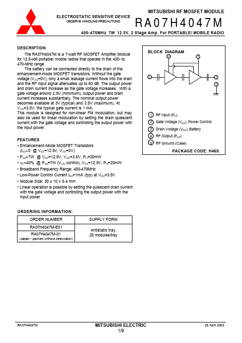
MITSUBISHI RF MOSFET MODULERA30H4047M400-470MHz 30W 12.5V MOBILE RADIOELECTROSTATIC SENSITIVE DEVICEOBSERVE HANDLING PRECAUTIONSDESCRIPTIONThe RA30H4047M is a 30-watt RF MOSFET Amplifier Module for 12.5-volt mobile radios that operate in the 400- to 470-MHz range.The battery can be connected directly to the drain of the enhancement-mode MOSFET transistors. Without the gate voltage (V GG =0V), only a small leakage current flows into the drain and the RF input signal attenuates up to 60 dB. The output power and drain current increase as the gate voltage increases. With a gate voltage around 4V (minimum), output power and drain current increases substantially. The nominal output power becomes available at 4.5V (typical) and 5V (maximum). At V GG =5V, the typical gate current is 1 mA.This module is designed for non-linear FM modulation, but may also be used for linear modulation by setting the drain quiescent current with the gate voltage and controlling the output power with the input power.FEATURES• Enhancemen- Mode MOSFET Transistors (I DD ≅0 @ V DD =12.5V, V GG =0V)• P out >30W, ηT >40% @ V DD =12.5V, V GG =5V, P in =50mW • Broadband Frequency Range: 400-470MHz• Low-Power Control Current I GG =1mA (typ) at V GG =5V • Module Size: 66 x 21 x 9.88 mm• Linear operation is possible by setting the quiescent drain current with the gate voltage and controlling the output power with the input powerORDERING INFORMATION:ORDER NUMBER SUPPLY FORM RA30H4047M-E01RA30H4047M-01(Japan - packed without desiccator)Antistatic tray, 10 modules/tray1 RF Input (Pin )2 Gate Voltage (VGG ), Power Control3 Drain Voltage (V DD ), Battery4 RF Output (P out )5 RF Ground (Case)SALES CONTACTJAPAN:Mitsubishi Electric Corporation Semiconductor Sales Promotion Department 2-2-3 Marunouchi, Chiyoda-kuTokyo, Japan 100Email: sod.sophp@hq.melco.co.jp Phone: +81-3-3218-4854Fax: +81-3-3218-4861GERMANY:Mitsubishi Electric Europe B.V. SemiconductorGothaer Strasse 8D-40880 Ratingen, Germany Email: @ Phone: +49-2102-486-0Fax: +49-2102-486-3670HONG KONG:Mitsubishi Electric Hong Kong Ltd. Semiconductor Division41/F. Manulife Tower, 169 Electric Road North Point, Hong KongEmail: scdinfo@ Phone: +852 2510-0555Fax: +852 2510-9822 FRANCE:Mitsubishi Electric Europe B.V. Semiconductor25 Boulevard des BouvetsF-92741 Nanterre Cedex, France Email: @ Phone: +33-1-55685-668Fax: +33-1-55685-739SINGAPORE:Mitsubishi Electric Asia PTE Ltd Semiconductor Division307 Alexandra Road#3-01/02 Mitsubishi Electric Building, Singapore 159943Email: semicon@ Phone: +65 64 732 308Fax: +65 64 738 984 ITALY:Mitsubishi Electric Europe B.V. SemiconductorCentro Direzionale Colleoni, Palazzo Perseo 2, Via ParacelsoI-20041 Agrate Brianza, Milano, Italy Email: @ Phone: +39-039-6053-10Fax: +39-039-6053-212TAIWAN:Mitsubishi Electric Taiwan Company, Ltd., Semiconductor Department9F, No. 88, Sec. 6Chung Shan N. RoadTaipei, Taiwan, R.O.C.Email: metwnssi@ Phone: +886-2-2836-5288Fax: +886-2-2833-9793 U.K.:Mitsubishi Electric Europe B.V. SemiconductorTravellers Lane, Hatfield Hertfordshire, AL10 8XB, England Email: @ Phone: +44-1707-278-900Fax: +44-1707-278-837U.S.A.:Mitsubishi Electric & Electronics USA, Inc. Electronic Device Group1050 East Arques AvenueSunnyvale, CA 94085Email: customerservice@ Phone: 408-730-5900Fax: 408-737-1129CANADA:Mitsubishi Electric Sales Canada, Inc. 4299 14th AvenueMarkham, Ontario, Canada L3R OJ2 Phone: 905-475-7728Fax: 905-475-1918AUSTRALIA:Mitsubishi Electric Australia, Semiconductor Division348 Victoria Road Rydalmere, NSW 2116 Sydney, AustraliaEmail: semis@ Phone: +61 2 9684-7210+61 2 9684 7212+61 2 9684 7214+61 3 9262 9898 Fax: +61 2 9684-7208+61 2 9684 7245元器件交易网。
X4043中文资料

Applying power to the device activates the power on reset circuit which holds RESET/RESET active for a period of time. This allows the power supply and oscillator to stabilize before the processor can execute code.
The device’s low VCC detection circuitry protects the user’s system from low voltage conditions, resetting the system when VCC falls below the minimum VCC trip point. RESET/RESET is asserted until VCC returns to proper operating level and stabilizes. Five industry standard VTRIP thresholds are available, however, Xicor’s unique circuits allow the threshold to be reprogrammed to meet custom requirements or to fine-tune the threshold for applications requiring higher precision.
RA07H4047M资料
SUPPLY FORM Antistatic tray, 25 modules/tray
RA07H4047M
MITSUBISHI ELECTRIC 1/9
25 April 2003
元器件交易网
ELECTROSTATIC SENSITIVE DEVICE
SYMBOL VDD VGG Pin Pout Tcase(OP) Tstg PARAMETER Drain Voltage Gate Voltage Input Power Output Power Operation Case Temperature Range Storage Temperature Range CONDITIONS VGG<3.5V VDD<12.5V, Pin=0mW f=400-470MHz, ZG=ZL=50Ω
ELECTROSTATIC SENSITIVE DEVICE
OBSERVE HANDLING PRECAUTIONS
MITSUBISHI RF POWER MODULE
RA07H4047M
rd
TYPICAL PERFORMANCE (Tcase=+25°C, ZG=ZL=50Ω, unless otherwise specified)
元器件交易网
MITSUBISHI RF MOSFET MODULE
ELECTROSTATIC SENSITIVE DEVICE
OBSERVE HANDLING PRECAUTIONS
RA07H4047M
BLOCK DIAGRAM
2 3
400-470MHz 7W 12.5V, 2 Stage Amp. For PORTABLE/ MOBILE RADIO
TP3404资料

TL H 11924TP3404Quad Digital Adapter for Subscriber Loops (QDASL)PRELIMINARYJuly 1994TP3404Quad Digital Adapter for Subscriber Loops (QDASL)General DescriptionThe TP3404is a combination 4-line transceiver for voice and data transmission on twisted pair subscriber loops typi-cally in PBX line card applications It is a companion device to the TP3401 2 3DASL single-channel transceivers In addition to 4independent transceivers a time-slot assign-ment circuit is included to support interfacing to the system backplaneEach QDASL line operates as an ISDN ‘‘U’’Interface for short loop applications typically in a PBX environment pro-viding transmission for 2B channels and 1D channel Full-duplex transmission at 144kb s is achieved on single twisted wire pairs using a burst-mode technique (Time Com-pression Multiplexed) All timing sequences necessary for loop activation and de-activation are generated on-chip Alternate Mark Inversion (AMI)line coding is used to ensure low error rates in the presence of noise with lower emi radia-tion than other codes such as Biphase (Manchester) On 24AWG cable the range is at least 1 8km (6k ft)Features4COMPLETE ISDN PBX 2-WIRE DATA TRANSCEIVERS INCLUDINGY Quad 2B plus D channel interface for PBX ‘‘U’’interfaceY 144kb s full-duplex on 1twisted pair using Burst Mode Transmission TechniqueY Loop range up to 6kft ( 24AWG)Y Alternate Mark Inversion coding with transmit Pulse Shaping DAC Smoothing Filter and scrambler for low emi radiationY Adaptive line equalizerY On-chip timing recovery no external componentsY Programmable Time-Slot Assignment TDM interface for B channelsY Separate interface for D channel with Programmable Sub-Slot Assignment Y 4 096MHz master clock Y 4loop-back test modesY MICROWIRE TM compatible serial control interface Y 5V operationY 28-pin PLCC packageBlock DiagramTL H 11924–1TRI-STATE is a registered trademark of National Semiconductor Corporation MICROWIRE TM is a trademark of National Semiconductor Corporation C 1995National Semiconductor CorporationRRD-B30M115 Printed in U S AAbsolute Maximum RatingsIf Military Aerospace specified devices are required please contact the National Semiconductor Sales Office Distributors for availability and specifications V DDA V DDD to GNDA GNDD7V Voltage at Any Li Lo Pin V CC a1V to GND b1V Current at Any Lo g100mA Voltage at Any Digital Input V CC a1V to GND b1V Current at Any Digital Output g50mA Storage Temperature Range b65 C to a150 C Lead Temperature(Soldering 10sec )300 CElectrical Characteristics Unless otherwise specified limits printed in BOLD characters are guaranteed for V CCA e V CCD e5V g5% T A e0 C to a70 C Typical characteristics are specified at V DDA e V DDD e5 0V T A e25 C All signals are referenced to GND which is the common of GNDA and GNDDSymbol Parameter Conditions Min Typ Max Units DIGITAL INTERFACESV IH Input High Voltage All Digital Inputs(DC)2V V IL Input Low Voltage All Digital Inputs(DC)0 8V V OH Output High Voltage I L e a1mA2 4V V OL Output Low Voltage I L e b1mA0 4V I IL Input Low Current All Digital Input GND k V IN k V IL b1010m A I IH Input High Current All Digital Input V IH k V IN k V CC b1010m AI OZ Output Current in High Impedance BO CO and DOb1010m A (TRl-STATE )LINE INTERFACESR Li Input Resistance0V k V Li k V CC20k X C LLo Load Capacitance From Lo to GND200pF ROLS Output Resistance Load e60X in Series with2m F to GND3XV DC Mean DC Voltage at Lo Load e200X in Series with2m F to GND1 752 25VVoltage at LS a LS bPOWER DISSIPATIONI CC0Power Down Current BCLK e0Hz MCLK e0Hz CCLK e0Hz10mA I CC1Power Up Current All4Channels Activated75mA TRANSMISSION PERFORMANCETransmit Pulse Amplitude at Lo R L e200X in Series with2m F to GND1 11 31 5VpkInput Pulse Amplitude at Li g60mVpk TIMING SPECIFICATIONSSymbol Parameter Conditions Min Typ Max Units MASTER CLOCK INPUT SPECIFICATIONSf MCLK Frequency of MCLK4 096MHzMaster Clock Tolerance Relative2X MCLK in Slave b100a100ppm t WMH Period of MCLK High Measured from V IH to V IH70ns t WML Period of MCLK Low Measured from V IL to V IL70ns t RM Rise Time of MCLK Measured from V IL to V IH15ns t FM Fall Time of MCLK Measured from V IH to V IL15ns2Electrical Characteristics Unless otherwise specified limits printed in BOLD characters are guaranteed for V CCA e V CCD e5V g5% T A e0 C to a70 C Typical characteristics are specified at V DDA e V DDD e5 0V T A e25 C All signals are referenced to GND which is the common of GNDA and GNDD(Continued)TIMING SPECIFICATIONS(Continued)Symbol Parameter Conditions Min Typ Max UnitsDIGITAL INTERFACE TIMINGf BCLK BCLK Frequency4 0964 1MHzt WBH Clock Pulse Width High Measured from V IH to V IH70ns t WBL and Low for BCLK Measured from V IL to V IL70t RB Rise Time and Fall Time Measured from V IL to V IH15ns t FB of BCLK Measured from V IH to V IL15t HBM BCLK Transition to MCLK High or Low b3030nst SFC Set up Time FS Valid to BCLK Invalid204nst HCF Hold Time BCLK Low to FS Invalid4030nst SBC Setup Time BI Valid to BCLK Invalid3011nst HCB Hold Time BCLK Valid to BI Invalid407nst SDC Setup Time DI Valid to BCLK Low30nst HCD Hold Time BCLK Low to DI Invalid40nst DCB Delay Time BCLK High to BO Valid Load e2LSTTL a100pF80nst DCBZ Delay Time BCLK Low to BO High-Z80120nst DCD Delay Time BCLK High to DO valid Load e2LSTTL a100pF80nst DCZ Delay Time BCLK Low to DO High40120ns Impedancet DCT Delay Time BCLK High to TSB Low120nst ZBT Disable Time BCLK Low to TSB High-Z120nsMICROWIRE CONTROL INTERFACE TIMINGf CCLK Frequency of CCLK2 1MHzt CH Period of CCLK High Measured from V IH to V IH150nst CL Period of CCLK Low Measured from V IL to V IL150nst SSC Setup Time CS Low to CCLK High50nst HCS Hold Time CCLK High to CS Transition40nst SIC Setup Time CI Valid to CCLK High50nst HCI Hold Time CCLK High to CI Invalid20nst DCO Delay Time CCLK Low to CO Valid80nst DSOZ Delay Time CS High to CO High-Z80nst DCIZ Delay Time CCLK to INT High-Z100ns Notes For the purposes of this specification the following conditions applya All input signals are defined as V IL e0 4V V IH e2 7V t r k10ns t f k10nsb Delay times are measured from the input signal Valid to the output signal Validc Setup times are measured from the Data input Valid to the clock input Invalidd Hold times are measured from the clock signal Valid to the Data input Invalid3Pin DescriptionsPin PinDescriptionNo Name1GNDA Analog Ground or0V All analog signals are referenced to this pin15GNDD Digital Ground0V It must connect to GNDA with a shortest possible trace This can be done directly underneath the part28VDDA Positive power supply input to QDASL analog section It must be5V g5%16VDDD Positive power supply input to QDASL digital section It must be5V g5% and connect to VDDA with the shortest possible trace This can be done directly underneath the part11FS Frame Sync input this signal is the8kHz clock which defines the start of the transmit and receive frames at the digital interfaces9MCLK This pin is the4 096MHz Master Clock input which requires a CMOS logic level clock from a stable source MCLK must be synchronous with BCLK10BCLK Bit Clock logic input which determines the data shift rate for B and D channel data at the BI BO DI and DO pins BCLK may be any multiple of8kHz from256kHz to4 096MHz but must be synchronous with MCLK12BI Time-division multiplexed input for B1and B2channel data to be transmitted to the4lines Data on this pin is shifted in on the failing edge of BCLK into the B1and B2channels during the selected transmit time-slots13BO Time-division multiplexed receive data output bus B1and B2channel data from all4lines is shifted out on the rising edge of BCLK on this pin during the assigned receive time-slots At all other times this output isTRI-STATE(high impedance)14TSB This pin is an open-drain output which is normally high impedance but pulls low during any active B channel receive time slots at the BO pin7DI Time-division multiplexed input for D channel data to be transmitted to the4lines Data on this pin is shifted in on the failing edge of BCLK into the D channel during the selected transmit sub-time-slots8DO Time-division multiplexed output for D channel data received from the4lines Data on this pin is shifted out on the rising edge of BCLK during the selected receive sub-time-slot19CCLK Microwire Control Clock input This clock shifts serial control information into CI and out from CO when the CS input is low depending on the current instruction CCLK may be asynchronous with the other system clocks21CI Control data Input Serial control information is shifted into the QDASL on this pin on the rising edges of CCLK when CS is low17INT Interrupt request output a latched output signal which is normally high impedance and goes low to indicate a change of status of any of the4loop transmission systems This latch is cleared when the Status Register isread by the microprocessor Bipolar Violation does not effect this output20CO Control data Output Serial control status information is shifted out from the QDASL on this pin on the falling edges of CCLK when CS is low18CS Chip Select input When this pin is pulled low the Microwire interface is enabled to allow control information to be written in to and out from the device via the CI and CO ins When high this pin inhibits the Microwireinterface4Lo0Line driver transmit outputs for the4transmission channels Each output is an amplifier intended to drive a transformer3Lo126Lo225Lo35Li0Line receive amplifier inputs for the4transmission channels Each Li pin is a self-biased high impedance input which should be connected to the transformer via the recommended line interface circuit2Li127Li224Li34Connection DiagramTL H 11924–2Top ViewOrder Number TP3404V See NS Package Number V28AFunctional DescriptionThe QDASL contains 4transceivers each of which can in-teroperate with any of the TP340X family of single-channel DASL transceivers Each QDASL transceiver has its own independent line transmit and receive section timing recov-ery circuit scrambler descrambler and loop activation con-troller Functions which are shared by the 4transceivers include the Microwire control port and the digital interface with time-slot assignmentBURST MODE OPERATIONFor full-duplex operation over a single twisted-pair burst mode timing is used with the QDASL end of each line act-ing as the loop timing master and the DASL at the terminal being the timing slave (the QDASL transceivers cannot op-erate in loop timing slave mode)Each burst within a DASL line is initiated by the QDASL Master transmitting a startbit for burst framing followed by the B1 B2and D channel data from 2consecutive 8kHz frames combined in the format shown in Figure 1 During transmit bursts the receiver input for that channel is inhibit-ed to avoid disturbing the adaptive circuits The slave’s re-ceiver is enabled at this time and it synchronizes to the start bit of the burst which is always an unscrambled ‘‘1’’(of the opposite polarity to the last ‘‘1’’sent in the previous burst) When the slave detects that 36bits following the start bit have been received it disables the received input waits 6line symbol periods to match the other end settling guard time and then begins to transmit its burst back towards the master which by this time has enabled its receiver input The burst repetition rate is thus 4KHzLINE TRANSMIT SECTIONSAlternate Mark Inversion (AMI)line coding in which binary ‘‘1’’s are alternately transmitted as a positive pulse then a negative pulse is used on each DASL line because of its spectral efficiency and null DC energy content All transmit-ted bits excluding the start bit are scrambled by a 9-bit scrambler to provide good spectral spreading with a strong timing content The scrambler feedback polynomial is X 9a X 5a 1TL H 11924–3FIGURE 1 Burst Mode Timing on the Line5Functional Description (Continued)Pulse shaping is obtained by means of a Digital to Analog Converter followed by a Continuous Smoothing Filter in or-der to limit RF energy and crosstalk while minimizing Inter-Symbol Interference (ISI) Figure 2shows the pulse shape at the Lo output while a template for the typical power spectrum transmitted to the line with random data is shown in Figure 3Each line-driver output Lo0–Lo3 is designed to drive a transformer through a capacitor and termination resistor A 1 1transformer terminated in 100X results in signal ampli-tude of typically 1 3Vpk on the line Over-voltage protection must be included in each interface circuitLINE RECEIVE SECTIONSThe input of each receive section Li0–Li3 consists of a continuous anti-alias filter followed by a switched-capacitor low-pass filter designed to limit the noise bandwidth withminimum intersymbol interference To correct pulse attenu-ation and distortion caused by the transmission line an AGC circuit and first-order equalizer adapt to the received pulse shape thus restoring a ‘‘flat’’channel response with maxi-mum received eye opening over a wide spread of cable attenuation characteristicsFrom the equalized output a DPLL (Digital Phase-Locked Loop)recovers a low-jitter clock for optimum sampling of the received symbols The MCLK input provides the refer-ence clock for the DPLL at 4 096MHzFollowing detection of the recovered symbols the received data is de-scrambled by the same X 9a X 5a 1polynomial and presented to the digital system interface circuitWhen a transmission line is de-activated a Line-Signal De-tect Circuit is enabled to detect the presence of incoming bursts if the far-end starts to activate the loopTL H 11924–4FIGURE 2 Typical AMI Waveform at LoTL H 11924–5FIGURE 3 Typical AMI Transmit Spectrum Measured at LO Output (With RGB e 100Hz)6Functional Description(Continued)ACTIVATION AND LOOP SYNCHRONIZATION Activation(i e power-up and loop synchronization)may be initiated from either end of the loop If the master(QDASL) end is activating the loop it sends normal bursts of scram-bled‘‘1’’s which are detected by the slave’s line-signal-de-tect circuitry The slave then replies with bursts of scram-bled‘‘1’’s synchronized to the received bursts and the Framing Detection circuit at each end searches for4con-secutive correctly formatted receive bursts to acquire full loop synchronization The QDASL receiver indicates when it is correctly in sync with received bursts by setting an indica-tion in the Status Register and pulling the INT pin lowFor the slave end to initiate activation it begins transmission of alternate bursts i e the burst repetition rate is2KHz not 4KHz At this point the slave is running from its local oscilla-tor and is not receiving any sync information from the mas-ter When the master’s Line-Signal Detect Circuit recogniz-es this‘‘wake-up’’signal the appropriate QDASL line must be activated by writing to the Control Register The master begins to transmit bursts synchronized as normal to the FS input with a4KHz repetition rate This enables the slave’s receiver to correctly identify burst timing from the master and to re-synchronize its own burst transmissions to those it receives The Framing Detection Circuits then acquire full loop sync as described earlierLoop synchronization is considered to be lost if the Framing Detection Circuit does not find four framing marks of the four consecutive4KHz line frames At this point an indica-tion is set in the Status Register the INT output is pulled low and the receiver searches to re-acquire loop sync MICROWIRE CONTROL INTERFACEA serial interface which can be clocked independently from theB and D channel system interfaces is provided for mi-crocontroller access to the time-slot assignment Control and Status Registers in the QDASL The microcontroller is normally the timing master of this interface and it supplies the CCLK and CS signals All data transfers consist of simultaneous read and write cycles in which2continuous bytes are sampled on the CI pin at the same time as2bytes are shifted out from the CO pin see Figure6 The first byte is a register address and the second is the data To initiate a Microwire read write cycle CS must be pulled low for16cycles of CCLK Data on CI is sampled on rising edges of CCLK and shifted out from CO on failing edges When CS is high the CO pin is in the high-impedance TRI-STATE enabling the CO pins of many de-vices to be multiplexed togetherWhenever a change(except Bipolar Violation)in any of the QDASL status conditions occurs the Interrupt output INT is pulled low to alert the microprocessor to initiate a read cycle of the Status Register This latched output is cleared when the read cycle is initiatedTable1lists the address map of control functions and status indicators Table2lists the addresses for the Control Registers for each QDASL line Even-numbered addresses are read-write cycles in which the data returned by the CO pin is previous contents of the addressed register Odd-numbered addresses are readback commands onlyTABLE I Global Register Address Map AddressRegisters(Hex)00–0F LINE0Control(TSX TSR CTRL)10–1F LINE1Control(TSX TSR CTRL)20–2F LINE2Control(TSX TSR CTRL)30–3F LINE3Control(TSX TSR CTRL)40–CF Not usedFF Common Status Register for all lines(0–3)See Table VITABLE II Per Line Control Register Address MapFunctionByte1(Note2)Byte2 MSB NibbleLSB Nibble(Note1)76543210Write TSXD Register N0000See Table V Read TSXD Register N0001See Table V Write TSXB1Register N0010See Table IV Read TSXB1Register N0011See Table IV Write TSXB2Register N0100See Table IV Read TSXB2Register N0101See Table IV Write TSRD Register N0110See Table V Read TSRD Register N0111See Table V Write TSRB1Register N1000See Table IV Read TSRB1Register N1001See Table IV Write TSRB2Register N1010See Table IV Read TSRB2Register N1011See Table IV Write Line Control Register(CTR L)N1110See Table III Read Line Control Register(CTRL)N1111See Table IIINote1 N e0 1 2 or3in straight Binary notation for Line0 1 2 or3respectivelyNote2 Bit7of bytes1and2is always the first bit clocked into or out from the CI and CO pins7Functional Description(Continued)LINE CONTROL REGISTERS CTRLNEach of the4transceivers has a Line Control Register CTRL0–CTRL3 which provides for control of loop activa-tion Ioopbacks Interrupt enabling and D channel interface enabling Table3lists the functionsPOWER ON INITIALIZATIONFollowing the initial application of power the QDASL enters the power-down(de-activated)state in which all the internal circuits are inactive and in a low power state except for a Line-Signal Detect Circuit for each of the4lines and the necessary bias circuits The4line outputs Lo0–Lo3 are in a high impedance state and all digital outputs are inactive All bits in the Line Control Registers power-up initially set to ‘‘0’’ While powered-down each Line-Signal Detect Circuit continually monitors its line to detect if the far-end initiates loop transmissionPOWER-UP DOWN CONTROLTo power-up the device and initiate activation bit C7in any of the4Line Control Registers must be set high see Table III Setting C7low de-activates the loop or puts the channel in power-down state During power-down state internal reg-ister data is retained and still can be accessed LOOPBACKSFour different loopbacks can be set for each line They are enabled and disabled by setting the corresponding bits in the Control Register see Table III In addition a line must be activated to see the effect of loopback commands1 2B a D Line LoopbackWhen bit5is set to1 this loop will transfer all three channels B1 B2and D that are received at the Li pin back to the Lo pin Data out on BO DO is still the same as received at the Li input 2 B1Line LoopbackWhen bit4is set high the loop path is the same as(1) but only data on the B1channel is looped back to the line Transmit data in the B2and D channels is from the Bi DI pins3 B2Line LoopbackAs(2)but for the B2channel4 2B a D Digital LoopbackThis loop will transfer all data(2B a D)received at BI DI back to BO DO The data is also transmitted to the line TIME-SLOT ASSIGNMENTThe digital interface of the QDASL uses time-division multi-plexing with data framed in up to64possible8-bit time-slots per125m s frame Channels B1and B2for all4lines are clocked in(towards the line)at the BI pin and clocked out(from the line)at the BO pin A separate port is provided for the D channel data for all4lines which is clocked in on DI and out on DO In addition to time-slot assignment D channel data may be assigned into2-bit sub-slots within each time slot with up to256sub-slots per frame(with BCLK e4 096MHz) Each frame starts with the first posi-tive edge of BCLK after the FS signal goes high and count-ing of timeslots starts from zero at the beginning of the frame Figure4shows the timing with some example time-slot assignmentsFor each of the4QDASL lines there are6Time-Slot As-signment control registers one each for transmit and re-ceive B1 B2and D channels Selection of time-slots for transmit data into the BI or DI pin is made by writing the timeslot number(in Hex notation)into the appropriate TSX register TSXB1is the time-slot assignment for the transmit B1 TSXB2is the time-slot assignment register for the trans-mit B2channel and TSXD is the sub-slot assignment regis-ter for the transmit D channelTABLE III Byte2of Control Register(CTRLN)Bit NumberFunction765432100Deactivate Line1Activate Line0Disable Digital Loopback1Enable2B a D Digital Loopback 0Disable Line Loopback1Enable2B a D Line Loopback0Disable B1Line Loopback1Enable B1Line Loopback0Disable B2Line Loopback1Enable B2Line Loopback0Disable Interrupt from this Line1Enable Interrupt from this Line0D Channel enabled from DO to Line1D Channel disabled from DO to Line0D Channel enabled from Line to DI1D Channel disabled from Line to DI8Functional Description(Continued)In the same manner the time-slot number should be written into the appropriate TSR registers for receive data at the BO and DO pins TSRB1is the time-slot assignment for the receive B1channel TSRB2is the time-slot assignment reg-ister for the receive B2channel and TSRD is the sub-slot assignment register for the receive D channelWhenever any receive time-slot is active at BO the TSB output is also pulled lowREGISTERS TSXB1 TSXB2 TSRB1 TSRB2The data format for all B channel time-slot assignment reg-isters is shown in Table IVBit7Transparency Control EBThis bit enables or disables data transparency between the digital interface and the line interface for the selected chan-nelEB e0disables the channelEB e1enables the channelWhen the transmit direction(towards the line)is disabled there will be all‘‘ONE’s’’(scrambled)as data for this chan-nel at the Lo pin If the receive direction(from the line)is disabled BO will stay high impedance for the programmed time slot while if it is enabled data out on BO in the as-signed time slot is the data from LiBits5–0 TS5–TS0These bits define the binary number of the time-slot select-ed Time-slots are numbered from0–63 The frame sync signal is used as marker pulses for the beginning of time slot0TABLE IV Byte2of Register TSXB1 TSXB2 TSRB1or TSRB2for B Channel Time-Slot AssignmentBit Number and NameFunction 76543210EB X TS5TS4TS3TS2TS1TS00X X X X X X X Disable B1and or B2 1X Assign One Binary Coded Time-Slot Enable B1and or from0–63B2Note If two B channels are erroneously assigned to the same time-slot data out on Bo is not valid while data out on Lo is valid REGISTERS TXD TRDThe data format for all D channel time-slot assignment reg-isters is as followsData transparency between the digital interface and the line interface for the D channels can be controlled via the Chan-nel Control Register see Table IIIBits7–0 TS7–TS0These bits define the binary number of the sub-slot select-ed Sub-slots are numbered from0–255 The frame sync signal is used as marker pulses for the beginning of Sub-slot 0TABLE V Byte2of Register TSXD or TSRD for DChannel Time-Slot AssignmentBit Number and Name76543210SS SS SS SS SS SS SS SS76543210 Assign One Binary Coded Sub-Slot from0–255for D ChannelTL H 11924–6FIGURE4 QDASL Digital Interface Timing9Functional Description(Continued)TABLE VI Status Register FunctionsByte2Indication7654321000Line3 deactivated01Line3 line signal present but not in sync10Line3 activated bipolar violation(Note1)11Line3 activated no bipolar violation00Line2 deactivated01Line2 line signal present but not in sync10Line2 activated bipolar violation(Note1)11Line2 activated no bipolar violation00Line1 deactivated01Line1 line signal present but not in sync10Line1 activated bipolar violation(Note1)11Line1 activated no bipolar violation00Line0 deactivated01Line0 line signal present but not in sync10Line0 activated bipolar violation(Note1)11Line0 activated no bipolar violation Note1 Bipolar Violation does not cause an InterruptSTATUS REGISTERStatus information for all4channels may be read from the common Status Register by addressing location X FF 2bits per line are coded as shown in Table VI A change in the status of1or more lines is indicated by the INT pin being pulled low provided bit2of the corresponding control regis-ter is set to‘‘ONE’’to enable the interrupt for that line BIPOLAR VIOLATION DETECTOROn an activated line whenever a line error is received there will be a violation of the AMI coding rule This is reported by setting the code10for that line The violation indication is cleared to11after a read of the Status RegisterAs an example of the interpretation of the Status Register contents if the byte2read back from the Status Register e00111001(e X 39) this indicates the following status of the4lines line3is deactivated line2is in sync with no error since the last read cycle line1is in sync but there has been1or more errors since the last read cycle of the Status Register line0is receiving a line signal but the line trans-mission is not synchronizedApplications InformationPOWER SUPPLIESWhile the pins of the TP3404QDASL device are well pro-tected against electrical misuse it is recommended that the standard CMOS practice of applying GND to the device be-fore any other connections are made should always be fol-lowed In applications where the printed circuit card may be plugged into a hot socket with power and clocks already present an extra long ground pin on the connector should be usedTo minimize noise sources the VDDA and VDDD pins should be connected together via the shortest possible trace likewise the GNDA and GNDD pins must be connect-ed together These two connections can be done directly underneath the part All other ground connections to each device should meet at a common point as close as possible to the GNDD pin in order to prevent the interaction of ground return currents flowing through a common bus im-pedance A power supply decoupling capacitor of0 1m F should be connected from this common point to VDDD as close as possible to the device pinsFigure5shows a typical4line application of the QDASL The current list of suitable commercial transformers isSchott Corporation(Nashville)Phone615-889-8800Part numbers 67110850(dry)67110860(50mA DC)Pulse Engineering(San Diego)Phone619-674-8100Part number TBDNote that the zener diode protection shown in Figure8is only intended as secondary protection for inside wiring ap-plications primary protection is also necessary Further in-formation can be found in the datasheet for the TP3401 2 3DASL devices and in Application Note AN-509‘‘Using the TP3401 2 3ISDN PBX Transceivers’’10。
- 1、下载文档前请自行甄别文档内容的完整性,平台不提供额外的编辑、内容补充、找答案等附加服务。
- 2、"仅部分预览"的文档,不可在线预览部分如存在完整性等问题,可反馈申请退款(可完整预览的文档不适用该条件!)。
- 3、如文档侵犯您的权益,请联系客服反馈,我们会尽快为您处理(人工客服工作时间:9:00-18:30)。
LM40411.225V Precision micropower shunt voltage referenceDescriptionOrdering informationThe LM4041 is a bandgap circuit designed to achieve a precision micro-power voltage reference of 1.225 V. The device is available in the small outline SOT23 surface mount packages which is ideal for applications where space saving is important.The LM4041 is available to 0.5% C grade for precision applications. Excellent performance is maintained over the 60A to 12mA operating current range with a typical temperature coefficient of only 20ppm/°C.The device has been designed to be highly tolerant of capacitive loads so maintaining excellent stability.This device offers a pin for pin compatible alternative to the LM4041 voltage reference.Features•Small packages: SOT23•No output capacitor required •Output voltage tolerance •LM4041C ±0.5% at 25°C •LM4041D±1% at 25°C•Low output noise(10 Hz to 10kHz) ........... 60Vrms•Wide operating current range 60A to 12mA •Extended temperature range -40°C to +125°C •Low temperature coefficient 100ppm/°C (max)Applications•Battery powered equipment •Precision power supplies •Portable instrumentation•Portable communications devices •Notebook and palmtop computers •Data acquisition systemsPinout information25°C tol.Voltage (V)Order code Pack Part markStatus Reel size Tape width QuantIty per reel 0.5% 1.225LM4041CFTA SOT23R1C Preview 7”, 180mm 8mm 30001%1.225LM4041DFTASOT23R1D Preview7”, 180mm8mm3000Absolute maximum ratingsContinuous reverse current (I KA).................................... 20mAContinuous forward current (I REF).................................. 10mAOperating junction temperature..................................... -40°C to 150°CStorage temperature ....................................................... -55°C to 150°COperation above the absolute maximum rating may cause device failure. Operation at the absolute maximum ratings, for extended periods, may reduce device reliability.Unless otherwise stated voltages specified are relative to the ANODE pin.Package thermal dataPackage⍜JA P DIST amb =25°C, T J = 150°CSOT23380°C/W330mWRecommended operating conditionsMin.Max.UnitsReverse current0.0615mAOperating ambient temperature range-40125°CElectrical characteristicsOver recommended operating conditions, T amb = 25°C, unless otherwise stated. LM4041C and LM4041D have initial tolerances of 0.5% and 1% respectively.Symbol Parameter Conditions Typ.LM4041CLimits LM4041DLimitsUnitsT ambV REF Reverse breakdownvoltageI R = 100 A25°C 1.225VReverse breakdownvoltage toleranceI R = 100A25°C±6±12mV-40 to 85°C±14±24-40 to 125°C±18.4±31I RMIN Minimum operatingcurrent25°C456065µA -40 to 85°C6570-40 to 125°C6873⌬V R/⌬T Average reversebreakdown voltagetemperature coefficientI R = 10 mA-40 to 125°C±20ppm/°CI R = 1 mA,±15±100±150I R = 100 A±15⌬V R/⌬I R Reverse breakdownchange with current I RMIN < I R <1mA25°C0.71.52.0mV -40 to 85°C 2.0 2.5-40 to 125°C 2.0 2.51mA < I R <12 mA25°C2.56.08.0-40 to 85°C8.010.0-40 to 125°C8.010.0Z R Dynamic outputimpedance I R = 1mA, f = 120HzI AC = 0.1I R0.5 1.5 2.0⍀e n Noise voltage I R = 100A10Hz < f < 10kHz60V RMS⌬V R Long term stability (non cumulative)t = 1000HrsI R = 100A120ppmPackage outline - SOT23Note: Controlling dimensions are in millimeters. Approximate dimensions are provided in incheslimeters Inches limeters Inches Min.Max.Min.Max.Min.Max.Max.Max.A - 1.12-0.044e1 1.90 NOM0.075 NOMA10.010.100.00040.004E 2.10 2.640.0830.104b 0.300.500.0120.020E1 1.20 1.400.0470.055C 0.0850.1200.0030.008L 0.250.620.0180.024D 2.803.040.1100.120L10.450.620.0180.024e0.95NOM 0.0375NOM-----Intentionally left blankZetex sales offices EuropeZetex GmbHKustermann-park Balanstraße 59D-81541 München GermanyTelefon: (49) 89 45 49 49 0Fax: (49) 89 45 49 49 49europe.sales@AmericasZetex Inc700 Veterans Memorial Highway Hauppauge, NY 11788USATelephone: (1) 631 360 2222Fax: (1) 631 360 8222usa.sales@Asia PacificZetex (Asia Ltd)3701-04 Metroplaza Tower 1Hing Fong Road, Kwai Fong Hong KongTelephone: (852) 26100 611Fax: (852) 24250 494asia.sales@Corporate HeadquartersZetex Semiconductors plcZetex Technology Park, Chadderton Oldham, OL9 9LL United KingdomTelephone: (44) 161 622 4444Fax: (44) 161 622 4446hq@© 2006 Published by Zetex Semiconductors plcDefinitionsProduct changeZetex Semiconductors reserves the right to alter, without notice, specifications, design, price or conditions of supply of any product or service. Customers are solely responsible for obtaining the latest relevant information before placing orders.Applications disclaimerThe circuits in this design/application note are offered as design ideas. It is the responsibility of the user to ensure that the circuit is fit for the user’s application and meets with the user’s requirements. No representation or warranty is given and no liability whatsoever is assumed by Zetex with respect to the accuracy or use of such information, or infringement of patents or other intellectual property rights arising from such use or otherwise. Zetex does not assume any legal responsibility or will not be held legally liable (whether in contract,tort (including negligence), breach of statutory duty, restriction or otherwise) for any damages, loss of profit, business, contract,opportunity or consequential loss in the use of these circuit applications, under any circumstances.Life supportZetex products are specifically not authorized for use as critical components in life support devices or systems without the express written approval of the Chief Executive Officer of Zetex Semiconductors plc. As used herein:A. Life support devices or systems are devices or systems which:1.are intended to implant into the body or2.support or sustain life and whose failure to perform when properly used in accordance with instructions for use provided in the labelling can be reasonably expected to result in significant injury to the user.B. A critical component is any component in a life support device or system whose failure to perform can be reasonably expected tocause the failure of the life support device or to affect its safety or effectiveness.ReproductionThe product specifications contained in this publication are issued to provide outline information only which (unless agreed by the company in writing) may not be used, applied or reproduced for any purpose or form part of any order or contract or be regarded as a representation relating to the products or services concerned. Terms and ConditionsAll products are sold subjects to Zetex’ terms and conditions of sale, and this disclaimer (save in the event of a conflict between the two when the terms of the contract shall prevail) according to region, supplied at the time of order acknowledgement.For the latest information on technology, delivery terms and conditions and prices, please contact your nearest Zetex sales office or visit: Quality of productZetex is an ISO 9001 and TS16949 certified semiconductor manufacturer.To ensure quality of service and products we strongly advise the purchase of parts directly from Zetex Semiconductors or one of our regionally authorized distributors. For a complete listing of authorized distributors please visit: /salesnetworkZetex Semiconductors does not warrant or accept any liability whatsoever in respect of any parts purchased through unauthorized sales channels.ESD (Electrostatic discharge)Semiconductor devices are susceptible to damage by ESD. Suitable precautions should be taken when handling and transporting devices.The possible damage to devices depends on the circumstances of the handling and transporting, and the nature of the device. The extent of damage can vary from immediate functional or parametric malfunction to degradation of function or performance in use over time.Devices suspected of being affected should be replaced.Green complianceZetex Semiconductors is committed to environmental excellence in all aspects of its operations which includes meeting or exceeding regulatory requirements with respect to the use of hazardous substances. Numerous successful programs have been implemented to reduce the use of hazardous substances and/or emissions.All Zetex components are compliant with the RoHS directive, and through this it is supporting its customers in their compliance with WEEE and ELV directives.Product status key:“Preview”Future device intended for production at some point. Samples may be available “Active”Product status recommended for new designs “Last time buy (LTB)”Device will be discontinued and last time buy period and delivery is in effect “Not recommended for new designs”Device is still in production to support existing designs and production “Obsolete”Production has been discontinued Datasheet status key:“Draft version”This term denotes a very early datasheet version and contains highly provisional information, whichmay change in any manner without notice.“Provisional version”This term denotes a pre-release datasheet. It provides a clear indication of anticipated performance.However, changes to the test conditions and specifications may occur, at any time and without notice.“Issue”This term denotes an issued datasheet containing finalized specifications. H owever, changes tospecifications may occur, at any time and without notice.。