G9161中文资料
黄金首饰硬度及其强化机制

安环与分析黄 金GOLD2023年第11期/第44卷黄金首饰硬度及其强化机制收稿日期:2023-06-01;修回日期:2023-09-08基金项目:山东计量测试学会科技项目(2021KJ12,2020KJ09)作者简介:李桂华(1982—),女,正高级工程师,博士,从事贵金属材料检测及研究工作;E mail:guihual12@163.com李桂华1,2,丁秀云1,2,刘雪松1,2,臧 军1,程佑法1,2,孙永军3,祝培明2(1.山东省计量科学研究院山东省计量检测重点实验室;2.国家黄金钻石制品质量检验检测中心;3.济南轨道交通集团有限公司)摘要:硬度是反映材料耐磨性的一个重要指标,黄金首饰,尤其是高成色黄金首饰,除传统足金外,还有“3D”硬金、“5G”黄金及“古法”金首饰。
查阅已发表的关于黄金首饰硬度的相关文献,并结合多年积累的黄金首饰维氏硬度数据,总结了常见足金和彩色18K金首饰的硬度,可为评价各类黄金首饰的耐磨性提供数据支撑。
同时,参考金属材料的经典强化机制,结合各类首饰的加工工艺,分析了常见黄金首饰的硬化机制。
关键词:黄金首饰;硬度;强化机制;18K金;足金 中图分类号:TS934 文章编号:1001-1277(2023)11-0100-05文献标志码:Adoi:10.11792/hj20231121引 言随着中国经济的快速发展和生活水平的提高,人们对黄金首饰购买和收藏的需求越来越大,贵金属行业也随之快速发展。
黄金首饰具有优异的物理化学性质,其抗腐蚀能力强、化学性质稳定,但高纯度黄金首饰硬度较低,长期佩戴易发生变形、磨损,严重影响首饰外观[1]。
相同条件(摩擦系数、成分、组织、环境等)下,硬度和耐磨性存在非线性正比关系,通常将硬度作为衡量材料耐磨性的重要指标之一。
材料硬度越高,耐磨性越好[2]。
因此,可通过黄金首饰的硬度来衡量首饰的耐磨性,即首饰硬度越高,耐磨性越好。
硬度的测试方法很多,常用的有布氏硬度、洛氏硬度、维氏硬度等。
火电企业档案分类表
火电企业档案分类表一、修订说明《火电企业档案分类表》由原能源部1991年制定发布执行的。
2002年10月原国家电力公司根据电力工业的发展情况,修订发布了《火电企业档案分类表(6—9大类)》(修订本)。
然而由于电力改制,资产重组,各发电企业的档案工作都出现了不少新情况、新问题,因此我们在结合国华电力公司的实际情况下,根据国家档案局、国务院国有资产监督管理委员会2004年1月颁发的《国有企业文件材料归档办法》的规定,在原能源部《电力工业企业档案分类表(0-5大类)》和国家电力公司《火电企业档案分类表(6-9大类)》(修订本)的框架基础上,保留了经实践证明实用的内容,修改了不适用或已有变化的内容,调整了过时的类目,补充了新的类目与内容,对《火电企业档案分类表》进行了修订。
使档案分类在国华电力公司所属各发电公司能得到规范统一,以便于各单位的档案人员正确掌握与操作运用,同时为档案信息化管理,实现信息共享做准备。
二、关于文件类目交叉问题的规定:1 关于项目合同、协议类文件的归类。
各发电公司在经营、商务、技术服务等活动中签订的合同、协议,归入“290”。
在基建、技改与检修项目活动中签订的合同、协议,归入“8031” 类目。
依次类推技改与检修项目的招、投标文件及评标文件归入“8032”类目。
2 关于设备档案的类目划分。
由设备制造厂家提供的说明书、技术文件、图纸和由厂家负责安装的设备所形成的技术文件、调试记录,以及设备投入运行后检修、技改项目中形成的档案归入“9大类”的相应类目。
由设计院提供的涉及土建施工、系统布置、设备安装的图纸和竣工图归入“8大类”的相应类目。
3 关于钢结构图纸的类目划分。
与设备档案类目划分一样,由设备厂家提供的图纸归入“9大类”的相应类目。
由设计院出的图纸归入“8大类”的相应类目。
4 关于小型基建与技改项目文件的类目划分。
小型基建项目文件,按国华电力公司基建管理程序审批的小型项目,其形成的全部文件材料可组成若干卷,归入“8大类”的相应类目。
RDS82480XXOO中文资料
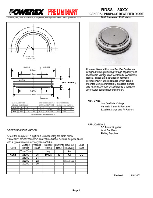
FEATURES:Low On-State VoltageHermetic Ceramic Package Excellent Surge and I 2t RatingsAPPLICATIONS:DC Power Supplies ORDERING INFORMATIONInput Rectifiers Plating SuppliesSelect the complete 12 digit Part Number using the table below.EXAMPLE: RDS82280XXOO is a 2200V-8000A General Purpose DiodeRevised:916/2002Powerex General Purpose Rectifier Diodes are designed with high locking voltage capability and low forward voltage drop to minimize conduction losses. These are packaged in hermetic, ceramic Pow-R-Disc packages which can be mounted using commercially available clamps and heatsinks or fully assembled to a variety of air or water cooled heat exchangers.Absolute Maximum RatingsCharacteristic Symbol Rating UnitsRepetitive Peak Reverse Voltage V RRM2500VoltsNon-repetitive Transient Peak Reverse Voltage V RSM V RRM + 100VoltsAverage On-State Current, T C=90°C I F(Avg.)8000ARMS On-State Current, T C=90°C I F(RMS)12566APeak One Cycle Surge Current, 60Hz, V R=V RRM I FSM100,000AFuse Coordination I2t, 60Hz I2t 4.17E+07A2s Peak One Cycle Surge Current, 50Hz, V R=0V I FSM92,500AFuse Coordination I2t, 50Hz I2t 3.57E+07A2s Operating Temperature Tj-40 to+175°CStorage Temperature T Stg.-50 to+200°CApproximate Weight 6.5lb2.95KgMounting Force16,000 - 20,000lbs71.2 - 89.0KnewtonsElectrical Characteristics, Tj=25°C unless otherwise specifiedRatingCharacteristic Symbol Test Conditions min typ max Units Repetitive Peak ReverseLeakage Current ITj=175°C, V RRM=Rated150300maRRMPeak On-State Voltage V FM Tj=175°C, I FM=4000A0.82VV FM Model, Low Level V0Tj=175°C0.654V VFM = V O +r•I FM r15% I FM- π•I FM 3.82E-05ΩV FM Model, High Level V0Tj=175°C0.786V VFM = V O +r•I FM rπ•I FM - I FSM 3.27E-05ΩV FM Model, 4-Term A Tj=175°C0.218 V FM=A + B•Ln(I FM) +B15%I FM - I FSM 5.70E-02 C•(I FM) + D•(I FM)½C 3.14E-05D8.51E-05Reverse Recovery Time t RR Tj=25°C, I FM=400A25µsdi R/dt = 25 A/µsThermal CharacteristicsRatingCharacteristic Symbol Test Conditions min typ max Units Thermal ResistanceJunction to Case RΘjc Double side cooled0.0070.0075°C/WattCase to Sink RΘcs Double side cooled0.0010.0015°C/Watt Thermal Impedance Model ZΘjc Double side cooledZΘjc(t) =Σ(A(N)•(1-exp(-t/Tau(N))))where:N =1234A(N) = 1.426E-049.077E-04 2.373E-03 4.080E-03T au(N) = 2.622E-03 2.313E-02 3.049E-01 3.600E+00。
▉▉▉微软MSDN中文(简体)资源全下载 ---整理过的(全得很)
产品类型: Operating Systems
产品名称: Windows Small Business Server 2008
名称: Disc 1: Windows Small Business Server 2008 Standard and Premium Installation (x64) - DVD (Chinese - Simplified)
产品类型: Servers
产品名称: BizTalk Server 2009
名称: BizTalk Server 2009 Accelerators Enterprise Edition (x86) - CD (Chinese-Simplified)
文件名: cn_biztalk_server_2009_accelerators_enterprise_x86_cd_x15-48256.iso
****************************************************
/archiver/?tid-486930.html
微软MSDN中文(简体)全下载
*****************************************************************************
产品类型: Business Solutions
产品名称: Dynamics CRM 4.0
名称: Dynamics CRM 4.0 Enterprise, Professional, and Workgroup Editions (x86) - DVD (Chinese-Simplified)
文件名: cn_disc_2_windows_essential_business_server_2008_standard_and_premium_management_server_x64_dvd_x14-73663.iso
GC-MS 分析九头狮子草挥发油的化学成分
GC-MS 分析九头狮子草挥发油的化学成分佚名【摘要】采用水蒸气蒸馏法提取九头狮子草挥发油,利用 GC-MS 联用技术,结合化学计量方法对其化学成分进行定性和定量分析,用面积归一法测定各组分的相对质量分数.结果表明:九头狮子草中挥发油主要由植酮(19.82%)、丁香油酚甲醚(3.96%)、β-石竹烯(3.75%)、肉豆蔻醚(3.08%)、3-甲基-2-(3,7,11-三甲基十二烷基)呋喃(3.64%)、2-戊基呋喃(2.73%)和氧化石竹烯(2.69%)等51种成分组成,占总量的98.82%.%The essential oils of Peristrophe japonica obtained by hydrodistillation from dried aerial parts of P .japon-ica ,were analyzed by gas chromatography-mass spectrometry(GC-MS).About 51 volatile components,consisting of 2-pentadecanone,6,10,14-trimethyl-(19.82%),eugenol methyl ether(3.96%),β-caryophyllene(3.75%),myristicin (3.08%),3-methyl-2-(3,7,11-trimethyldodecyl)furan(3.64%),furan,2-pentyl (2.73%)and caryophyllene oxide (2.69%),were identified on the basis of their mass spectral characteristics,comprising 98.82% of the total oil.【期刊名称】《广西植物》【年(卷),期】2014(000)002【总页数】4页(P170-173)【关键词】九头狮子草;挥发油;化学成分;气相色谱-质谱(GC-MS)【正文语种】中文【中图分类】Q946.8九头狮子草(Peristrophe japonica)为爵床科(Peristrophe)观音草属(Peristrophe)植物,又名接骨草、土细辛、万年青,多年生草本,喜生于温暖湿润的林下或溪沟边,低山及平坝地区,易栽培,主要分布于日本以及中国南方地区(胡嘉琪,2002)。
Emtronix EM9161嵌入式主板 数据手册
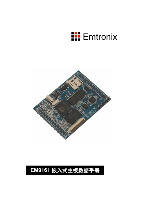
感谢您购买英创信息技术有限公司的产品:EM9161工控主板主板。
EM9161是一款面向工业自动化领域的高性价比嵌入式主板,其内核CPU为工业级品质的AT91SAM9261S,模块已预装正版Window CE5.0实时多任务操作系统,用户可直接使用Microsoft提供的著名免费软件开发工具eVC(+SP4)或微软的其他开发工具,在EM9161上直接开发应用程序。
英创公司针对EM9161提供了完整的接口低层驱动以及丰富的应用程序范例,用户可在此基础上方便、快速地开发出各种工控产品。
EM9161G是EM9161的增强型产品,其运行速度更快,各管脚功能与EM9161完全相同。
EM9161主要特点:●标准的Windows图形界面:EM9161带有工业标准的TFT彩色LCD及触摸屏接口,为客户提供高性能的人机界面。
●丰富的标准接口资源:作为一款高性能的嵌入式主板产品,EM9161带有多种标准接口,以满足不同应用需求。
这些接口包括:(1)以太网接口,支持标准WinSock以及基于WinSock的各类API;(2)4个标准异步串口;(3)2路USB HOST接口;(4)USB Device接口,支持ActiveSync方式对内部文件操作以及程序调试;(5)MicroSD卡接口,直接支持SD卡;(6)I2C总线;(7)32位GPIO;(8)CAN总线接口(可选);(9)精简ISA扩展总线。
●强大的应用开发工具:EM9161预装了微软的Windows CE操作系统,Windows CE是当前市场上最流行的实时多任务操作系统之一,微软针对CE的应用开发推出一系列完善的开发工具,eVC就是其中的代表,eVC是基于Visual C/C++发展的嵌入式版本,且可免费获取。
英创公司为EM9161的所有接口编写符合CE标准的驱动程序,因此用户可直接调用标准Windows API来操作各个通讯接口。
此外用户可利用微软工具链中所提供的远程维护工具或ActiveSync来对EM9161运行的程序进行调试,以及后续的产品维护。
食品添加剂国际编码系统中文版
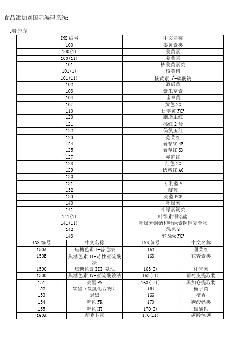
丽春红SX
127
赤鲜红
128
红色2G
129
诱惑红AC
130
131
专利蓝V
132
靛蓝
133
亮蓝FCF
140
叶绿素
141
叶绿素铜类
141(1)
叶绿素铜铭盐
141(11)
叶绿素铜钠和叶绿素铜钾复合物
142
绿色S
143
牢固绿FCF
INS编号
中文名称
INS编号
中文名称
150A
焦糖色素I-普通法
162
甜菜红
山梨醇和山梨醇糖浆
406
琼脂
421 (甜味剂)
甘露糖醇
407
卡拉胶
422 (保湿剂)
甘油
407A
加工过的麒麟海
424
热凝胶
408
焙烤酵母聚糖
425
魔芋粉
409
阿拉伯糖基半乳聚糖
410
角豆胶
411
燕麦胶
412
瓜尔豆胶
413
黄著爱尔兰
414
阿拉伯树胶
六,乳化剂、分散剂
INS编码
中文名称
INS编码
中文名称
335
酒石酸钠类
351(II)
苹果酸
335 (I)
酒后酸氢钠
352
苹果酸钙类
335 (II)
酒石酸钠
352 (I)
苹果酸氢钙
337
酒石酸钾钠
352
(II)
苹果酸钙
338
磷酸
353
偏酒石酸
339
磷酸钠类
354
酒石酸钙
mt9160be中文资料_数据手册_IC数据表

VBias VRef PWRST
Bias Voltage (Output). (VDD/2) volts is available at this pin for biasing external amplifiers. Connect 0.1 µF capacitor to VSSA,Connect 1 µF capacitor to Vref.
VSSD VDD VSSA
VBias VRef
Din Dout STB/F0i CLOCKin STBd/FOod (MT9161B only)
FILTER/CODEC GAIN ENCODER 7dB DECODER -7dB
Transducer Interface
Flexible Digital Interface
SCLK Serial Port Synchronous Clock (Input). Data clock for microport. CMOS level compatible.
DATA 1 Bidirectional Serial Data. Port for microprocessor serial data transfer. In Motorola/ National mode of operation, this pin becomes the data transmit pin only and data receive is performed on the DATA 2 pin. Input CMOS level compatible.
PWRST 4
20 HSPKR +
IC 5
19 HSPKR - A/µ/IRQ 6
18 VDD
VSSD 7
- 1、下载文档前请自行甄别文档内容的完整性,平台不提供额外的编辑、内容补充、找答案等附加服务。
- 2、"仅部分预览"的文档,不可在线预览部分如存在完整性等问题,可反馈申请退款(可完整预览的文档不适用该条件!)。
- 3、如文档侵犯您的权益,请联系客服反馈,我们会尽快为您处理(人工客服工作时间:9:00-18:30)。
400mA High PSRR, LDO RegulatorsFeaturesLow, 90µA No-Load Supply Current Guaranteed 400mA Output Current PSRR=65dB @ 120Hz; 55dB @ 1kHzOver-Temperature Protection and Short-CircuitProtectionOutput Voltage: 1.20V~5.00V (G9161-XXX) Stable with low cost ceramic capacitorsApplicationsCD ROM or DVD ROM DVD Player Audio CodecGeneral DescriptionThe G9161 series is a low supply current, high PSRR, and low dropout linear regulator that comes in a SOT-89, SOT-223, TO-252 and SOP-8 with Power PAD package. The supply current at no-load is 90µA. Operating voltage range is from 2.50V to 5.50V. The over-current protection limit is set at 550mA typical. An over- temperature protection circuit is built-in in the Device to prevent thermal overload. The output voltage range is from 1.2V to 5.0V.Ordering InformationORDER NUMBERMARKING VOLTAGETEMP. RANGE PACKAGE (Pb free)G9161-120T25U 9161AA 1.2V -40°C~ +85°C SOT-89 G9161-120T45U 9161-120 1.2V-40°C~ +85°C TO-252 G9161-120T65U 9161-120 1.2V-40°C~ +85°C SOT-223 G9161-120F1U 9161AA 1.2V -40°C~ +85°C SOP-8 (FD)For other output voltage, please contact us at sales@ Note: T2: SOT-89, T4: TO-252, T6: SOT-223, F1: SOP-8 (FD) 5: Bonding CodeU: Tape & ReelPin Configuration Typical Application CircuitIN GND IN GND SOT-89、SOT-223OUTµFIN OUTTO-252OUTOUT OUTSOP-8 (FD)NC/GND NC/GND GNDNC/GNDNote: Recommend connecting the Thermal Pad to the GND for excellent power dissipation.ORDER NUMBER OUTPUT VOLTAGE (V) MARKINGG9161-120T25U 1.20 9161AA G9161-130T25U 1.30 9161AB G9161-140T25U 1.40 9161AC G9161-150T25U 1.50 9161AD G9161-160T25U 1.60 9161AE G9161-170T25U 1.70 9161AF G9161-180T25U 1.80 9161AG G9161-190T25U 1.90 9161AH G9161-200T25U 2.00 9161AI G9161-210T25U 2.10 9161AJ G9161-220T25U 2.20 9161AK G9161-230T25U 2.30 9161AL G9161-240T25U 2.40 9161AM G9161-250T25U 2.50 9161AN G9161-260T25U 2.60 9161AO G9161-270T25U 2.70 9161AP G9161-280T25U 2.80 9161AQ G9161-285T25U 2.85 9161AR G9161-290T25U 2.90 9161AS G9161-300T25U 3.00 9161AT G9161-310T25U 3.10 9161AU G9161-315T25U 3.15 9161AV G9161-320T25U 3.20 9161AW G9161-330T25U 3.30 9161AX G9161-340T25U 3.40 9161AY G9161-350T25U 3.50 9161AZ G9161-360T25U 3.60 9161BA G9161-370T25U 3.70 9161BB G9161-380T25U 3.80 9161BC G9161-390T25U 3.90 9161BD G9161-400T25U 4.00 9161BE G9161-410T25U 4.10 9161BF G9161-420T25U 4.20 9161BG G9161-430T25U 4.30 9161BH G9161-440T25U 4.40 9161BI G9161-450T25U 4.50 9161BJ G9161-460T25U 4.60 9161BK G9161-470T25U 4.70 9161BL G9161-475T25U 4.75 9161BM G9161-480T25U 4.80 9161BN G9161-490T25U 4.90 9161BO G9161-500T25U 5.00 9161BP T2: SOT-89ORDER NUMBER OUTPUT VOLTAGE (V) MARKINGG9161-120T45U 1.20 9161-120 G9161-130T45U 1.30 9161-130 G9161-140T45U 1.40 9161-140 G9161-150T45U 1.50 9161-150 G9161-160T45U 1.60 9161-160 G9161-170T45U 1.70 9161-170 G9161-180T45U 1.80 9161-180 G9161-190T45U 1.90 9161-190 G9161-200T45U 2.00 9161-200 G9161-210T45U 2.10 9161-210 G9161-220T45U 2.20 9161-220 G9161-230T45U 2.30 9161-230 G9161-240T45U 2.40 9161-240 G9161-250T45U 2.50 9161-250 G9161-260T45U 2.60 9161-260 G9161-270T45U 2.70 9161-270 G9161-280T45U 2.80 9161-280 G9161-285T45U 2.85 9161-285 G9161-290T45U 2.90 9161-290 G9161-300T45U 3.00 9161-300 G9161-310T45U 3.10 9161-310 G9161-315T45U 3.15 9161-315 G9161-320T45U 3.20 9161-320 G9161-330T45U 3.30 9161-330 G9161-340T45U 3.40 9161-340 G9161-350T45U 3.50 9161-350 G9161-360T45U 3.60 9161-360 G9161-370T45U 3.70 9161-370 G9161-380T45U 3.80 9161-380 G9161-390T45U 3.90 9161-390 G9161-400T45U 4.00 9161-400 G9161-410T45U 4.10 9161-410 G9161-420T45U 4.20 9161-420 G9161-430T45U 4.30 9161-430 G9161-440T45U 4.40 9161-440 G9161-450T45U 4.50 9161-450 G9161-460T45U 4.60 9161-460 G9161-470T45U 4.70 9161-470 G9161-475T45U 4.75 9161-475 G9161-480T45U 4.80 9161-480 G9161-490T45U 4.90 9161-490 G9161-500T45U 5.00 9161-500 T4: TO-252ORDER NUMBER OUTPUT VOLTAGE (V) MARKINGG9161-120T65U 1.20 9161-120 G9161-130T65U 1.30 9161-130 G9161-140T65U 1.40 9161-140 G9161-150T65U 1.50 9161-150 G9161-160T65U 1.60 9161-160 G9161-170T65U 1.70 9161-170 G9161-180T65U 1.80 9161-180 G9161-190T65U 1.90 9161-190 G9161-200T65U 2.00 9161-200 G9161-210T65U 2.10 9161-210 G9161-220T65U 2.20 9161-220 G9161-230T65U 2.30 9161-230 G9161-240T65U 2.40 9161-240 G9161-250T65U 2.50 9161-250 G9161-260T65U 2.60 9161-260 G9161-270T65U 2.70 9161-270 G9161-280T65U 2.80 9161-280 G9161-285T65U 2.85 9161-285 G9161-290T65U 2.90 9161-290 G9161-300T65U 3.00 9161-300 G9161-310T65U 3.10 9161-310 G9161-315T65U 3.15 9161-315 G9161-320T65U 3.20 9161-320 G9161-330T65U 3.30 9161-330 G9161-340T65U 3.40 9161-340 G9161-350T65U 3.50 9161-350 G9161-360T65U 3.60 9161-360 G9161-370T65U 3.70 9161-370 G9161-380T65U 3.80 9161-380 G9161-390T65U 3.90 9161-390 G9161-400T65U 4.00 9161-400 G9161-410T65U 4.10 9161-410 G9161-420T65U 4.20 9161-420 G9161-430T65U 4.30 9161-430 G9161-440T65U 4.40 9161-440 G9161-450T65U 4.50 9161-450 G9161-460T65U 4.60 9161-460 G9161-470T65U 4.70 9161-470 G9161-475T65U 4.75 9161-475 G9161-480T65U 4.80 9161-480 G9161-490T65U 4.90 9161-490 G9161-500T65U 5.00 9161-500 T6: SOT-223ORDER NUMBER OUTPUT VOLTAGE (V) MARKINGG9161-120F1U 1.20 9161AA G9161-130 F1U 1.30 9161ABG9161-140 F1U 1.40 9161ACG9161-150 F1U 1.50 9161ADG9161-160 F1U 1.60 9161AEG9161-170 F1U 1.70 9161AFG9161-180 F1U 1.80 9161AGG9161-190 F1U 1.90 9161AHG9161-200 F1U 2.00 9161AIG9161-210 F1U 2.10 9161AJG9161-220F1U 2.20 9161AK G9161-230F1U 2.30 9161AL G9161-240F1U 2.40 9161AM G9161-250F1U 2.50 9161AN G9161-260F1U 2.60 9161AO G9161-270F1U 2.70 9161AP G9161-280F1U 2.80 9161AQ G9161-285F1U 2.85 9161AR G9161-290F1U 2.90 9161AS G9161-300 F1U 3.00 9161ATG9161-310 F1U 3.10 9161AUG9161-315 F1U 3.15 9161AVG9161-320 F1U 3.20 9161AWG9161-330 F1U 3.30 9161AXG9161-340 F1U 3.40 9161AYG9161-350 F1U 3.50 9161AZG9161-360 F1U 3.60 9161BAG9161-370 F1U 3.70 9161BBG9161-380 F1U 3.80 9161BCG9161-390 F1U 3.90 9161BDG9161-400 F1U 4.00 9161BEG9161-410 F1U 4.10 9161BFG9161-420 F1U 4.20 9161BGG9161-430 F1U 4.30 9161BHG9161-440 F1U 4.40 9161BIG9161-450 F1U 4.50 9161BJG9161-460 F1U 4.60 9161BKG9161-470 F1U 4.70 9161BLG9161-475 F1U 4.75 9161BMG9161-480 F1U 4.80 9161BNG9161-490 F1U 4.90 9161BOG9161-500 F1U 5.00 9161BPF1: SOP-8 (FD)Absolute Maximum RatingsInput Voltage. . . . . . . . . . . . . . . . . . . . . . . . . . . . . . . .7V Power Dissipation Internally LimitedMaximum Junction Temperature. . . . . . . . . . . . .150°C Storage Temperature Range . . . .-65°C ≤ T J ≤+150°C Reflow Temperature (soldering, 10sec) . . . . . .260°C Thermal Resistance Junction to Ambient, (θJA ) (1)SOT-89. . . . . . . . . . . . . . . . . . . . . . . . . . . . . . 153°C/W TO-252. . . . . . . . . . . . . . . . . . . . . . . . . . . . . . 102°C/W SOT-223. . . . . . . . . . . . . . . . . . . . . . . . . . . . . 118°C/W SOP-8 (FD) . . . . . . . . . . . . . . . . . . . . . . . . . . 162°C/W Thermal Resistance Junction to Case, (θJc )SOT-89 . . . . . . . . . . . . . . . . . . . . . . . . . . . . . .. 48°C/W TO-252. . . . . . . . . . . . . . . . . . . . . . . . . . . . . . . ..8°C/W SOT-223. . . . . . . . . . . . . . . . . . . . . . . . . . . . . .20°C/W SOP-8 (FD) . . . . . . . . . . . . . . . . . . . . . . . . . . . 12°C/WNote (1): See Recommended Minimum Footprint.Operating Conditions (Note 1)Input Voltage. . . . . . . . . . . . . . . . . . . . . . . . .2.5V ~ 5.5V Temperature Range. . . . . . . . . . . . . .-40°C ≤ T A ≤85°CElectrical Characteristics(V IN =+3.6V, T A =T J =+25°C, C IN =4.7µF, C OUT =4.7µF, unless otherwise noted.) (Note 1)PARAMETER SYMBOLCONDITION MIN TYP MAX UNITInput Voltage (Note 2) V IN 2.5 --- 5.5V V OUT ≥2.50V, I OUT =1mA-2 --- 2 2.50V>V OUT ≥1.80V, I OUT =1mA -3 --- 3 Output Voltage Accuracy V OUT 1.80V>V OUT ≥1.20V, I OUT =1mA-4 --- 4 % Maximum Output Current 400 --- ---mA Current Limit (Note 4) I LIM 400 550 ---mAShort Circuit Current Isc---280---mA Ground Pin CurrentI Q--- 90 ---µAV OUT =1.20V --- 22.3V OUT = 1.80V --- 1.4 1.7V OUT =2.50V --- 0.8 1 Dropout Voltage (Note 5)V DROPI OUT =400mAV OUT =3.30V --- 0.48 0.67VLine Regulation ΔV LNR SET=GND, V IN =V (STD)+0.1V,to 6.2VI OUT =10mA--- 0.06 0.12%/VLoad Regulation ΔV LDR I OUT =10mA to 400mA------0.02%/mARipple Rejection PSRRF=120Hz, 0.49V P-P , I OUT =10mA --- 65 ---dBThermal ProtectionThermal Shutdown Temperature T SHDN --- 145 ---°CThermal Shutdown HysteresisΔT SHDN--- 25 ---°CNote 1: Limits is 100% production tested at T A = +25°C. Low duty pulse techniques are used during test to maintain junc-tion temperature as close to ambient as possible.Note 2: Guaranteed by line regulation test. Note 3: Adjustable mode only.Note 4: Not tested. For design purposes, the current limit should be considered 400mA minimum to 650mA maximum.Note 5: The dropout voltage is defined as (V IN -V OUT ) when V OUT is 100mV below the target value of V OUT . The performance ofevery G9161 part, see “Typical Performance Characteristics ”.Typical Performance Characteristics(V IN=3.6V, V OUT=1.2V, C IN=4.7µF, C OUT=4.7µF, T A=25°C, unless otherwise noted.)Line Transient Response Load Transient Response Short Circuit CurrentOvercurrent Protection Characteristics Start-upSOT-223 Max. Power DissipationSOT-223 Max. Power DissipationSOT-89 Max. Power Dissipation SOT-89 Max. Power DissipationTO-252 Max. Power Dissipation TO-252 Max. Power DissipationOutput Voltage vs. ISOP-8 Max. Power Dissipation SOP-8 Max. Power DissipationRecommended Minimum FootprintRecommended Ground Layout for Power DissipationSOT-89SOT-223TO-252SOP-8 (FD)SOP-8 (FD)Pin DescriptionPIN NAMEFUNCTIONSOT-89 TO-252 SOT-223SOP-8 (FD)1 1 1 1,2 INRegulator Input. Supply voltage can range from +2.5V to +5.5V. By-pass with 1µF to GND2 2 2 6 GNDGround. This pin also functions as a heatsink. Solder to large pads orthe circuit board ground plane to maximize thermal dissipation.3 3 3 3,4 OUTRegulator Output. Sources up to 300mA. Bypass with a 1µF, <0.2Ωtypical ESR capacitor to GND.5,7,8NC/GND Connect to GND for heatsink.Thermal PadRecommend connecting the Thermal Pad to the GND for excellentpower dissipation.Detailed DescriptionOver Current ProtectionThe G9161 uses a current sense-resistor to monitor the output current. A portion of the PMOS output tran-sistor’s current is mirrored to a resistor such that the voltage across this resistor is proportional to the output current. Once the output current exceeds limit thresh-old, G9161 would be protected with a limited output current. Further more, when the output is short to ground, the output current would be folded-back to a less limit.Over Temperature ProtectionTo prevent abnormal temperature from occurring, the G9161 has a built-in temperature monitoring circuit. When it detects the temperature is above 145°C, the output transistor is turned off. When the IC is cooled down to below 120°C, the output is turned on again. In this way, the G9161 will be protected against abnor-mal junction temperature during operation.Applications InformationCapacitor Selection and Regulator StabilityNormally, use a 1µF capacitor on the input and a 1µF capacitor on the output of the G9161. Larger input capacitor values and lower ESR provide better sup-ply-noise rejection and transient response. A higher- value input capacitor (10µF) may be necessary if large, fast transients are anticipated and the device is lo-cated several inches from the power source.Power-Supply Rejection and Operation from Sources Other than BatteriesThe G9161 is designed to deliver low dropout voltages and low quiescent currents in battery powered sys-tems. Power-supply rejection is 65dB at low frequen-cies. As the frequency increases above 20kHz, the output capacitor is the major contributor to the rejec-tion of power-supply noise.When operating from sources other than batteries, improve supply-noise rejection and transient response by increasing the values of the input and output ca-pacitors, and using passive filtering techniques. Load Transient ConsiderationsThe G9161 load-transient response graphs show two components of the output response: a DC shift of the output voltage due to the different load currents, and the transient response. Typical overshoot for step changes in the load current from 10mA to 300mA is 8mV. Increasing the output capacitor 's value and de-creasing its ESR attenuates transient spikes.Input-Output (Dropout) VoltageA regulator 's minimum input-output voltage differential (or dropout voltage) determines the lowest usable sup-ply voltage. In battery-powered systems, this will de-termine the useful end-of-life battery voltage. Because the G9161 use a P-channel MOSFET pass transistor, their dropout voltage is a function of R DS(ON) multiplied by the load current.Package InformationSOT-89 (T2) PackageDIMENSIONS IN MILLIMETER DIMENSIONS IN INCH SYMBOLMIN NOM MAX MIN NOM MAXA 1.40 1.50 1.60 0.055 0.059 0.063 A1 0.80 1.04 ----- 0.031 0.041 -----b 0.36 0.42 0.48 0.014 0.016 0.018 b1 0.41 0.47 0.53 0.016 0.0180.020 C 038 0.40 0.43 0.014 0.015 0.017 D 4.40 4.50 4.60 0.173 0.177 0.181 D1 1.40 1.60 1.75 0.055 0.062 0.069 HE ----- ----- 4.25 ----- ----- 0.167 E 2.40 2.50 2.60 0.094 0.098 0.102 e 2.90 3.00 3.10 0.114 0.118 0.122TO-252 (T4) PackageMILLIMETERS INCHES SYMBOLMIN. MAX. MIN. MAX.A 2.19 2.38 0.086 0.094 A1 0.89 1.27 0.035 0.050 b 0.64 0.89 0.025 0.035 C 0.46 0.58 0.018 0.023 D 5.97 6.22 0.235 0.245 E 6.35 6.73 0.2500.265 E1 5.21 5.46 0.205 0.215 e 2.26BSC0.09BSC e1 3.96 5.18 0.156 0.204 F 0.46 0.58 0.018 0.023 L1 0.89 2.03 0.035 0.080 L2 0.64 1.02 0.025 0.040 L3 2.40 2.80 0.095 0.110 H 9.40 10.40 0.370 0.410 θ 0° 4° 0° 4°SOT-223 (T6) PackageMILLIMETER INCH SYMBOLMIN MAX MIN MAXA 1.55 1.80 0.061 0.071 A1 0.02 0.12 0.0008 0.0047B 0.60 0.80 0.024 0.031 B1 2.90 3.10 0.1140.122 C 0.24 0.32 0.009 0.013 D 6.30 6.70 0.248 0.264 E 3.30 3.70 0.130 0.146 e 2.30 BSC 0.090 BSC e1 4.60 BSC 0.181 BSC H 6.70 7.30 0.264 0.287 L 0.90 MIN 0.036 MIN L2 0.06 BSC0.0024 BSCα0° 10°0° 10°°(4X)α(4X)SOP-8 (FD) PackageNote:1. JEDEC Outline: MS-012 AA/E.P. Version: N/A2. Dimension “D” does not include mold flash, protrusions or gate burrs. Mold flash, protrusions and gate burrs shall not ex-ceed .15mm (.006in) per side.3. Dimensions “E” does not include inter-lead flash, or protrusions inter-lead flash and protrusions shall not exceed .25mm(.010in) per side.DIMENSION IN MM DIMENSION IN INCHSYMBOLMIN. MAX. MIN. MAX.A1.397 1.753 0.053 0.069A1 0.00 0.13 0.000 0.005 A2 1.40 TYP 0.055 TYPB0.330 0.508 0.013 0.020D4.8015.004 0.189 0.197E3.810 3.988 0.150 0.157e 1.27 TYP 0.05 TYPH5.7916.198 0.228 0.244L0.508 0.711 0.020 0.028θ0°8°0°8°D13.048 3.556. 0.120 0.140E12.159 2.667 0.085 0.105 Taping SpecificationPACKAGE Q’TY/BY REELSOT-89 1,000eaTO-252 2,500eaSOT-223 2,500eaSOP-8 (FD) 2,500 eaGMT Inc. does not assume any responsibility for use of any circuitry described, no circuit patent licenses are implied and GMT Inc. reserves the right at any time without notice to change said circuitry and specifications.BSOT-89、223 Package Orientation TO-252 Package Orientation Typical SOP Package Orientation。