MAX5090CATE+中文资料
MAX3096CPE中文资料

DC ELECTRICAL CHARACTERISTICS—MAX3095
(VCC = 5V ±5%, TA = TMIN to TMAX, unless otherwise noted. Typical values are at TA = +25°C.) (Note 1) PARAMETER Receiver Differential Input Threshold Receiver Input Hysteresis Receiver Input Current (A_, B_) Enable Input Current (G, G) Enable Input High Voltage (G, G) Enable Input Low Voltage (G, G) Receiver Output High Voltage Receiver Output Low Voltage Three-State Current at Receiver Output Output Short-Circuit Current Receiver Input Resistance Supply Current ESD Protection (Note 2) VIH VIL VOH VOL IOZR IOSR RIN ICC IOUT = -4mA, VID = 200mV, G = VCC or G = GND, Figure 1 IOUT = 4mA, VID = -200mV, G = VCC or G = GND, Figure 1 0 ≤ VOUT ≤ VCC, G = GND and G = VCC 0 ≤ VOUT ≤ VCC, G = VCC or G = GND -7V ≤ VCM ≤ 12V No load, G = VCC or G = GND G = GND and G = VCC Human Body Model IEC1000-4-2 (Air-Gap Discharge) IEC1000-4-2 (Contact Discharge) ±7 48 2.4 0.001 ±15 ±15 ±8 kV 3.5 10 VCC - 1.5 0.4 ±1 ±75 2.0 0.8 IIN SYMBOL VTH CONDITIONS -7V ≤ VCM ≤ 12V VCM = 0 VCC = 0 or 5.25V VIN = 12V VIN = -7V MIN -200 45 250 -200 ±1 TYP MAX 200 UNITS mV mV µA µA V V V V µA mA kΩ mA µA
CAT9555中文资料

概述CAT9555是一款基于COMS工艺的器件,它提供了I2C和SMBus在应用中的16位通用并行输入、输出口的扩展。
当应用中需要额外的I/O口来连接传感器、电源开关、LED、按钮、风扇等时,可使用I/O扩展器件实现简单的解决方案。
CAT9555包含两个8位配置寄存器(输入或输出选择)、输入寄存器、输出寄存器、极性反转寄存器和一路兼容I2C/SMBus串行接口。
通过写配置寄存器可将16个I/O口中的任何一个配置成为输入或输出。
系统主控制器可以通过写高电平有效的极性反转寄存器将CAT9555的输入数据反转。
当任何输入口状态改变时,CAT9555就会产生一个低电平中断,该中断可以用来向系统主控器指明输入端口状态的改变。
CAT9555有3个输入管脚来实现扩充I2C地址,最多允许8个器件共用在一个I2C/SMBus总线上。
CAT9555固定的I2C地址与CAT9554相同,只允许8个器件连接接到同一个I2C/SMBus总线上。
特性兼容400KHz I2C总线工作电源电压:2.3V~5.5V低待机电流I/O口可承受5V电压16个I/O口,默认为16个高电平输入口高驱动能力独立的输入输出配置寄存器极性反转寄存器低电平有效中断输出内部上电复位上电时无干扰脉冲信号SCL/SDA输入的噪声滤波器可级联8个器件工业级温度范围提供三种不同的封装形式:与RoHS兼容的24脚SOIC、TSSOP封装和24脚的TQFN封装(4mmx4mm)定制信息结构框图SOIC/TSSOP1234-111213-2021222324应用场合白色电器(洗碗机和洗衣机)手持设备(手机、PDA和数码相机)数据通信(路由器、集线器和服务器)。
MAX485中文资料
本文是Maxim 正式英文资料的译文,Maxim 不对翻译中存在的差异或由此产生的错误负责。
请注意译文中可能存在文字组织或翻译错误,如需确认任何词语的准确性,请参考Maxim 提供的英文版资料。
索取免费样品和最新版的数据资料,请访问Maxim 的主页: 。
_______________________________概述MAX481、MAX483、MAX485、MAX487-MAX491以及MAX1487是用于RS-485与RS-422通信的低功耗收发器,每个器件中都具有一个驱动器和一个接收器。
MAX483、MAX487、MAX488以及MAX489具有限摆率驱动器,可以减小EMI ,并降低由不恰当的终端匹配电缆引起的反射,实现最高250k b p s 的无差错数据传输。
M A X 481、MAX485、MAX490、MAX491、MAX1487的驱动器摆率不受限制,可以实现最高2.5Mbps 的传输速率。
这些收发器在驱动器禁用的空载或满载状态下,吸取的电源电流在120(A 至500(A 之间。
另外,MAX481、MAX483与MAX487具有低电流关断模式,仅消耗0.1µA 。
所有器件都工作在5V 单电源下。
驱动器具有短路电流限制,并可以通过热关断电路将驱动器输出置为高阻状态,防止过度的功率损耗。
接收器输入具有失效保护特性,当输入开路时,可以确保逻辑高电平输出。
MAX487与MAX1487具有四分之一单位负载的接收器输入阻抗,使得总线上最多可以有128个M A X 487/MAX1487收发器。
使用MAX488-MAX491可以实现全双工通信,而MAX481、MAX483、MAX485、MAX487与MAX1487则为半双工应用设计。
_______________________________应用低功耗RS-485收发器低功耗RS-422收发器电平转换器用于EMI 敏感应用的收发器工业控制局域网____________________下一代器件的特性♦容错应用MAX3430: ±80V 故障保护、失效保护、1/4单位负载、+3.3V 、RS-485收发器MAX3440E-MAX3444E: ±15kV ESD 保护、±60V 故障保护、10Mbps 、失效保护、RS-485/J1708收发器♦对于空间受限应用MAX3460-MAX3464: +5V 、失效保护、20Mbps 、Profibus RS-485/RS-422收发器MAX3362: +3.3V 、高速、RS-485/RS-422收发器,采用SOT23封装MAX3280E-MAX3284E: ±15kV ESD 保护、52Mbps 、+3V 至+5.5V 、SOT23、RS-485/RS-422、真失效保护接收器MAX3293/MAX3294/MAX3295: 20Mbps 、+3.3V 、SOT23、RS-485/RS-422发送器♦对于多通道收发器应用MAX3030E-MAX3033E: ±15kV ESD 保护、+3.3V 、四路RS-422发送器♦对于失效保护应用MAX3080-MAX3089: 失效保护、高速(10Mbps)、限摆率RS-485/RS-422收发器♦对于低电压应用MAX3483E/MAX3485E/MAX3486E/MAX3488E/MAX3490E/MAX3491E: +3.3V 供电、±15kV ESD 保护、12Mbps 、限摆率、真正的RS-485/RS-422收发器MAX481/MAX483/MAX485/MAX487–MAX491/MAX1487低功耗、限摆率、RS-485/RS-422收发器_____________________________________________________________________选择表19-0122; Rev 8; 10/03定购信息在本资料的最后给出。
1.5KE510CA中文资料

1.5KE510CA中文资料The 1.5KE Series is designed specifically to protect sensitive electronics equipment from voltage transients induced by lightning and other transient voltage events. These devices are ideal for the protection of I/O interfaces, Vcc bus and other vulnerable circuits used in telecom, computer, industrial and consumer electronic applications.FEATURESRoHS Compliant6.8V to 550VoltsUni-directional and Bi-directionalGlass passivated chip junction in DO-201 package1500W surge capability at 10/1000μs wave formExcellent clamping capabilityLow zener impedance to BV min.Typical IR less than 1μA above 10V, (9.5mm) lead length,5lbs., (2.3kg) tensionAgency Approvals:Recognized under the Components Program of Underwriters Laboratories.Agency File Number:E128662MAXIMUM RATINGS AND CHARACTERISTICS @25?C AMBIENT TEMPERATURE (unless otherwise noted)RATINGPeak Pulse Power Dissipation atT A=25?C, T P=1ms(Note 1)Steady State Power Dissipation at T L=75?C, Leadlengths .375", (9.5mm) (Note 2)Superimposed on Rated Load, (JEDEC Method) (Note 3) Operating junction and Storage Temperature RangeVALUEMin15006.5200-55 to +175UNITWattsWattsAmps°C SYMBOLP PPMP M(AV)I FSMT j, T STGNotes:1. Non-repetitive current pulse, per Fig.3 and derated above T A= 25?C per Fig.23. 8.3 ms single half sine-wave, or equivalent square wave, Duty cycle= 4 pulses per minutes maximum.Mechanical Specifications:Weight:0.045 ounce, 1.2 gramsCase:JEDEC DO-201 Molded plastic Mounting Position:Any Polarity:Color band denotes cathodeexcept BipolarTerminal:Axial leads, solderable per MIL-STD-750,Method 20266S I L I C O N D I O D E A R R A Y SBreakdown Voltage V BR (Volts) @ I T Maximum Reverse Leakage I R @ V R (μA)Maximum Clamping Voltage V C @ I PP (Volts)Maximum Peak Pulse Current I PP (A)ELECTRICAL SPECIFICATION @ Tamb 25°C1.5KE6.8A 1.5KE6.8CA 5.80 6.457.141010.5144.810001.5KE7.5A 1.5KE7.5CA6.407.137.881011.3134.55001.5KE8.2A 1.5KE8.2CA7.027.798.611012.1125.62001.5KE9.1A 1.5KE9.1CA 7.788.659.50113.4113.4501.5KE10A 1.5KE10CA 8.559.5010.50114.5104.8101.5KE11A 1.5KE11CA 9.4010.5011.60115.697.451.5KE12A 1.5KE12CA 10.2011.4012.60116.791.051.5KE13A 1.5KE13CA11.1012.4013.70118.283.551.5KE15A 1.5KE15CA12.8014.3015.80121.271.751.5KE16A 1.5KE16CA13.6015.2016.80122.567.651.5KE18A 1.5KE18CA 15.3017.1018.90125.260.351.5KE20A 1.5KE20CA 17.1019.0021.00127.754.951.5KE22A 1.5KE22CA 18.8020.9023.10130.649.751.5KE24A 1.5KE24CA 20.5022.8025.20133.245.851.5KE27A 1.5KE27CA 23.1025.7028.40137.540.551.5KE30A 1.5KE30CA 25.6028.5031.50141.436.751.5KE33A 1.5KE33CA 28.2031.4034.70145.733.351.5KE36A 1.5KE36CA 30.8034.2037.80149.930.551.5KE39A 1.5KE39CA 33.3037.1041.00153.928.251.5KE43A 1.5KE43CA36.8040.9045.20159.325.651.5KE47A 1.5KE47CA 40.2044.7049.40164.823.551.5KE51A 1.5KE51CA 43.6048.5053.60170.121.751.5KE56A 1.5KE56CA 47.8053.2058.80177.019.751.5KE62A 1.5KE62CA 53.0058.9065.10185.017.951.5KE68A 1.5KE68CA 58.1064.6071.40192.016.551.5KE75A 1.5KE75CA 64.1071.3078.801103.014.851.5KE82A 1.5KE82CA 70.1077.9086.101113.013.551.5KE91A 1.5KE91CA 77.8086.5095.501125.012.251.5KE100A 1.5KE100CA 85.5095.00105.001137.011.151.5KE110A 1.5KE110CA 94.00105.00116.001152.010.051.5KE120A 1.5KE120CA 102.00114.00126.001165.09.251.5KE130A 1.5KE130CA 111.00124.00137.001179.08.551.5KE150A 1.5KE150CA 128.00143.00158.001207.07.351.5KE160A 1.5KE160CA 136.00152.00168.001219.0 6.951.5KE170A 1.5KE170CA 145.00162.00179.001234.0 6.551.5KE180A 1.5KE180CA 154.00171.00189.001246.0 6.251.5KE200A 1.5KE200CA 171.00190.00210.001274.0 5.551.5KE220A 1.5KE220CA 185.00209.00231.001328.0 4.651.5KE250A 1.5KE250CA 214.00237.00263.001344.0 4.451.5KE300A 1.5KE300CA 256.00285.00315.001414.0 3.751.5KE350A 1.5KE350CA 300.00332.00368.001482.0 3.251.5KE400A 1.5KE400CA 342.00380.00420.001548.0 2.851.5KE440A 1.5KE440CA 376.00418.00462.001602.0 2.551.5KE480A 1.5KE480CA 408.00456.00504.001658.0 2.351.5KE510A 1.5KE510CA 434.00485.00535.001698.0 2.151.5KE530A 1.5KE530CA 450.00503.50556.501725.0 2.151.5KE540A 1.5KE540CA 459.00513.00567.001740.0 2.051.5KE550A1.5KE550CA467.00522.50577.501760.02.05Reverse Stand off Voltage V R (Volts)For bidirectional type having Vrwm of 10 volts and less, the IR limit is double.For parts without A , the VBR is +10%Test Current I T (mA)MIN MAX Part NumbersUni-Polar Bi-PolarFig. 1 Peak Pulse Power Rating Curve Fig. 2 Pulse Derating Curve Fig. 3 Pulse WaveformIPPM-PeakPuleCurrent,%IRSM0 1.0 2.0 3.0 4.0t-Time (ms)Fig. 4- Typical Junction Capacitance CJ-Capacitane(pF)51010100500VWM-Reverse Stand-Off Voltage (V) Fig. 6- Maximum Non-Repetitive Forward Surge Current Uni-Directional OnlyIFSM-PeakForwardSugeCurrent(A)20010010Number of Cylces at 60HZ Fig. 5 Steady State Power Derating CurveT L- Lead Temperature (?C)SteadyStatePwerDissipation(W)02550753.0 100125150175200 PPPM-PeakulsePower(kW)0.1s 1.0s10s100s 1.0ms10ms0.1110100t d- Pulse Width (sec.)T A- Ambient Temperature (?C) PeakPulsePw e r ( P P P ) o r C u r r e n t ( I P P ) D e r a t i ninPercentage,%252550507575100100125150175200 Ratings and Characteristic Curves T A=25?C unless otherwise noted6S I L I C O N D I O D E A R R A Y SOutline DimensionsCase Style 1.5KE(DO-201)Dimensions in inches and (millimeters)。
MAX3490摘出资料(部分中文)
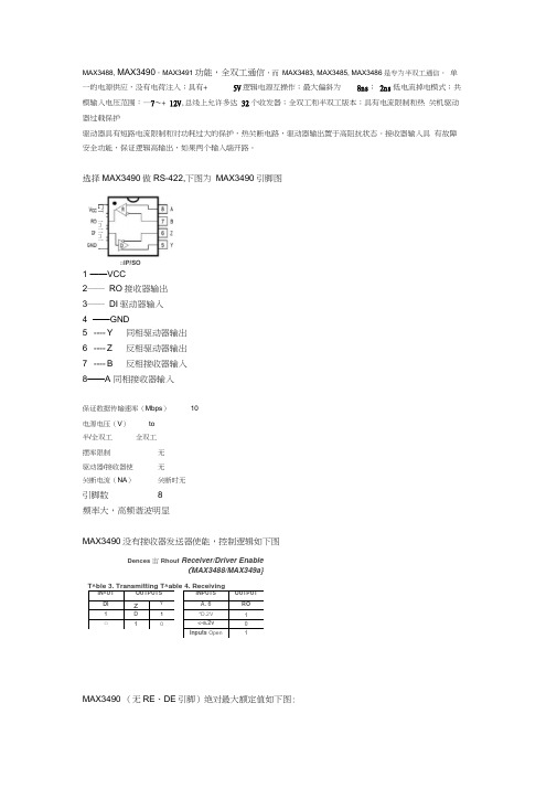
MAX3488, MAX3490,MAX3491 功能,全双工通信,而 MAX3483, MAX3485, MAX3486是专为半双工通信。
单一的电源供应,没有电荷注入;具有+ 5V 逻辑电源互操作;最大偏斜为 8ns ; 2ns 低电流掉电模式;共模输入电压范围:—7〜+ 12V ,总线上允许多达 32个收发器;全双工和半双工版本;具有电流限制和热 关机驱动器过载保护驱动器具有短路电流限制和对功耗过大的保护,热关断电路,驱动器输岀置于高阻抗状态。
接收器输入具 有故障安全功能,保证逻辑高输岀,如果两个输入端开路。
选择MAX3490做RS-422,下图为 MAX3490引脚图1 ——VCC2―― RO 接收器输出 3―― DI 驱动器输入 4 ——GND 5 ---- Y 同相驱动器输出 6 ---- Z 反相驱动器输出 7 ---- B反相接收器输入8——A 同相接收器输入保证数据传输速率(Mbps ) 10电源电压(V ) to 半/全双工 全双工摆率限制 无 驱动器/接收器使 无 关断电流(NA )关断时无引脚数8频率大,高频谐波明显MAX3490没有接收器发送器使能,控制逻辑如下图Dences 宙Rhouf Receiver/Driver Enable(MAX3488/MAX349a}T^ble 3. Transmitting T^able 4. ReceivingMAX3490 (无RE 、DE 引脚)绝对最大额定值如下图:IN^UTOUTPUTSDI zY 1 D 1 □1INPUTSOUTPUTA. 6 RO *D.2V1 <-a.2v0 Inputs Open1□IP/SOE L叵叵DABSOLUTE MAXIMUM RATINGSS U P P 卜F \ 01 ^3 9 e l\/ kill ■ ■ ■ ■ ■■!■■■■■■ iri ■ ■ ■ ■ ■ ■ ■ ■ ■ ■ ■ ■■ ■ ■ ■ ■ ■ i ■ ■ ■ r ■ ■ ■ ■ ■ ■ ■Control IrpiJ ValLage (RE, D£) ............... .......... ............... -0.3V ta 7V□rtvsr Inpul Voltage (6l).............. .......... .......... ............... -0.3Vtn 7VOnvar Output VcItaQ* (A,気V, ZX - ......................... -7J5V to12.SVftccer^CF Input VaKagc |A, B) . -7.5V to )2 5VReceiver Ojtput Voltage (RO) . . -O.3Vto (Vcc * 0 3V)Gontinucus Power g$ipmTk?n (T R= +70芒|各Pin Pi/Mc DIP 忖申rate 9 09mWU above +70© 72?mW8-Pin SO (<1HW 5 aarrrtVy «bove +7C P C), 471mW14-Rn Plastic DlP(de<m© 10mW fl C above +70忙》... HOOtrMf14-Rn SO (deia1^ fl.SSmW.^C abaw +70*C> __________ UUJllMfOperating Temperalur?MAXU C .............. ......... *........ ... ..................... -.Ot:to +7[TCMAX3d_ _E__”…lh.. “一,. ,.H.…““-“,-H.⑷乜B +85\:Storage Temperafur? Range lo +16[yCbead Tempeiature [wldering lOlMC)..................................... +XD*CMAX3490驱动器的开关特性如下图:DRIVER SWITCHING CHARACTERISTICS-MAX3465h MAX14$0, and MAX3491ri^E:» 3.3M a T*w *25*CJPARAMtFER CONCilTICNS m TVP MA 9(UNITSDrrwf OHtreftfiii OdljMjt Del叩g■ Sdll, Figure 7 122M mDrvcr Wfe-oEiii Ckrlp ui T M7»C r Time hno良L * fiOtl, Flpm 71&25mEtr p临他n M■丫LCfflMCHHiah Lrvtl IpiLM R L * 37(1. F4l/*a T2235m轉、ion Delay Hl0hi&-Lew Leveli IpML R. - ZTflFiflWWE■Jr22 35tp L n - iPHitl □越g*曲m Dtt&Ff吕的却iH^ie S- IPDS R.fc• 27n, FipL<eS E mDRIVER OUTPUT ENABLEJOIS^BLE TIMES {IWS-iflS'IMLW3-431 聞切Dmw CXJtput tnable r me I Q L OW LE^el tfZL Ri= 110SL f^FLFa 10 45 M OEDiwci" OulpiJl EiwN? Trne tg High Len el S FZH Ri ■ 110(1 钿ure $ 45raDrw CMp讥04»^le Time tom Migih Level fi t* 11(X1. F»flL*t940 to POriw D・*l・ Tim from LwLwi tpLE R L* 11IMI. i&40 BO mDTM< dip Lit Errtb^A Tiffii Au墟电叭旳Lx L#v4l tm Rl ■匚如i 10<8W gm 他Qrta&r ErrtBifi Titre frw 电靜©询|a H(;h 4PCH R; - 1inni FigiLiraS®o r»MAX3490CPA(TCto +70'Q8 Ptasttc DIPMAX349OCSA(TCt口+7D B C\8 SOMAX3490C/D crcto+70e c \Dice'MAX349OEPA-4(rc to +85X8 Plastic DIPMAX349OESA■40X10+9598 SOMAX3490引脚配置与典型工作电路,如下图|l巒4e 2 MAA J4ML JWAJC3啲Pin 8 两#挪询事呵Typ"C^ uftMOTE AEANODE O 8LXF砂*师悶ZKSQW诂沖盟F训卜皿咻斥$钵自Ncrv^OfU MAX3490封装尺寸L -15^ Plastic DIPPLASTIC DU AL-IN-LINE PACKAGE(0.300 in.)DIM [HOMES MLLlWETESS MIN MAA MIN MAXA a 200A1ocn&-■"20 12& C 175 3104-iS *3 0D5& Q0» 1.402W0.01S a 022 041 OKoo^ 1 MC DQOB0 0120200 30 &1D0Q&0 09001328E0.300 0 925 A2A E10咖0 310dia7VT e OJOO■■eA D.3H)■*tB Q4P0 10 16 L 0 IU a iso 2923J1 PINSMCHES MJJME1TER3-MN NUM MNI MAXa 0 3430 w BM 891 0140^3513-6719-43 ET lir o.-«Q -B51: 911&.43 010MBS 0i1522 4B 23.24 020 101S104535742454□24 1 14H2B52S DE37 13。
590+ 中文快速启动手册 规格 1

三相电源
控制电源
·三相电源连接到 L1, L2 和 L3
规格 1(35A)
控制装置
·控制电源连接 115VAC 的 L 和 N 端子(使用 可选的控制变压器时不需要) ·电机电枢接 A+, A-
·电机励磁接 F+和 F-
可选的电机风 扇启动器
·电机温度传感器连接 Th1, Th2 ·风机连接 BL1, BL2, BL3(如果安装的话)
·电枢电压是默认的速度反馈模式因而不需要反馈卡。 ·提供有 4 个反馈卡。模拟测速计、编码器、丙烯微型测 速计和玻璃微型测速计。 ·选择合适的反馈卡。如图中的箭头所示,将反馈卡安装 在反馈头上。确保所有的传输线固定器固定就位。 ·在模拟测速计的卡上,根据最大速度时的测速计输出电 压,以个、十和百为单位设定开关设定值。 ·直流模拟测速计:G3(+), G4(-)。将开关设定到 DC ·交流模拟测速计:G1, G2。将开关设定到 AC ·编码器:E1=0V, E2=+, E3,E4=A,A-, E5,E6=B,B·微型测速计:C1=0V, C9=24V, F1=光纤接收
速度反馈
·紧急停继电器常开触点在 B8 和 C9 之间 ·紧急停继电器常开 TDD(时间延迟跳闸)触点在 B9 和 C9 之间 ·跳线 C1 和 C2(如果没有外部跳闸触点) ·跳线 C5 和 C9 用于内部启用触点 ·C3 和 C9 之间的启动触点 ·C4 和 C9 之间的点动触点 ·B6(+)和 C1(-)之间的状态正常继电器线圈(24V)
完成时按e使用向上和向下箭头输入额定的电机功率速度基准速度电位器跨接a1低电平b3高电平a4电外部的2线速度基准在a1和a4之间紧急停继电器常开触点在b8和c9之间紧急停继电器常开tdd时间延迟跳闸触点在b9和c9之间跳线c1和c2如果没有外部跳闸触点跳线c5和c9用于内部启用触点c3和c9之间的启动触点c4和c9之间的点动触点b6和c1之间的状态正常继电器线圈24v电枢电压是默认的速度反馈模式因而不需要反馈卡
MAX809SD中文资料
COVER TAPECARRIER TAPEREELAS-SEMBLY TAPE GUARBAND CODELABELBOXFigure 8. Tape and reel packing method.MAX809/MAX810 3-pin microprocessor resetsSOT23-3: plastic small outline package; 3 leads; body width 1.5 mm1.351.21.00.250.500.250.220.083.002.701.701.500.550.352310.150.0510°0°MAX809/MAX810 3-pin microprocessor resetsSC70-3:plastic small outline package; 3 leads; body width 1.15 mm1.0 0.80.40.250.2250.102.11.90.40.1MAX809/MAX810 3-pin microprocessor resetsDefinitionsShort-form specification — The data in a short-form specification is extracted from a full data sheet with the same type number and title. For detailed information see the relevant data sheet or data handbook.Limiting values definition — Limiting values given are in accordance with the Absolute Maximum Rating System (IEC 60134). Stress above one or more of the limiting values may cause permanent damage to the device. These are stress ratings only and operation of the device at these or at any other conditions above those given in the Characteristics sections of the specification is not implied. Exposure to limiting values for extended periods may affect device reliability.Application information — Applications that are described herein for any of these products are for illustrative purposes only. Philips Semiconductors make no representation or warranty that such applications will be suitable for the specified use without further testing or modification.DisclaimersLife support — These products are not designed for use in life support appliances, devices, or systems where malfunction of these products can reasonably be expected to result in personal injury. Philips Semiconductors customers using or selling these products for use in such applications do so at their own risk and agree to fully indemnify Philips Semiconductors for any damages resulting from such application.Right to make changes — Philips Semiconductors reserves the right to make changes in the products—including circuits, standard cells, and/or software—described or contained herein in order to improve design and/or performance. When the product is in full production (status ‘Production’), relevant changes will be communicated via a Customer Product/Process Change Notification (CPCN). Philips Semiconductors assumes no responsibility or liability for the use of any of these products, conveys no license or title under any patent, copyright, or mask work right to these products, and makes no representations or warranties that these products are free from patent, copyright, or mask work right infringement, unless otherwise specified.Contact informationFor additional information please visit.Fax: +31 40 27 24825For sales offices addresses send e-mail to:© Koninklijke Philips Electronics N.V. 2003All rights reserved. Printed in U.S.A.Date of release: 08-03Document order number:9397 750 11889。
MAX5189BEEI中文资料

For free samples & the latest literature: , or phone 1-800-998-8800. For small orders, phone 1-800-835-8769.
Байду номын сангаас
元器件交易网
Stresses beyond those listed under “Absolute Maximum Ratings” may cause permanent damage to the device. These are stress ratings only, and functional operation of the device at these or any other conditions beyond those indicated in the operational sections of the specifications is not implied. Exposure to absolute maximum rating conditions for extended periods may affect device reliability.
TOP VIEW
Applications
Signal Reconstruction of I and Q Transmit Signals Digital Signal Processing Arbitrary Waveform Generation (AWG) Imaging Applications
CREF1 1 OUT1P 2 OUT1N 3 AGND 4 AVDD 5 DACEN 6 PD 7 CS 8 CLK 9 N.C. 10 REN 11 DGND 12 DGND 13 D0 14
- 1、下载文档前请自行甄别文档内容的完整性,平台不提供额外的编辑、内容补充、找答案等附加服务。
- 2、"仅部分预览"的文档,不可在线预览部分如存在完整性等问题,可反馈申请退款(可完整预览的文档不适用该条件!)。
- 3、如文档侵犯您的权益,请联系客服反馈,我们会尽快为您处理(人工客服工作时间:9:00-18:30)。
ELECTRICAL CHARACTERISTICS
(VIN = +12V, VON/OFF = +12V, VSYNC = 0V, IOUT = 0, TA = TJ = -40°C to +125°C, unless otherwise noted. Typical values are at TA = +25°C. See the Typical Operating Circuit.) (Note 1)
元器件交易网
19-3872; Rev 0; 3/06
KIT ATION EVALU E L B AVAILA
2A, 76V, High-Efficiency MAXPower Step-Down DC-DC Converters
General Description Features
♦ -40°C to +125°C Automotive Temperature Range ♦ 16-Pin (5mm x 5mm) Thin QFN Package ♦ Capable of Dissipating 2.67W at +70°C
Ordering Information
PART TEMP RANGE PINPACKAGE* OUTPUT VOLTAGE (V) 3.3 3.3 5.0 5.0
12
11
ON/OFF 9
CIN 68µF
DRAIN 13 DRAIN 14 N.C. 15 N.C. 16
EP
8 7
FB SS SYNC VD
MA5090
6 5
MAX5090B1 LX源自2 LX3 BST
4 VIN
TQFN
________________________________________________________________ Maxim Integrated Products
♦ Wide Input Voltage Range: 6.5V to 76V ♦ Fixed (3.3V, 5V) and Adjustable (1.265V to 11V) Output-Voltage Versions ♦ 2A Output Current ♦ Efficiency Up to 92% ♦ Internal 0.26Ω High-Side DMOS FET ♦ 310µA Quiescent Current at No Load ♦ ♦ ♦ ♦ ♦ 19µA Shutdown Current Internal Frequency Compensation Fixed 127kHz Switching Frequency External Frequency Synchronization Thermal Shutdown and Short-Circuit Current Limit
VOUT Short-Circuit Duration………………………… ...Continuous VD Short-Circuit Duration………….............................Continuous Continuous Power Dissipation (TA = +70°C)* 16-Pin TQFN (derate 33.3mW/°C above +70°C) ........2.667W Operating Junction Temperature Range ...........-40°C to +125°C Storage Temperature Range .........................…-65°C to +150°C Junction Temperature……...……………………………….+150°C Lead Temperature (soldering, 10s) .................................+300°C
1
For pricing, delivery, and ordering information, please contact Maxim/Dallas Direct! at 1-888-629-4642, or visit Maxim’s website at .
元器件交易网
2A, 76V, High-Efficiency MAXPower Step-Down DC-DC Converters MAX5090A/B/C
ABSOLUTE MAXIMUM RATINGS
(Voltages referenced to PGND, unless otherwise specified.) VIN, DRAIN .............................................................-0.3V to +80V SGND, PGND.………………………………………-0.3V to +0.3V LX.................................................................-0.8V to (VIN + 0.3V) BST ...............................................................-0.3V to (VIN + 10V) BST to LX................................................................-0.3V to +10V ON/OFF ........................................................-0.3V to (VIN + 0.3V) VD, SYNC ...............................................................-0.3V to +12V SS…………………………………………………………-0.3 to +4V FB MAX5090A/MAX5090B…………….……… ...….-0.3V to +15V MAX5090C ................1mA (internally clamped to +2V, -0.3V) *As per JEDEC 51 Standard Multilayer Board.
PGND N.C.
Pin Configuration
SGND 10
TOP VIEW
VIN 7.5V TO 76V RIN 10Ω CBYPASS 0.47µF VIN ON/OFF BST FB SYNC SGND PGND SS VD 3.3µF CSS 0.047µF DRAIN LX CBST 0.22µF D1 PDS5100H COUT 100µF 100µH VOUT 5V/2A
Ordering Information continued at end of data sheet. *The package code is T1655-3. **EP = Exposed pad. +Denotes lead-free package.
Typical Operating Circuit
MAX5090AATE+ -40°C to +125°C 16 TQFN-EP** MAX5090AATE -40°C to +125°C 16 TQFN-EP**
Applications
Automotive Industrial Distributed Power
MAX5090BATE+ -40°C to +125°C 16 TQFN-EP** MAX5090BATE -40°C to +125°C 16 TQFN-EP**
MAX5090A/B/C
The MAX5090A/B/C easy-to-use, high-efficiency, highvoltage step-down DC-DC converters operate from an input voltage up to 76V, and consume only 310µA quiescent current at no load. This pulse-width-modulated (PWM) converter operates at a fixed 127kHz switching frequency at heavy loads, and automatically switches to pulse-skipping mode to provide low quiescent current and high efficiency at light loads. The MAX5090 includes internal frequency compensation simplifying circuit implementation. The device can also be synchronized with external system clock frequency in a noise-sensitive application. The MAX5090 uses an internal low on-resistance and a high-voltage DMOS transistor to obtain high efficiency and reduce overall system cost. This device includes undervoltage lockout, cycle-by-cycle current limit, hiccup-mode output short-circuit protection, and overtemperature shutdown. The MAX5090 delivers up to 2A output current. External shutdown is included, featuring 19µA (typ) shutdown current. The MAX5090A/MAX5090B versions have fixed output voltages of 3.3V and 5V, respectively, while the MAX5090C features an adjustable 1.265V to 11V output voltage. The MAX5090 is available in a space-saving 16-pin thin QFN package (5mm x 5mm) and operates over the automotive temperature range (-40°C to +125°C).