MAX6316LUK25CW-T中文资料
MAX产品后缀说明

MAX 产品后缀说明MAX 产品后缀说明三位后缀例: MAX1675E U A温度范围封装形式管脚数四位后缀另有一些MAXIM 产品后缀用四位表示,第一位表示产品精度等级;第二位表示温度范围:精度,后三位同三位后缀的IC.第三位表示封装形式;第四位表示产品管脚数。
例如:MAX631ACPA 第一个”A”表示5%的输出温度范围C 0°C - 70°C A -40°C - +125°CI -20°C - +85°C M -55 °C - +125°CE -40°C - +85°C封装形式A SSOP(密脚表面贴装)B CERQUAD(陶瓷方形封装)C TO220,TQFP(薄的四方表贴封装)D 陶瓷SB 封装E QSOP(四方表面贴封装)F 陶瓷Flat 封装H 模块SBGA 5*5TQFP J 陶瓷双列直插K SOT L LCCM MQFP(公制四方扁平封装) N 窄体陶瓷双列直插P 塑封DIP(双列直插) Q PLCCR 窄体陶瓷DIP S SO 表面贴封装T TO5,TO99,TO100 U TSSOP,uMAX,SOTV TO39 W 宽体SOX SC70 Y 窄SBZ TO92,MQUAD /D DICE(裸片)/PR 硬塑料/W 晶原管脚数A 8 N 18B 10,64 O 42C 12,192 P 20D 14 Q 2,100E 16 R 3,84F 22,256 S 4,80G 24 T 6,160H 44 U 38,60I 28 V 8(圆脚,隔离型)J 32 W 10(圆脚,隔离型)K 5,68 X 8L 40 Y 8(圆脚,隔离型)M 7,48 Z 10(圆脚,隔离型)。
MAX213CAI-T中文资料

General DescriptionThe MAX200–MAX211/MAX213 transceivers are designed for RS-232 and V.28 communication inter-faces where ±12V supplies are not available. On-board charge pumps convert the +5V input to the ±10V need-ed for RS-232 output levels. The MAX201 and MAX209operate from +5V and +12V, and contain a +12V to -12V charge-pump voltage converter.The MAX200–MAX211/MAX213 drivers and receivers meet all EIA/TIA-232E and CCITT V.28 specifications at a data rate of 20kbps. The drivers maintain the ±5V EIA/TIA-232E output signal levels at data rates in excess of 120kbps when loaded in accordance with the EIA/TIA-232E specification.The 5µW shutdown mode of the MAX200, MAX205,MAX206, and MAX211 conserves energy in battery-powered systems. The MAX213 has an active-low shut-down and an active-high receiver enable control. Two receivers of the MAX213 are active, allowing ring indica-tor (RI) to be monitored easily using only 75µW power.The MAX211 and MAX213 are available in a 28-pin wide small-outline (SO) package and a 28-pin shrink small-outline (SSOP) package, which occupies only 40% of the area of the SO. The MAX207 is now avail-able in a 24-pin SO package and a 24-pin SSOP. The MAX203 and MAX205 use no external components,and are recommended for applications with limited circuit board space.ApplicationsComputersLaptops, Palmtops, Notebooks Battery-Powered Equipment Hand-Held Equipment Next-Generation Device Features ♦For Low-Cost Applications:MAX221E: ±15kV ESD-Protected, +5V, 1µA, Single RS-232 Transceiver with AutoShutdown™♦For Low-Voltage and Space-Constrained Applications:MAX3222E/MAX3232E/MAX3237E/MAX3241E/MAX3246E: ±15kV ESD-Protected, Down to 10nA,+3.0V to +5.5V, Up to 1Mbps, True RS-232Transceivers (MAX3246E Available in UCSP™Package)♦For Space-Constrained Applications:MAX3228E/MAX3229E: ±15kV ESD-Protected,+2.5V to +5.5V, RS-232 Transceivers in UCSP ♦For Low-Voltage or Data Cable Applications:MAX3380E/MAX3381E: +2.35V TO +5.5V, 1µA,2Tx/2Rx RS-232 Transceivers with ±15kV ESD-Protected I/O and Logic Pins ♦For Low-Power Applications:MAX3224E–MAX3227E/MAX3244E/MAX3245E:±15kV ESD-Protected, 1µA, 1Mbps, +3.0V to+5.5V, RS-232 Transceivers with AutoShutdown Plus™MAX200–MAX211/MAX213+5V , RS-232 Transceivers with 0.1µF External Capacitors ________________________________________________________________Maxim Integrated Products 119-0065; Rev 6; 10/03For pricing, delivery, and ordering information,please contact Maxim/Dallas Direct!at 1-888-629-4642, or visit Maxim’s website at .Ordering Information appears at end of data sheetAutoShutdown, AutoShutdown Plus, and UCSP are trademarks of Maxim Integrated Products, Inc.MAX200–MAX211/MAX213+5V , RS-232 Transceiverswith 0.1µF External Capacitors______________________________________________________________________________________19Ordering Information*Contact factory for dice specifications.M A X 200–M A X 211/M A X 213+5V , RS-232 Transceiverswith 0.1µF External Capacitors Maxim cannot assume responsibility for use of any circuitry other than circuitry entirely embodied in a Maxim product. No circuit patent licenses are implied. Maxim reserves the right to change the circuitry and specifications without notice at any time.20____________________Maxim Integrated Products, 120 San Gabriel Drive, Sunnyvale, CA 94086 408-737-7600©2003 Maxim Integrated ProductsPrinted USAis a registered trademark of Maxim Integrated Products.Package Information(The package drawing(s) in this data sheet may not reflect the most current specifications. For the latest package outline information,go to /packages .)。
Eaton Moeller NZM型号Molded Case Circuit Breaker产品说明
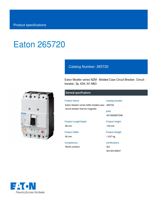
Eaton 265720Eaton Moeller series NZM - Molded Case Circuit Breaker. Circuit-breaker, 3p, 63A, N1-M63General specificationsEaton Moeller series NZM molded case circuit breaker thermo-magnetic265720401508265720888 mm 145 mm 90 mm 1.037 kg RoHS conformIEC IEC/EN 60947Product NameCatalog NumberEANProduct Length/Depth Product Height Product Width Product Weight Compliances Certifications63 AIs the panel builder's responsibility. The specifications for the switchgear must be observed.7.5 kA35 kAMeets the product standard's requirements.Is the panel builder's responsibility. The specifications for the switchgear must be observed.Built-in device fixed built-in techniqueFixed63 ADoes not apply, since the entire switchgear needs to be evaluated.Min. 2 segments of 9 mm x 0.8 mm at box terminalMax. 9 segments of 9 mm x 0.8 mm at box terminalRocker leverMeets the product standard's requirements.40 °CThermal protectionFinger and back-of-hand proof to VDE 0106 part 100eaton-digital-nzm-brochure-br013003en-en-us.pdfeaton-feerum-the-whole-grain-solution-success-story-en-us.pdfeaton-digital-nzm-catalog-ca013003en-en-us.pdfDA-DC-03_N1eaton-circuit-breaker-let-through-current-nzm-mccb-characteristic-curve-002.epseaton-circuit-breaker-nzm-mccb-characteristic-curve-058.epseaton-circuit-breaker-nzm-mccb-characteristic-curve.epseaton-circuit-breaker-nzm-mccb-dimensions-017.epseaton-circuit-breaker-switch-nzm-mccb-dimensions-014.epseaton-general-ie-ready-dilm-contactor-standards.epsMN1-M63eaton-circuit-breakers-nzm-pn1-nzmbc-nzmbn-circuit-breaker-switch-disconnector-instruction-leaflet-il01203004z.pdfIntroduction of the new digital circuit breaker NZMThe new digital NZM RangeDA-CS-nzm1_3pDA-CD-nzm1_3peaton-nzm-technical-information-sheeteaton-manual-motor-starters-starter-nzm-mccb-wiring-diagram.eps eaton-manual-motor-starters-starter-msc-r-reversing-starter-wiring-diagram.epsRated operational current for specified heat dissipation (In) 10.11 Short-circuit ratingRated short-circuit breaking capacity Ics (IEC/EN 60947) at 690 V, 50/60 HzRated short-circuit breaking capacity Icu (IEC/EN 60947) at 400/415 V, 50/60 Hz10.4 Clearances and creepage distances10.12 Electromagnetic compatibilityMounting MethodAmperage Rating10.2.5 LiftingTerminal capacity (copper strip)Handle type10.2.3.1 Verification of thermal stability of enclosuresAmbient storage temperature - minFitted with:Protection against direct contact BrochuresCatalogs Certification reports Characteristic curveDrawingseCAD model Installation instructions Installation videos mCAD model Technical data sheets Wiring diagramsTerminal capacity (copper busbar)Max. 16 mm x 5 mm direct at switch rear-side connection M6 at rear-side screw connectionMin. 12 mm x 5 mm direct at switch rear-side connection10.8 Connections for external conductorsIs the panel builder's responsibility.Special featuresMaximum back-up fuse, ifthe expected short-circuitcurrents at the installationlocation exceed theswitching capacity of thecircuit breaker (Rated short-circuit breaking capacity Icn)Rated current = rateduninterrupted current: 63 ATerminal capacity hint: Up to95 mm² can be connecteddepending on the cablemanufacturer.With phase-failure sensitivityTripping class 10 AIEC/EN 60947-4-1, IEC/EN60947-2The circuit-breaker fulfills allrequirements for AC-3switching category.Ambient operating temperature - max70 °CClimatic proofingDamp heat, constant, to IEC 60068-2-78Damp heat, cyclic, to IEC 60068-2-30Terminal capacity (aluminum stranded conductor/cable)25 mm² - 35 mm² (2x) direct at switch rear-side connection 25 mm² - 35 mm² (1x) direct at switch rear-side connection 25 mm² - 95 mm² (1x) at tunnel terminalTerminal capacity (copper stranded conductor/cable)10 mm² - 70 mm² (1x) direct at switch rear-side connection 10 mm² - 70 mm² (1x) at box terminal6 mm² - 25 mm² (2x) at box terminal25 mm² - 95 mm² (1x) at 1-hole tunnel terminal25 mm² (2x) direct at switch rear-side connection Lifespan, electrical7500 operations at 690 V AC-110000 operations at 415 V AC-15000 operations at 690 V AC-37500 operations at 400 V AC-310000 operations at 400 V AC-17500 operations at 415 V AC-3Electrical connection type of main circuitOtherShort-circuit total breaktime< 10 msRated impulse withstand voltage (Uimp) at main contacts6000 VRated short-circuit breaking capacity Ics (IEC/EN 60947) at 400/415 V, 50/60 Hz35 kA10.9.3 Impulse withstand voltageIs the panel builder's responsibility.Utilization categoryA (IEC/EN 60947-2)Number of polesThree-poleAmbient operating temperature - min-25 °C10.6 Incorporation of switching devices and componentsDoes not apply, since the entire switchgear needs to be evaluated.10.5 Protection against electric shockDoes not apply, since the entire switchgear needs to be evaluated.Terminal capacity (control cable)0.75 mm² - 2.5 mm² (1x)0.75 mm² - 1.5 mm² (2x)Equipment heat dissipation, current-dependent14.88 WInstantaneous current setting (Ii) - min504 A10.13 Mechanical functionThe device meets the requirements, provided the information in the instruction leaflet (IL) is observed.10.2.6 Mechanical impactDoes not apply, since the entire switchgear needs to be evaluated.10.9.4 Testing of enclosures made of insulating materialIs the panel builder's responsibility.Rated operational current55 A (400 V AC-3)Rated short-circuit breaking capacity Ics (IEC/EN 60947) at 230 V, 50/60 Hz85 kAApplicationUse in unearthed supply systems at 690 V10.3 Degree of protection of assembliesDoes not apply, since the entire switchgear needs to be evaluated.Rated short-circuit making capacity Icm at 240 V, 50/60 Hz187 kARated short-circuit breaking capacity Ics (IEC/EN 60947) at 440 V, 50/60 Hz35 kADegree of protection (IP), front sideIP66 (with door coupling rotary handle)IP40 (with insulating surround)Rated short-circuit making capacity Icm at 525 V, 50/60 Hz40 kARated short-circuit making capacity Icm at 690 V, 50/60 Hz17 kAInstantaneous current setting (Ii) - max882 AOverload current setting (Ir) - min50 A10.2.3.2 Verification of resistance of insulating materials to normal heatMeets the product standard's requirements.10.2.3.3 Resist. of insul. mat. to abnormal heat/fire by internal elect. effectsMeets the product standard's requirements.Lifespan, mechanical20000 operationsOverload current setting (Ir) - max63 AVoltage rating690 V - 690 VTerminal capacity (copper solid conductor/cable)6 mm² - 16 mm² (2x) direct at switch rear-side connection16 mm² (1x) at tunnel terminal6 mm² - 16 mm² (2x) at box terminal10 mm² - 16 mm² (1x) at box terminal10 mm² - 16 mm² (1x) direct at switch rear-side connectionDegree of protection (terminations)IP10 (tunnel terminal)IP00 (terminations, phase isolator and strip terminal)10.9.2 Power-frequency electric strengthIs the panel builder's responsibility.Short-circuit release non-delayed setting - min504 ADegree of protectionIP20 (basic degree of protection, in the operating controls area) IP20Overvoltage categoryIIIRated impulse withstand voltage (Uimp) at auxiliary contacts 6000 VTerminal capacity (aluminum solid conductor/cable)10 mm² - 16 mm² (2x) direct at switch rear-side connection10 mm² - 16 mm² (1x) direct at switch rear-side connection16 mm² (1x) at tunnel terminalSwitch off techniqueThermomagneticAmbient storage temperature - max70 °CRated short-circuit breaking capacity Ics (IEC/EN 60947) at 525 V, 50/60 Hz10 kAOptional terminalsConnection on rear. Screw terminal. Tunnel terminalRelease systemThermomagnetic releasePollution degree310.7 Internal electrical circuits and connectionsIs the panel builder's responsibility.Rated operating power at AC-3, 230 V18.5 kW10.10 Temperature riseThe panel builder is responsible for the temperature rise calculation. Eaton will provide heat dissipation data for the devices.FunctionsPhase failure sensitiveMotor protectionShort-circuit release non-delayed setting - max882 AStandard terminalsBox terminalRated short-circuit making capacity Icm at 400/415 V, 50/60 Hz 105 kARated operating power at AC-3, 400 V30 kWTypeCircuit breaker10.2.2 Corrosion resistanceMeets the product standard's requirements.10.2.4 Resistance to ultra-violet (UV) radiationMeets the product standard's requirements.10.2.7 InscriptionsMeets the product standard's requirements.Rated short-circuit making capacity Icm at 440 V, 50/60 Hz74 kAIsolation300 V AC (between the auxiliary contacts)500 V AC (between auxiliary contacts and main contacts)Number of operations per hour - max120Circuit breaker frame typeNZM1Eaton Corporation plc Eaton House30 Pembroke Road Dublin 4, Ireland © 2023 Eaton. All Rights Reserved. Eaton is a registered trademark.All other trademarks areproperty of their respectiveowners./socialmediaAs required 20 g (half-sinusoidal shock 20 ms)690 VDirection of incoming supply Shock resistanceRated insulation voltage (Ui)。
MAX706中文资料_数据手册_参数

UNREGULATED DC
MAX667 +5V DC LINEAR
REGULATOR
PUSHBUTTON SWITCH
VCC
RESMR
MAX706 MAX813L
PFO
µP
VCC RESET I/O LINE NMI INTERRUPT
___________________________Features
o Available in Tiny µMAX Package
o Guaranteed RESET Valid at VCC = 1V o Precision Supply-Voltage Monitor
4.65V in MAX705/MAX707/MAX813L 4.40V in MAX706/MAX708
Output Current (all outputs) . . . . . . . . . . . . . . . . . . . . . . . . . . . . . 20mA Continuous Power Dissipation (TA = +70°C)
Plastic DIP (derate 9.09mW/°C above +70°C) . . . . . . . 727mW SO (derate 5.88mW/°C above +70°C) . . . . . . . . . . . . . . . 471mW µMAX (derate 4.10mW/°C above +70°C) . . . . . . . . . . . . 330mW
3) A 1.25V threshold detector for power-fail warning, low-battery detection, or for monitoring a power supply other than +5V.
绿色Max数字开关说明书

Leviton Manufacturing Co., Inc. Lighting & Controls20497 SW Teton Avenue, Tualatin, OR 97062 tech line 800-959-6004 fax 503-404-5594© 2020 Leviton Manufacturing Co., Inc. All rights reserved. Subject to change without notice.G r e e n M A X ®D i g i t a l S w i t c h e sGreenMAX® Digital Switches Offers Programming FlexibilityLeviton GreenMAX® Digital Switches are 100% digital. Specifically designed for use with GreenMAX Relay Control Panels, GreenMAX Digital Switches utilize LumaCAN protocolsfor unparalleled programming flexibility. All communication and monitoring functionscan be performed from any GreenMAX Digital Switch location. Simply connect the GreenMAX Handheld Display Unit (HDU) to any GreenMAX Digital Switch for easy programming and system control of all devices on the GreenMAX network. Available in 1-, 2-, 4-, 8-button and keyswitch configurations, these switches connect using RJ45 connectors and CAT6 cabling. For dimming applications, use 4-button switch with dimming module for control of0-10V dimming circuits.APPLICATIONS• Heavy retrofit applications• New construction projects• Government facilities• Office buildings• Hospitals/medical offices• Universities• Restaurants• Large campuses• Any other location where centralized lighting control, programming and monitoring are requiredFEATURES• Models include 1-, 2-, 4-, 8-button and keyswitch configurations• RJ45 connectors to provide IN and OUT connections to the LumaCAN network• Complies with energy code requirements for Title 24 2013 when used with GreenMAX Relay Systems • Any button can be configured to control0-10VDC dimming circuits• Easy-to-access port on top of switch provides connectivity for the GreenMAX HDU• Custom engraved labeling available on switch buttons and screwless wall plates- 1, 2, 4 button: up to 8 characters per two lines of text*- 8 button: up to 4 characters per one line of text*• Install a mix of GreenMAX Relay Panels, Remote Input Cabinets and Digital Switches on a single LumaCAN• Buttons can be programmed for ON, OFF, ON/OFF, dimmed raise/lower or single zone preset ON level• Status LED for each button provides true relay status• Matching screwless single-gang wall plate is supplied and digital switches are compatible with all available Decora® wall plates*• Mounts in a standard depth wall box. All switches can be installed in a multi-gang application. The multi-gang wall plate is sold separately.• Use with GreenMAX Relay Systems• Available in White, Ivory, Light Almond and Gray. Color change kit available for Black and Red buttons (key switch stainless only).• Draws its power from the LumaCAN• Keyswitch includes a set of 2 keys, stainless steel wall plate, tamper resistant screws and installation tool*• Keyswitch is spring return to the center position. Quarter turn of the key functionsas a momentary switch input. Key can be removed in the center position only.*Excluding keyswitchGreenMAX Key SwitchGreenMAX Digital SwitchesPRODUCT DATASPECIFICATIONSElectrical• Input Power: 24VDC (LumaCAN integral)• Consumption: 1 Unit Load = 25mA (max)• Connectors: RJ45• Class 2• Cables: Cat6Environmental• Ambient Temperature Range: 32 - 122°F (0 - 50°C)• Relative Humidity: <90% non-condensingListings• Complies with energy code requirements for ASHRAE Standard 90.1 2010 and Title 24 2013 Warranty• Limited 2-Year WarrantyDIMENSIONS1,2,4,8 Button SwitchesKeyswitch A 1.65” (42.06mm) 1.70” (43.18mm)B4.60” (117.07mm) 4.50” (114.30mm)C 2.75” (69.85mm) 2.75” (69.85mm)D 0.37” (9.55mm)0.28” (7.21mm)E1.16” (29.51mm) 1.88” (47.88mm)F2.68” (68.25mm)2.70” (68.58mm)WIRING DIAGRAM * Replace x to indicate color: (W) = White, (I) = Ivory, (T) = Light Almond, (G) = GrayReplace y to indicate color: (W) = White, (I) = Ivory, (T) = Light Almond, (G) = Gray (R) = Red, (E) = Black ** Stainless steel wallplate cannot be engraved. Multi-gang keyswitch order requires a custom wallplateG-8320F/L19-AJAREV DEC 2019Leviton Manufacturing Co., Inc. Lighting & Controls20497 SW Teton Avenue, Tualatin, OR 97062 tel 800-736-6682 fax 503-404-5594 tech line (6:00AM-4:00PM PT Mon-Fri) 800-959-6004Leviton Manufacturing Co., Inc. Global Headquarters201 North Service Road, Melville, NY 11747-3138 tel 800-323-8920 fax 800-832-9538 tech line (8:30AM-7:00PM ET Mon-Fri) 800-824-3005Visit our Website at: /greenmax©2020 Leviton Manufacturing Co., Inc. All rights reserved. Subject to change without notice.。
MAX6316LUK48DW-T中文资料

___________________________________________________________________Selector Guide________________General DescriptionThe MAX6316–MAX6322 family of microprocessor (µP)supervisory circuits monitors power supplies and microprocessor activity in digital systems. It offers sev-eral combinations of push/pull, open-drain, and bidirec-tional (such as Motorola 68HC11) reset outputs, along with watchdog and manual reset features. The Selector Guide below lists the specific functions available from each device. These devices are specifically designed to ignore fast negative transients on V CC . Resets are guaranteed valid for V CC down to 1V.These devices are available in 26 factory-trimmed reset threshold voltages (from 2.5V to 5V, in 100mV incre-ments), featuring four minimum power-on reset timeout periods (from 1ms to 1.12s), and four watchdog timeout periods (from 6.3ms to 25.6s). Thirteen standard ver-sions are available with an order increment requirement of 2500 pieces (see Standard Versions table); contact the factory for availability of other versions, which have an order increment requirement of 10,000 pieces.The MAX6316–MAX6322 are offered in a miniature 5-pin SOT23 package.________________________ApplicationsPortable Computers Computers ControllersIntelligent InstrumentsPortable/Battery-Powered Equipment Embedded Control Systems____________________________Features♦Small 5-Pin SOT23 Package♦Available in 26 Reset Threshold Voltages2.5V to 5V, in 100mV Increments ♦Four Reset Timeout Periods1ms, 20ms, 140ms, or 1.12s (min)♦Four Watchdog Timeout Periods6.3ms, 102ms, 1.6s, or 25.6s (typ) ♦Four Reset Output StagesActive-High, Push/Pull Active-Low, Push/Pull Active-Low, Open-Drain Active-Low, Bidirectional♦Guaranteed Reset Valid to V CC = 1V♦Immune to Short Negative V CC Transients ♦Low Cost♦No External ComponentsMAX6316–MAX63225-Pin µP Supervisory Circuits withWatchdog and Manual Reset________________________________________________________________Maxim Integrated Products 119-0496; Rev 7; 11/07_______________Ordering InformationOrdering Information continued at end of data sheet.*The MAX6318/MAX6319/MAX6321/MAX6322 feature two types of reset output on each device.Typical Operating Circuit and Pin Configurations appear at end of data sheet.For pricing, delivery, and ordering information, please contact Maxim Direct at 1-888-629-4642,or visit Maxim’s website at .Specify lead-free by replacing “-T” with “+T” when ordering.ELECTRICAL CHARACTERISTICS(V CC = 2.5V to 5.5V, T A = -40°C to +125°C, unless otherwise noted. Typical values are at T A = +25°C.) (Note 1)M A X 6316–M A X 63225-Pin µP Supervisory Circuits with Watchdog and Manual Reset 2_______________________________________________________________________________________ABSOLUTE MAXIMUM RATINGSStresses beyond those listed under “Absolute Maximum Ratings” may cause permanent damage to the device. These are stress ratings only, and functional operation of the device at these or any other conditions beyond those indicated in the operational sections of the specifications is not implied. Exposure to absolute maximum rating conditions for extended periods may affect device reliability.Voltage (with respect to GND)V CC ......................................................................-0.3V to +6V RESET (MAX6320/MAX6321/MAX6322 only)...... -0.3V to +6V All Other Pins.........................................-0.3V to (V CC + 0.3V)Input/Output Current, All Pins.............................................20mAContinuous Power Dissipation (T A = +70°C)SOT23-5 (derate 7.1mW/°C above +70°C)...............571mW Operating Temperature Range..........................-40°C to +125°C Junction Temperature......................................................+150°C Storage Temperature Range..............................-65°C to +160°C Lead Temperature (soldering, 10s).................................+300°CTH available in 100mV increments from 2.5V to 5V (see Table 1 at end of data sheet).Note 3:Guaranteed by design.MAX6316–MAX63225-Pin µP Supervisory Circuits withWatchdog and Manual Reset_______________________________________________________________________________________3Note 5:Measured from RESET V OL to (0.8 x V CC ), R LOAD = ∞.Note 6:WDI is internally serviced within the watchdog period if WDI is left unconnected.Note 7:The WDI input current is specified as the average input current when the WDI input is driven high or low. The WDI input is designed for a three-stated-output device with a 10µA maximum leakage current and capable of driving a maximum capac-itive load of 200pF. The three-state device must be able to source and sink at least 200µA when active.ELECTRICAL CHARACTERISTICS (continued)M A X 6316–M A X 63225-Pin µP Supervisory Circuits with Watchdog and Manual Reset 4_________________________________________________________________________________________________________________________________Typical Operating Characteristics(T A = +25°C, unless otherwise noted.)021*********-4020-20406080100MAX6316/MAX6317/MAX6318/MAX6320/MAX6321SUPPLY CURRENT vs. TEMPERATURETEMPERATURE (°C)S U P P L Y C U R R E N T (μA )302010504090807060100-40-20020406080100V CC FALLING TO RESET PROPAGATIONDELAY vs. TEMPERATURETEMPERATURE (°C)R E S E T P R O P A G A T I O N D E L A Y (μs )140180160240220200300280260320-40020-20406080100MAX6316/MAX6317/MAX6319/MAX6320/MAX6322MANUAL RESET TO RESETPROPAGATION DELAY vs. TEMPERATURETEMPERATURE (°C)P R O P A G A T I O N D E L A Y (n s )0.950.980.970.961.000.991.041.031.021.011.05-40-2020406080100NORMALIZED RESET TIMEOUT PERIOD vs. TEMPERATUREM A X 6316t o c 04TEMPERATURE (°C)N O R M A L I Z E D R E S E T T I M E O U T P E R I O D0.950.980.970.961.000.991.041.031.021.011.05-40-2020406080100MAX6316/MAX6317/MAX6318/MAX6320/MAX6321NORMALIZED WATCHDOG TIMEOUTPERIOD vs. TEMPERATUREM A X 6316t o c 05TEMPERATURE (°C)N O R M A L I Z E D W A T C H D O G T I M E O U T P E R I O D800101001000MAXIMUM V CC TRANSIENT DURATION vs. RESET THRESHOLD OVERDRIVE2010RESET THRESHOLD OVERDRIVE (mV) V RST - V CCT RA N S I E N T D U R A T I O N (μs )3050604070200ns/divMAX6316M/6318MH/6319MHBIDIRECTIONALPULLUP CHARACTERISTICSMAX6316–MAX63225-Pin µP Supervisory Circuits withWatchdog and Manual Reset_______________________________________________________________________________________5______________________________________________________________Pin DescriptionM A X 6316–M A X 63225-Pin µP Supervisory Circuits with Watchdog and Manual Reset 6______________________________________________________________________________________________________Detailed DescriptionA microprocessor’s (µP) reset input starts or restarts the µP in a known state. The reset output of the MAX6316–MAX6322 µP supervisory circuits interfaces with the reset input of the µP, preventing code-execution errors during power-up, power-down, and brownout condi-tions (see the Typical Operating Circuit ). The MAX6316/MAX6317/MAX6318/MAX6320/MAX6321 are also capa-ble of asserting a reset should the µP become stuck in an infinite loop.Reset OutputThe MAX6316L/MAX6318LH/MAX6319LH feature an active-low reset output, while the MAX6317H/MAX6318_H/MAX6319_H/MAX6321HP/MAX6322HP feature an active-high reset output. RESET is guaran-teed to be a logic low and RESET is guaranteed to be a logic high for V CC down to 1V.The MAX6316–MAX6322 assert reset when V CC is below the reset threshold (V RST ), when MR is pulled low (MAX6316_/MAX6317H/MAX6319_H/MAX6320P/MAX6322HP only), or if the WDI pin is not serviced withinthe watchdog timeout period (t WD ). Reset remains assert-ed for the specified reset active timeout period (t RP ) after V CC rises above the reset threshold, after MR transitions low to high, or after the watchdog timer asserts the reset (MAX6316_/MAX6317H/MAX6318_H/MAX6320P/MAX6321HP). After the reset active timeout period (t RP )expires, the reset output deasserts, and the watchdog timer restarts from zero (Figure 2).Figure 1. Functional DiagramFigure 2. Reset Timing DiagramMAX6316–MAX63225-Pin µP Supervisory Circuits withWatchdog and Manual Reset_______________________________________________________________________________________7Bidirectional R E S E T OutputThe MAX6316M/MAX6318MH/MAX6319MH are designed to interface with µPs that have bidirectional reset pins,such as the Motorola 68HC11. Like an open-drain output,these devices allow the µP or other devices to pull the bidirectional reset (RESET ) low and assert a reset condi-tion. However, unlike a standard open-drain output, it includes the commonly specified 4.7k Ωpullup resistor with a P-channel active pullup in parallel.This configuration allows the MAX6316M/MAX6318MH/MAX6319MH to solve a problem associated with µPs that have bidirectional reset pins in systems where sev-eral devices connect to RESET (F igure 3). These µPs can often determine if a reset was asserted by an exter-nal device (i.e., the supervisor IC) or by the µP itself (due to a watchdog fault, clock error, or other source),and then jump to a vector appropriate for the source of the reset. However, if the µP does assert reset, it does not retain the information, but must determine the cause after the reset has occurred.The following procedure describes how this is done in the Motorola 68HC11. In all cases of reset, the µP pulls RESET low for about four external-clock cycles. It then releases RESET , waits for two external-clock cycles,then checks RESET ’s state. If RESET is still low, the µP concludes that the source of the reset was external and, when RESET eventually reaches the high state, it jumps to the normal reset vector. In this case, stored-state information is erased and processing begins fromscratch. If, on the other hand, RESET is high after a delay of two external-clock cycles, the processor knows that it caused the reset itself and can jump to a different vector and use stored-state information to determine what caused the reset.A problem occurs with faster µPs; two external-clock cycles are only 500ns at 4MHz. When there are several devices on the reset line, and only a passive pullup resis-tor is used, the input capacitance and stray capacitance can prevent RESET from reaching the logic high state (0.8✕V CC ) in the time allowed. If this happens, all resets will be interpreted as external. The µP output stage is guaran-teed to sink 1.6mA, so the rise time can not be reduced considerably by decreasing the 4.7k Ωinternal pullup resistance. See Bidirectional Pullup Characteristics in the Typical Operating Characteristics .The MAX6316M/MAX6318MH/MAX6319MH overcome this problem with an active pullup FET in parallel with the 4.7k Ωresistor (F igures 4 and 5). The pullup transistor holds RESET high until the µP reset I/O or the supervisory circuit itself forces the line low. Once RESET goes below V PTH , a comparator sets the transition edge flip-flop, indi-cating that the next transition for RESET will be low to high. When RESET is released, the 4.7k Ωresistor pulls RESET up toward V CC . Once RESET rises above V PTH but is below (0.85 x V CC ), the active P-channel pullup turns on. Once RESET rises above (0.85 x V CC ) or the 2µs one-shot times out, the active pullup turns off. The parallel combination of the 4.7k Ωpullup and theFigure 3. MAX6316M/MAX6318MH/MAX6319MH Supports Additional Devices on the Reset BusM A X 6316–M A X 63225-Pin µP Supervisory Circuits with Watchdog and Manual Reset 8_______________________________________________________________________________________Figure 4. MAX6316/MAX6318MH/MAX6319MH Bidirectional Reset Output Functional DiagramMAX6316–MAX63225-Pin µP Supervisory Circuits withWatchdog and Manual Reset_______________________________________________________________________________________9P-channel transistor on-resistance quickly charges stray capacitance on the reset line, allowing RESET to transition from low to high within the required two elec-tronic-clock cycles, even with several devices on the reset line. This process occurs regardless of whether the reset was caused by V CC dipping below the reset threshold, the watchdog timing out, MR being asserted,or the µP or other device asserting RESET . The parts do not require an external pullup. To minimize supply cur-rent consumption, the internal 4.7k Ωpullup resistor dis-connects from the supply whenever the MAX6316M/MAX6318MH/MAX6319MH assert reset.Open-Drain R E S E T OutputThe MAX6320P/MAX6321HP/MAX6322HP have an active-low, open-drain reset output. This output struc-ture will sink current when RESET is asserted. Connect a pullup resistor from RESET to any supply voltage up to 6V (Figure 6). Select a resistor value large enough toregister a logic low (see Electrical Characteristics ), and small enough to register a logic high while supplying all input current and leakage paths connected to the RESET line. A 10k Ωpullup is sufficient in most applications.Manual-Reset InputThe MAX6316_/MAX6317H/MAX6319_H/MAX6320P/MAX6322HP feature a manual reset input. A logic low on MR asserts a reset. After MR transitions low to high, reset remains asserted for the duration of the reset timeout peri-od (t RP ). The MR input is connected to V CC through an internal 52k Ωpullup resistor and therefore can be left unconnected when not in use. MR can be driven with TTL-logic levels in 5V systems, with CMOS-logic levels in 3V systems, or with open-drain or open-collector output devices. A normally-open momentary switch from MR to ground can also be used; it requires no external debouncing circuitry. MR is designed to reject fast, negative-going transients (typically 100ns pulses). A 0.1µF capacitor from MR to ground provides additional noise immunity.The MR input pin is equipped with internal ESD-protection circuitry that may become forward biased. Should MR be driven by voltages higher than V CC , excessive current would be drawn, which would damage the part. F or example, assume that MR is driven by a +5V supply other than V CC . If V CC drops lower than +4.7V, MR ’s absolute maximum rating is violated [-0.3V to (V CC + 0.3V)], and undesirable current flows through the ESD structure from MR to V CC . To avoid this, use the same supply for MR as the supply monitored by V CC . This guarantees that the voltage at MR will never exceed V CC .Watchdog InputThe MAX6316_/MAX6317H/MAX6318_H/MAX6320P/MAX6321HP feature a watchdog circuit that monitors the µP’s activity. If the µP does not toggle the watchdog input (WDI) within the watchdog timeout period (t WD ),reset asserts. The internal watchdog timer is cleared by reset or by a transition at WDI (which can detect pulses as short as 50ns). The watchdog timer remains cleared while reset is asserted. Once reset is released, the timer begins counting again (Figure 7).The WDI input is designed for a three-stated output device with a 10µA maximum leakage current and the capability of driving a maximum capacitive load of 200pF.The three-state device must be able to source and sink at least 200µA when active. Disable the watchdog function by leaving WDI unconnected or by three-stating the driver connected to WDI. When the watchdog timer is left open circuited, the timer is cleared internally at intervals equal to 7/8 of the watchdog period.Figure 6. MAX6320P/MAX6321HP/MAX6322HP Open-Drain RESET Output Allows Use with Multiple SuppliesFigure 5. Bidirectional RESET Timing DiagramM A X 6316–M A X 63225-Pin µP Supervisory Circuits with Watchdog and Manual Reset 10______________________________________________________________________________________Applications InformationWatchdog Input CurrentThe WDI input is internally driven through a buffer and series resistor from the watchdog counter. For minimum watchdog input current (minimum overall power con-sumption), leave WDI low for the majority of the watch-dog timeout period. When high, WDI can draw as much as 160µA. Pulsing WDI high at a low duty cycle will reduce the effect of the large input current. When WDI is left unconnected, the watchdog timer is serviced within the watchdog timeout period by a low-high-low pulse from the counter chain.Negative-Going V CC TransientsThese supervisors are immune to short-duration, nega-tive-going V CC transients (glitches), which usually do not require the entire system to shut down. Typically,200ns large-amplitude pulses (from ground to V CC ) on the supply will not cause a reset. Lower amplitude puls-es result in greater immunity. Typically, a V CC transient that goes 100mV under the reset threshold and lasts less than 4µs will not trigger a reset. An optional 0.1µF bypass capacitor mounted close to V CC provides addi-tional transient immunity.Ensuring Valid Reset OutputsDown to V CC = 0The MAX6316_/MAX6317H/MAX6318_H/MAX6319_H/MAX6321HP/MAX6322HP are guaranteed to operate properly down to V CC = 1V. In applications that require valid reset levels down to V CC = 0, a pulldown resistor to active-low outputs (push/pull and bidirectional only,F igure 8) and a pullup resistor to active-high outputs(push/pull only, Figure 9) will ensure that the reset line is valid while the reset output can no longer sink orsource current. This scheme does not work with the open-drain outputs of the MAX6320/MAX6321/MAX6322.The resistor value used is not critical, but it must be large enough not to load the reset output when V CC is above the reset threshold. F or most applications,100k Ωis adequate.Watchdog Software Considerations(MAX6316/MAX6317/MAX6318/MAX6320/MAX6321)One way to help the watchdog timer monitor software execution more closely is to set and reset the watchdog input at different points in the program, rather than pulsing the watchdog input high-low-high or low-high-low. This technique avoids a stuck loop, in which the watchdog timer would continue to be reset inside the loop, keeping the watchdog from timing out.Figure 7. Watchdog Timing RelationshipFigure 9. Ensuring RESET Valid to V CC = 0 on Active-High Push/Pull OutputsFigure 8. Ensuring RESET Valid to V CC = 0 on Active-Low Push/Pull and Bidirectional OutputsMAX6316–MAX6322Watchdog and Manual Reset______________________________________________________________________________________11F igure 10 shows an example of a flow diagram where the I/O driving the watchdog input is set high at the beginning of the program, set low at the end of every subroutine or loop, then set high again when the pro-gram returns to the beginning. If the program should hang in any subroutine, the problem would be quickly corrected, since the I/O is continually set low and the watchdog timer is allowed to time out, causing a reset or interrupt to be issued. As described in the Watchdog Input Current section, this scheme results in higher time average WDI current than does leaving WDI low for the majority of the timeout period and periodically pulsing it low-high-low.Figure 10. Watchdog Flow Diagram__________________Pin ConfigurationsTypical Operating CircuitTable 2. Standard VersionsTable 1. Factory-Trimmed Reset ThresholdsM A X 6316–M A X 6322Watchdog and Manual ResetTable 3. Reset/Watchdog Timeout PeriodsMAX6316–MAX6322Watchdog and Manual Reset______________________________________________________________________________________13__Ordering Information (continued)a watchdog feature (see Selector Guide) are factory-trimmed to one of four watchdog timeout periods. Insert the letter corre-sponding to the desired watchdog timeout period (W, X, Y, or Z from Table 3) into the blank following the reset timeout suffix.TRANSISTOR COUNT: 191SUBSTRATE IS INTERNALLY CONNECTED TO V+Chip Informationdard versions only. The required order increment for nonstandard versions is 10,000 pieces. Contact factory for availability.M A X 6316–M A X 6322Watchdog and Manual Reset 14______________________________________________________________________________________Package Information(The package drawing(s) in this data sheet may not reflect the most current specifications. For the latest package outline information,go to /packages .)M axim cannot assume responsibility for use of any circuitry other than circuitry entirely embodied in a M axim product. No circuit patent licenses are implied. Maxim reserves the right to change the circuitry and specifications without notice at any time.Maxim Integrated Products, 120 San Gabriel Drive, Sunnyvale, CA 94086 408-737-7600 ____________________15©2007 Maxim Integrated Productsis a registered trademark of Maxim Integrated Products, Inc.MAX6316–MAX6322 Watchdog and Manual ResetRevision History。
MAX6356RVUT中文资料

For pricing, delivery, and ordering information, please contact Maxim/Dallas Direct! at 1-888-629-4642, or visit Maxim’s website at .
元器件交易网
Dual/Triple-Voltage µP Supervisory Circuits MAX6351–MAX6360
ABSOLUTE MAXIMUM RATINGS
VCC1, VCC2 to GND .................................................-0.3V to +6V RST (MAX6352/MAX6355/MAX6358)...................... -0.3V to +6V RST, MR, WDI, RST1, RSTIN (MAX6351/MAX6353/ MAX6356/MAX6359) ..............................-0.3V to (VCC1 + 0.3V) RST, RST2 (MAX6351/MAX6354/ MAX6357/MAX6360) ..............................-0.3V to (VCC2 + 0.3V) Input/Output Current, All Pins .............................................20mA Continuous Power Dissipation (TA = +70°C) 5-Pin SOT23 (derate 7.1mW/°C above +70°C)............571mW 6-Pin SOT23 (derate 8.7mW/°C above +70°C)............695mW Operating Temperature Range ...........................-40°C to +85°C Junction Temperature .....................................................+150°C Storage Temperature Range .............................-65°C to +150°C
MAX6305中文资料
For free samples & the latest literature: , or phone 1-800-998-8800.For small orders, phone 408-737-7600 ext. 3468.General DescriptionThe MAX6305–MAX6313 CMOS microprocessor (µP)supervisory circuits are designed to monitor more than one power supply. Ideal for monitoring both 5V and 3.3V in personal computer systems, these devicesFeatureso Small 5-Pin SOT23 Packageo Precision Factory-Set V CC Reset Thresholds;Available in 0.1V Increments from 2.5V to 5V o Immune to Short V TransientsMAX6305–MAX63135-Pin, Multiple-Input,Programmable Reset ICs________________________________________________________________Maxim Integrated Products 119-1145; Rev 1; 8/98M A X 6305–M A X 63135-Pin, Multiple-Input, Programmable Reset ICs 2_______________________________________________________________________________________ABSOLUTE MAXIMUM RATINGSELECTRICAL CHARACTERISTICSV CC = +2.5V to +5.5V for the MAX6305/MAX6308/MAX6311, V CC = (V TH + 2.5%) to +5.5V for the MAX6306/MAX6307/MAX6309/MAX6310/MAX6312/MAX6313; T A = 0°C to +70°C; unless otherwise noted. Typical values are at T A = +25°C.)Stresses beyond those listed under “Absolute Maximum Ratings” may cause permanent damage to the device. These are stress ratings only, and functional operation of the device at these or any other conditions beyond those indicated in the operational sections of the specifications is not implied. Exposure to absolute maximum rating conditions for extended periods may affect device reliability.V CC ...........................................................................-0.3V to +6V All Other Pins..............................................-0.3V to (V CC + 0.3V)Input/Output Current, All Pins.............................................20mA Rate of Rise, V CC ............................................................100V/µsContinuous Power Dissipation (T A = +70°C)SOT23-5 (derate 7.1mW/°C above +70°C).................571mW Operating Temperature Range...............................0°C to +70°C Storage Temperature Range.............................-65°C to +160°C Lead Temperature (soldering, 10sec).............................+300°CMAX6305–MAX63135-Pin, Multiple-Input, Programmable Reset ICs_______________________________________________________________________________________3ELECTRICAL CHARACTERISTICS (continued)(V CC = +2.5V to +5.5V for the MAX6305/MAX6308/MAX6311, V CC = (V TH + 2.5%) to +5.5V for the MAX6306/MAX6307/MAX6309/MAX6310/MAX6312/MAX6313; T A = 0°C to +70°C; unless otherwise noted. Typical values are at T A = +25°C.)Note 1: The MAX6305/MAX6308/MAX6311 switch from undervoltage reset to normal operation between 1.5V < V CC < 2.5V.Note 2: The MAX6306/MAX6307/MAX6309/MAX6310/MAX6312/MAX6313 monitor V CC through an internal factory-trimmed voltagedivider, which programs the nominal reset threshold. Factory-trimmed reset thresholds are available in approximately 100mV increments from 2.5V to 5V (Table 1).M A X 6305–M A X 63135-Pin, Multiple-Input, Programmable Reset ICs 4_________________________________________________________________________________________________________________________________Typical Operating Characteristics(V CC = +5V, T A = +25°C, unless otherwise noted.)5.05.56.06.57.07.58.08.59.09.5-60-40-2020406080100SUPPLY CURRENT vs. TEMPERATURETEMPERATURE (°C)S U P P L Y C U R R E N T (µA )01020304050607080-60-40-2020406080100V CC FALLING PROPAGATION DELAYvs. TEMPERATURETEMPERATURE (°C)P R O P A G A T I O N D E L A Y (n s )010203040506070-60-40-20020406080100OVRST IN RISING PROPAGATION DELAY vs. TEMPERATURE (OVERVOLTAGE RESET INPUT)TEMPERATURE (°C)P R O P A G A T I O N D E L A Y (n s )020406080100120-60-40-2020406080100RST IN_ FALLING PROPAGATION DELAY vs. TEMPERATURETEMPERATURE (°C)R S T I N _ P R O P A G A T I O N D E L A Y (n s )104001200800MAXIMUM TRANSIENT DURATION vs.V CC RESET THRESHOLD OVERDRIVE10OVERDRIVE, V TH - V CC (mV)T R A N S I E N T D U R A T I O N (µs )100100010,0000.900.920.940.960.981.001.021.041.061.081.10-60-40-20020406080100RESET TIMEOUT vs. TEMPERATURE6305 T O C 05TEMPERATURE (°C)N O R M A L I Z E D R E S E T T I M E O U T0.9900.9920.9940.9960.9981.0001.0021.0041.0061.0081.010-60-40-2020406080100RESET THRESHOLD vs. TEMPERATURE6305 T O C 06TEMPERATURE (°C)N O R M A L I Z E D R E S E T T H R E S H O L D (V /V )104001200800MAXIMUM TRANSIENT DURATION vs.OVRST IN THRESHOLD OVERDRIVE10OVERDRIVE, V OVRST IN - V REF (mV)T R A N S I E N T D U R A T I O N (µs )100100010,000104001200800MAXIMUM TRANSIENT DURATION vs.RST IN_ THRESHOLD OVERDRIVE10OVERDRIVE, V REF - V RST IN (mV)T R A N S I E N T D U R A T I O N (µs )100100010,000_______________Detailed DescriptionThe MAX6305–MAX6313 CMOS microprocessor (µP)supervisory circuits are designed to monitor more than one power supply and issue a system reset when any monitored supply falls out of regulation. The MAX6305/MAX6308/MAX6311 have two adjustable undervoltage reset inputs (RST IN1 and RST IN2). The MAX6306/MAX6307/MAX6309/MAX6310/MAX6312/MAX6313 mon-itor V CC through an internal, factory-trimmed voltage divider. The MAX6306/MAX6309/MAX6312 have, in addition, an adjustable undervoltage reset input and a manual-reset input. The internal voltage divider sets the reset threshold as specified in the device part number (Table 1). The MAX6307/MAX6310/ MAX6313 feature an adjustable undervoltage reset input (RST IN) and an adjustable overvoltage reset input (OVRST IN) in addition to the factory-trimmed reset threshold on the V CC moni-tor. Program the adjustable reset inputs with an external resistor divider (see Adjustable Reset Inputs section).Reset OutputsA µP’s reset input starts the µP in a known state. These µP supervisory circuits assert reset to prevent code-execution errors during power-up, power-down, or brownout conditions.RESET (MAX6305–MAX6310) and RESET (MAX6311/MAX6312/MAX6313) are guaranteed to be asserted at a valid logic level for V CC > 1V (see Electrical Characteristics ). Once all monitored voltages exceed their programmed reset thresholds, an internal timer keeps reset asserted for the reset timeout period (t RP );after this interval, reset deasserts.If a brownout condition occurs (any or all monitored volt-ages dip outside their programmed reset threshold),reset asserts (RESET goes high; RESET goes low). Any time any of the monitored voltages dip below their reset threshold, the internal timer resets to zero and reset asserts. The internal timer starts when all of the moni-tored voltages return above their reset thresholds, and reset remains asserted for a reset timeout period. The MAX6305/MAX6306/MAX6307 feature an active-low,MAX6305–MAX63135-Pin, Multiple-Input, Programmable Reset ICs_______________________________________________________________________________________5______________________________________________________________Pin DescriptionM A X 6305–M A X 6313open-drain, N-channel output. The MAX6308/MAX6309/MAX6310 feature an active-low, complementary output structure that both sinks and sources current, and the MAX6311/MAX6312/MAX6313 have an active-high com-plementary reset output.The MAX6305/MAX6308/MAX6311 switch from under-voltage lockout operation to normal operation between 1.5V < V CC < 2.5V. Below 1.5V, V CC undervoltage-lockout mode asserts RESET . Above 2.5V, V CC normal-operation mode asserts reset if RST IN_ falls below the RST IN_ threshold.Manual-Reset Input(MAX6306/MAX6309/MAX6312)Many µP-based products require manual-reset capability,allowing an operator or external logic circuitry to initiate a reset. A logic low on MR asserts reset. Reset remains asserted while MR is low, and for a reset active timeout period (t RP ) after MR returns high. This input has an inter-nal 63.5k Ωpull-up resistor, so it can be left open if it is not used. MR can be driven with TTL-logic levels in 5V sys-tems, with CMOS-logic levels in 3V systems, or with open-drain/collector output devices. Connect a normally open momentary switch from MR to GND to create a manual-reset function; external debounce circuitry is not required.If MR is driven from long cables or if the device is used in a noisy environment, connecting a 0.1µF capacitor from MR to ground provides additional noise immunity.The MR pin has internal ESD-protection circuitry that may be forward biased under certain conditions, drawing excessive current. For example, assume the circuitry driv-ing MR uses a +5V supply other than V CC . If V CC drops or browns out lower than +4.7V, MR ’s absolute maximum rat-ing is violated (-0.3V to (V CC + 0.3V)), and undesirable current flows through the ESD structure from MR to V CC .To avoid this, it is recommended that the supply for the MR pin be the same as the supply monitored by V CC . In this way, the voltage at MR will not exceed V CC .Adjustable Reset InputsThe MAX6305–MAX6313 each have one or more reset inputs (RST IN_ /OVRST IN). These inputs are com-pared to the internal reference voltage (Figure 1).Connect a resistor voltage divider to RST IN_ such that V RST IN_falls below V RSTH (1.23V) when the monitored voltage (V IN ) falls below the desired reset threshold (V TH ) (Figure 2). Calculate the desired reset voltage with the following formula:R1 + R2V TH = ________x V RSTHR25-Pin, Multiple-Input, Programmable Reset ICs 6_______________________________________________________________________________________Figure 1. Functional DiagramMAX6305–MAX63135-Pin, Multiple-Input, Programmable Reset ICs_______________________________________________________________________________________7The ±25nA max input leakage current allows resistors on the order of megohms. Choose the pull-up resistor in the divider to minimize the error due to the input leakage cur-rent. The error term in the calculated threshold is simply:±25nA x R1If you choose R1 to be 1M Ω, the resulting error is ±25 x 10-9x 1 x 106= ±25mV.Like the V CC voltage monitors on the MAX6306/MAX6307/MAX6309/MAX6310/MAX6312/MAX6313, the RST IN_inputs (when used with a voltage divider) are designed to ignore fast voltage transients. Increase the noise immunity by connecting a capacitor on the order of 0.1µF between RST IN and GND (Figure 2). This creates a single-pole lowpass filter with a corner frequency given by:f = (1/2π) / (R1 + R2)(R1 x R2 x C)For example, if R1 = 1M Ωand R2 = 1.6M Ω, adding a 0.1µF capacitor from RST IN_ to ground results in a lowpass corner frequency of f = 2.59Hz. Note that adding capacitance to RST IN slows the circuit’s overall response time.__________Applications InformationInterfacing to µPs with Bidirectional Reset PinsSince the RESET output on the MAX6305/MAX6306/MAX6307 is open drain, these devices interface easily with µPs that have bidirectional reset pins, such as the Motorola 68HC11. Connecting the µP supervisor’s RESET output directly to the microcontroller’s RESET pin with a single pull-up resistor allows either device to assert reset (Figure 3).Negative-Going V CC TransientsIn addition to issuing a reset to the µP during power-up,power-down, and brownout conditions, these devices are relatively immune to short-duration, negative-going V CC transients (glitches).The Typical Operating Characteristics show the Maximum Transient Duration vs. V CC Reset Threshold Overdrive, for which reset pulses are not generated.The graph was produced using negative-going pulses,starting at V TH max, and ending below the pro-grammed reset threshold by the magnitude indicated (reset threshold overdrive). The graph shows the maxi-mum pulse width that a negative-going V CC transient may typically have without causing a reset pulse to be issued. As the amplitude of the transient increases (i.e.,goes farther below the reset threshold), the maximum allowable pulse width decreases.RST IN_/OVRST IN are also immune to negative/positive-going transients (see Typical Operating Characteristics ).A 0.1µF bypass capacitor mounted close to the RST IN_,OVRST IN, and/or the V CC pin provides additional tran-sient immunity.Ensuring a Valid RESET /RESETOutput Down to V CC = 0VWhen V CC falls below 1V, push/pull structured RESET /RESET current sinking (or sourcing) capabilities decrease drastically. High-impedance CMOS-logic inputs connected to RESET can drift to undetermined voltages. This presents no problem in most applica-tions, since most µPs and other circuitry do not operate with V CC below 1V. In those applications where RESET must be valid down to 0V, adding a pull-down resistor between RESET and ground sinks any stray leakageFigure 2. Increasing Noise ImmunityFigure 3. Interfacing to µPs with Bidirectional Reset I/Ocurrents, holding RESET low (Figure 4). The pull-down resistor’s value is not critical; 100k Ωis large enough not to load RESET and small enough to pull RESET to ground. For applications where RESET must be valid to V CC , a 100k Ωpull-up resistor between RESET and V CC will hold RESET high when V CC falls below 1V (Figure 5).Since the MAX6305/MAX6306/MAX6307 have open-drain, active-low outputs, they typically use a pull-up resistor. With these devices and under these conditions (V CC < 1V), RESET will most likely not maintain an active condition, but will drift toward a nonactive level due to the pull-up resistor and the RESET output’s reduction in sinking capability. These devices are not recommended for applications that require a valid RESET output below 1V.* Factory-trimmed reset thresholds are available in approximately 100mV increments with a ±1.5% room-temperature variance.M A X 6305–M A X 63135-Pin, Multiple-Input, Programmable Reset ICs 8_______________________________________________________________________________________Figure 4. Ensuring RESET Valid to V CC = 0VFigure 5. Ensuring RESET Valid to V CC = 0VTable 1. Factory-Trimmed Reset Thresholds *MAX6305UK00D1-T ABAK MAX6306UK41D3-T ABCA MAX6306UK30D1-T ABDQ MAX6307UK46D3-T ABFG MAX6305UK00D2-T ABAL MAX6306UK41D4-T ABCB MAX6306UK30D2-T ABDR MAX6307UK46D4-T ABFH MAX6305UK00D3-T ABAM MAX6306UK40D1-T ABCC MAX6306UK30D3-T ABDS MAX6307UK45D1-T ABFI MAX6305UK00D4-T ABAN MAX6306UK40D2-T ABCD MAX6306UK30D4-T ABDT MAX6307UK45D2-T ABFJ MAX6306UK50D1-T ABAO MAX6306UK40D3-T ABCE MAX6306UK29D1-T ABDU MAX6307UK45D3-T ABFK MAX6306UK50D2-T ABAP MAX6306UK40D4-T ABCF MAX6306UK29D2-T ABDV MAX6307UK45D4-T ABFL MAX6306UK50D3-T ABAQ MAX6306UK39D1-T ABCG MAX6306UK29D3-T ABDW MAX6307UK44D1-T ABFM MAX6306UK50D4-T ABAR MAX6306UK39D2-T ABCH MAX6306UK29D4-T ABDX MAX6307UK44D2-T ABFN MAX6306UK49D1-T ABAS MAX6306UK39D3-T ABCI MAX6306UK28D1-T ABDY MAX6307UK44D3-T ABFO MAX6306UK49D2-T ABAT MAX6306UK39D4-T ABCJ MAX6306UK28D2-T ABDZ MAX6307UK44D4-T ABFP MAX6306UK49D3-T ABAU MAX6306UK38D1-T ABCK MAX6306UK28D3-T ABEA MAX6307UK43D1-T ABFQ MAX6306UK49D4-T ABAV MAX6306UK38D2-T ABCL MAX6306UK28D4-T ABEB MAX6307UK43D2-T ABFR MAX6306UK48D1-T ABAW MAX6306UK38D3-T ABCM MAX6306UK27D1-T ABEC MAX6307UK43D3-T ABFS MAX6306UK48D2-T ABAX MAX6306UK38D4-T ABCN MAX6306UK27D2-T ABED MAX6307UK43D4-T ABFT MAX6306UK48D3-T ABAY MAX6306UK37D1-T ABCO MAX6306UK27D3-T ABEE MAX6307UK42D1-T ABFU MAX6306UK48D4-T ABAZ MAX6306UK37D2-T ABCP MAX6306UK27D4-T ABEF MAX6307UK42D2-T ABFV MAX6306UK47D1-T ABBA MAX6306UK37D3-T ABCQ MAX6306UK26D1-T ABEG MAX6307UK42D3-T ABFW MAX6306UK47D2-T ABBB MAX6306UK37D4-T ABCR MAX6306UK26D2-T ABEH MAX6307UK42D4-T ABFX MAX6306UK47D3-T ABBC MAX6306UK36D1-T ABCS MAX6306UK26D3-T ABEI MAX6307UK41D1-T ABFY MAX6306UK47D4-T ABBD MAX6306UK36D2-T ABCT MAX6306UK26D4-T ABEJ MAX6307UK41D2-T ABFZ MAX6306UK46D1-T ABBE MAX6306UK36D3-T ABCU MAX6306UK25D1-T ABEK MAX6307UK41D3-T ABGA MAX6306UK46D2-T ABBF MAX6306UK36D4-T ABCV MAX6306UK25D2-T ABEL MAX6307UK41D4-T ABGB MAX6306UK46D3-T ABBG MAX6306UK35D1-T ABCW MAX6306UK25D3-T ABEM MAX6307UK40D1-T ABGC MAX6306UK46D4-T ABBH MAX6306UK35D2-T ABCX MAX6306UK25D4-T ABEN MAX6307UK40D2-T ABGD MAX6306UK45D1-T ABBI MAX6306UK35D3-T ABCY MAX6307UK50D1-T ABEO MAX6307UK40D3-T ABGE MAX6306UK45D2-T ABBJ MAX6306UK35D4-T ABCZ MAX6307UK50D2-T ABEP MAX6307UK40D4-T ABGF MAX6306UK45D3-T ABBK MAX6306UK34D1-T ABDA MAX6307UK50D3-T ABEQ MAX6307UK39D1-T ABGG MAX6306UK45D4-T ABBL MAX6306UK34D2-T ABDB MAX6307UK50D4-T ABER MAX6307UK39D2-T ABGH MAX6306UK44D1-T ABBM MAX6306UK34D3-T ABDC MAX6307UK49D1-T ABES MAX6307UK39D3-T ABGI MAX6306UK44D2-T ABBN MAX6306UK34D4-T ABDD MAX6307UK49D2-T ABET MAX6307UK39D4-T ABGJ MAX6306UK44D3-T ABBO MAX6306UK33D1-T ABDE MAX6307UK49D3-T ABEU MAX6307UK38D1-T ABGK MAX6306UK44D4-T ABBP MAX6306UK33D2-T ABDF MAX6307UK49D4-T ABEV MAX6307UK38D2-T ABGL MAX6306UK43D1-T ABBQ MAX6306UK33D3-T ABDG MAX6307UK48D1-T ABEW MAX6307UK38D3-T ABGM MAX6306UK43D2-T ABBR MAX6306UK33D4-T ABDH MAX6307UK48D2-T ABEX MAX6307UK38D4-T ABGN MAX6306UK43D3-T ABBS MAX6306UK32D1-T ABDI MAX6307UK48D3-T ABEY MAX6307UK37D1-T ABGO MAX6306UK43D4-T ABBT MAX6306UK32D2-T ABDJ MAX6307UK48D4-T ABEZ MAX6307UK37D2-T ABGP MAX6306UK42D1-T ABBU MAX6306UK32D3-T ABDK MAX6307UK47D1-T ABFA MAX6307UK37D3-T ABGQ MAX6306UK42D2-T ABBV MAX6306UK32D4-T ABDL MAX6307UK47D2-T ABFB MAX6307UK37D4-T ABGR MAX6306UK42D3-T ABBW MAX6306UK31D1-T ABDM MAX6307UK47D3-T ABFC MAX6307UK36D1-T ABGS MAX6306UK42D4-T ABBX MAX6306UK31D2-T ABDN MAX6307UK47D4-T ABFD MAX6307UK36D2-T ABGT MAX6306UK41D1-T ABBY MAX6306UK31D3-T ABDO MAX6307UK46D1-T ABFE MAX6307UK36D3-T ABGU MAX6306UK41D2-TABBZMAX6306UK31D4-TABDPMAX6307UK46D2-TABFFMAX6307UK36D4-TABGVMAX6305–MAX63135-Pin, Multiple-Input, Programmable Reset ICs_______________________________________________________________________________________9Table 2. Device Marking CodesDEVICECODE DEVICECODE DEVICECODE DEVICECODEM A X 6305–M A X 63135-Pin, Multiple-Input, Programmable Reset ICs 10______________________________________________________________________________________Table 2. Device Marking Codes (continued)MAX6307UK35D1-T ABGW MAX6307UK25D3-T ABIM MAX6309UK41D1-T ABKC MAX6309UK31D3-T ABLS MAX6307UK35D2-T ABGX MAX6307UK25D4-T ABIN MAX6309UK41D2-T ABKD MAX6309UK31D4-T ABLT MAX6307UK35D3-T ABGY MAX6308UK00D1-T ABIO MAX6309UK41D3-T ABKE MAX6309UK30D1-T ABLU MAX6307UK35D4-T ABGZ MAX6308UK00D2-T ABIP MAX6309UK41D4-T ABKF MAX6309UK30D2-T ABLV MAX6307UK34D1-T ABHA MAX6308UK00D3-T ABIQ MAX6309UK40D1-T ABKG MAX6309UK30D3-T ABLW MAX6307UK34D2-T ABHB MAX6308UK00D4-T ABIR MAX6309UK40D2-T ABKH MAX6309UK30D4-T ABLX MAX6307UK34D3-T ABHC MAX6309UK50D1-T ABIS MAX6309UK40D3-T ABKI MAX6309UK29D1-T ABLY MAX6307UK34D4-T ABHD MAX6309UK50D2-T ABIT MAX6309UK40D4-T ABKJ MAX6309UK29D2-T ABLZ MAX6307UK33D1-T ABHE MAX6309UK50D3-T ABIU MAX6309UK39D1-T ABKK MAX6309UK29D3-T ABMA MAX6307UK33D2-T ABHF MAX6309UK50D4-T ABIV MAX6309UK39D2-T ABKL MAX6309UK29D4-T ABMB MAX6307UK33D3-T ABHG MAX6309UK49D1-T ABIW MAX6309UK39D3-T ABKM MAX6309UK28D1-T ABMC MAX6307UK33D4-T ABHH MAX6309UK49D2-T ABIX MAX6309UK39D4-T ABKN MAX6309UK28D2-T ABMD MAX6307UK32D1-T ABHI MAX6309UK49D3-T ABIY MAX6309UK38D1-T ABKO MAX6309UK28D3-T ABME MAX6307UK32D2-T ABHJ MAX6309UK49D4-T ABIZ MAX6309UK38D2-T ABKP MAX6309UK28D4-T ABMF MAX6307UK32D3-T ABHK MAX6309UK48D1-T ABJA MAX6309UK38D3-T ABKQ MAX6309UK27D1-T ABMG MAX6307UK32D4-T ABHL MAX6309UK48D2-T ABJB MAX6309UK38D4-T ABKR MAX6309UK27D2-T ABMH MAX6307UK31D1-T ABHM MAX6309UK48D3-T ABJC MAX6309UK37D1-T ABKS MAX6309UK27D3-T ABMI MAX6307UK31D2-T ABHN MAX6309UK48D4-T ABJD MAX6309UK37D2-T ABKT MAX6309UK27D4-T ABMJ MAX6307UK31D3-T ABHO MAX6309UK47D1-T ABJE MAX6309UK37D3-T ABKU MAX6309UK26D1-T ABMK MAX6307UK31D4-T ABHP MAX6309UK47D2-T ABJF MAX6309UK37D4-T ABKV MAX6309UK26D2-T ABML MAX6307UK30D1-T ABHQ MAX6309UK47D3-T ABJG MAX6309UK36D1-T ABKW MAX6309UK26D3-T ABMM MAX6307UK30D2-T ABHR MAX6309UK47D4-T ABJH MAX6309UK36D2-T ABKX MAX6309UK26D4-T ABMN MAX6307UK30D3-T ABHS MAX6309UK46D1-T ABJI MAX6309UK36D3-T ABKY MAX6309UK25D1-T ABMO MAX6307UK30D4-T ABHT MAX6309UK46D2-T ABJJ MAX6309UK36D4-T ABKZ MAX6309UK25D2-T ABMP MAX6307UK29D1-T ABHU MAX6309UK46D3-T ABJK MAX6309UK35D1-T ABLA MAX6309UK25D3-T ABMQ MAX6307UK29D2-T ABHV MAX6309UK46D4-T ABJL MAX6309UK35D2-T ABLB MAX6309UK25D4-T ABMR MAX6307UK29D3-T ABHW MAX6309UK45D1-T ABJM MAX6309UK35D3-T ABLC MAX6310UK50D1-T ABMS MAX6307UK29D4-T ABHX MAX6309UK45D2-T ABJN MAX6309UK35D4-T ABLD MAX6310UK50D2-T ABMT MAX6307UK28D1-T ABHY MAX6309UK45D3-T ABJO MAX6309UK34D1-T ABLE MAX6310UK50D3-T ABMU MAX6307UK28D2-T ABHZ MAX6309UK45D4-T ABJP MAX6309UK34D2-T ABLF MAX6310UK50D4-T ABMV MAX6307UK28D3-T ABIA MAX6309UK44D1-T ABJQ MAX6309UK34D3-T ABLG MAX6310UK49D1-T ABMW MAX6307UK28D4-T ABIB MAX6309UK44D2-T ABJR MAX6309UK34D4-T ABLH MAX6310UK49D2-T ABMX MAX6307UK27D1-T ABIC MAX6309UK44D3-T ABJS MAX6309UK33D1-T ABLI MAX6310UK49D3-T ABMY MAX6307UK27D2-T ABID MAX6309UK44D4-T ABJT MAX6309UK33D2-T ABLJ MAX6310UK49D4-T ABMZ MAX6307UK27D3-T ABIE MAX6309UK43D1-T ABJU MAX6309UK33D3-T ABLK MAX6310UK48D1-T ABNA MAX6307UK27D4-T ABIF MAX6309UK43D2-T ABJV MAX6309UK33D4-T ABLL MAX6310UK48D2-T ABNB MAX6307UK26D1-T ABIG MAX6309UK43D3-T ABJW MAX6309UK32D1-T ABLM MAX6310UK48D3-T ABNC MAX6307UK26D2-T ABIH MAX6309UK43D4-T ABJX MAX6309UK32D2-T ABLN MAX6310UK48D4-T ABND MAX6307UK26D3-T ABII MAX6309UK42D1-T ABJY MAX6309UK32D3-T ABLO MAX6310UK47D1-T ABNE MAX6307UK26D4-T ABIJ MAX6309UK42D2-T ABJZ MAX6309UK32D4-T ABLP MAX6310UK47D2-T ABNF MAX6307UK25D1-T ABIK MAX6309UK42D3-T ABKA MAX6309UK31D1-T ABLQ MAX6310UK47D3-T ABNG MAX6307UK25D2-TABILMAX6309UK42D4-TABKBMAX6309UK31D2-TABLRMAX6310UK47D4-TABNHDEVICECODE DEVICECODE DEVICECODE DEVICECODEMAX6305–MAX6313Programmable Reset ICs______________________________________________________________________________________11Table 2. Device Marking Codes (continued)MAX6310UK46D1-T ABNI MAX6310UK36D3-T ABOY MAX6310UK25D1-T ABQO MAX6312UK42D3-T ABSE MAX6310UK46D2-T ABNJ MAX6310UK36D4-T ABOZ MAX6310UK25D2-T ABQP MAX6312UK42D4-T ABSF MAX6310UK46D3-T ABNK MAX6310UK35D1-T ABPA MAX6310UK25D3-T ABQQ MAX6312UK41D1-T ABSG MAX6310UK46D4-T ABNL MAX6310UK35D2-T ABPB MAX6310UK25D4-T ABQR MAX6312UK41D2-T ABSH MAX6310UK45D1-T ABNM MAX6310UK35D3-T ABPC MAX6311UK00D1-T ABQS MAX6312UK41D3-T ABSI MAX6310UK45D2-T ABNN MAX6310UK35D4-T ABPD MAX6311UK00D2-T ABQT MAX6312UK41D4-T ABSJ MAX6310UK45D3-T ABNO MAX6310UK34D1-T ABPE MAX6311UK00D3-T ABQU MAX6312UK40D1-T ABSK MAX6310UK45D4-T ABNP MAX6310UK34D2-T ABPF MAX6311UK00D4-T ABQV MAX6312UK40D2-T ABSL MAX6310UK44D1-T ABNQ MAX6310UK34D3-T ABPG MAX6311UK50D1-T ABQW MAX6312UK40D3-T ABSM MAX6310UK44D2-T ABNR MAX6310UK34D4-T ABPH MAX6312UK50D2-T ABQX MAX6312UK40D4-T ABSN MAX6310UK44D3-T ABNS MAX6310UK33D1-T ABPI MAX6312UK50D3-T ABQY MAX6312UK39D1-T ABSO MAX6310UK44D4-T ABNT MAX6310UK33D2-T ABPJ MAX6312UK50D4-T ABQZ MAX6312UK39D2-T ABSP MAX6310UK43D1-T ABNU MAX6310UK33D3-T ABPK MAX6312UK49D1-T ABRA MAX6312UK39D3-T ABSQ MAX6310UK43D2-T ABNV MAX6310UK33D4-T ABPL MAX6312UK49D2-T ABRB MAX6312UK39D4-T ABSR MAX6310UK43D3-T ABNW MAX6310UK32D1-T ABPM MAX6312UK49D3-T ABRC MAX6312UK38D1-T ABSS MAX6310UK43D4-T ABNX MAX6310UK32D2-T ABPN MAX6312UK49D4-T ABRD MAX6312UK38D2-T ABST MAX6310UK42D1-T ABNY MAX6310UK32D3-T ABPO MAX6312UK48D1-T ABRE MAX6312UK38D3-T ABSU MAX6310UK42D2-T ABNZ MAX6310UK32D4-T ABPP MAX6312UK48D2-T ABRF MAX6312UK38D4-T ABSV MAX6310UK42D3-T ABOA MAX6310UK31D1-T ABPQ MAX6312UK48D3-T ABRG MAX6312UK37D1-T ABSW MAX6310UK42D4-T ABOB MAX6310UK31D2-T ABPR MAX6312UK48D4-T ABRH MAX6312UK37D2-T ABSX MAX6310UK41D1-T ABOC MAX6310UK31D3-T ABPS MAX6312UK47D1-T ABRI MAX6312UK37D3-T ABSY MAX6310UK41D2-T ABOD MAX6310UK31D4-T ABPT MAX6312UK47D2-T ABRJ MAX6312UK37D4-T ABSZ MAX6310UK41D3-T ABOE MAX6310UK30D1-T ABPU MAX6312UK47D3-T ABRK MAX6312UK36D1-T ABTA MAX6310UK41D4-T ABOF MAX6310UK30D2-T ABPV MAX6312UK47D4-T ABRL MAX6312UK36D2-T ABTB MAX6310UK40D1-T ABOG MAX6310UK30D3-T ABPW MAX6312UK46D1-T ABRM MAX6312UK36D3-T ABTC MAX6310UK40D2-T ABOH MAX6310UK30D4-T ABPX MAX6312UK46D2-T ABRN MAX6312UK36D4-T ABTD MAX6310UK40D3-T ABOI MAX6310UK29D1-T ABPY MAX6312UK46D3-T ABRO MAX6312UK35D1-T ABTE MAX6310UK40D4-T ABOJ MAX6310UK29D2-T ABPZ MAX6312UK46D4-T ABRP MAX6312UK35D2-T ABTF MAX6310UK39D1-T ABOK MAX6310UK29D3-T ABQA MAX6312UK45D1-T ABRQ MAX6312UK35D3-T ABTG MAX6310UK39D2-T ABOL MAX6310UK29D4-T ABQB MAX6312UK45D2-T ABRR MAX6312UK35D4-T ABTH MAX6310UK39D3-T ABOM MAX6310UK28D1-T ABQC MAX6312UK45D3-T ABRS MAX6312UK34D1-T ABTI MAX6310UK39D4-T ABON MAX6310UK28D2-T ABQD MAX6312UK45D4-T ABRT MAX6312UK34D2-T ABTJ MAX6310UK38D1-T ABOO MAX6310UK28D3-T ABQE MAX6312UK44D1-T ABRU MAX6312UK34D3-T ABTK MAX6310UK38D2-T ABOP MAX6310UK28D4-T ABQF MAX6312UK44D2-T ABRV MAX6312UK34D4-T ABTL MAX6310UK38D3-T ABOQ MAX6310UK27D1-T ABQG MAX6312UK44D3-T ABRW MAX6312UK33D1-T ABTM MAX6310UK38D4-T ABOR MAX6310UK27D2-T ABQH MAX6312UK44D4-T ABRX MAX6312UK33D2-T ABTN MAX6310UK37D1-T ABOS MAX6310UK27D3-T ABQI MAX6312UK43D1-T ABRY MAX6312UK33D3-T ABTO MAX6310UK37D2-T ABOT MAX6310UK27D4-T ABQJ MAX6312UK43D2-T ABRZ MAX6312UK33D4-T ABTP MAX6310UK37D3-T ABOU MAX6310UK26D1-T ABQK MAX6312UK43D3-T ABSA MAX6312UK32D1-T ABTQ MAX6310UK37D4-T ABOV MAX6310UK26D2-T ABQL MAX6312UK43D4-T ABSB MAX6312UK32D2-T ABTR MAX6310UK36D1-T ABOW MAX6310UK26D3-T ABQM MAX6312UK42D1-T ABSC MAX6312UK32D3-T ABTS MAX6310UK36D2-TABOXMAX6310UK26D4-TABQNMAX6312UK42D2-TABSDMAX6312UK32D4-TABTTDEVICECODE DEVICECODE DEVICECODE DEVICECODEM A X 6305–M A X 6313Programmable Reset ICs 12______________________________________________________________________________________Table 2. Device Marking Codes (continued)MAX6313UK49D2-T ABVB MAX6313UK49D3-T ABVC MAX6313UK49D4-T ABVD MAX6313UK48D1-T ABVE MAX6313UK48D2-T ABVF MAX6313UK48D3-T ABVG MAX6313UK48D4-T ABVH MAX6313UK47D1-T ABVI MAX6313UK47D2-T ABVJ MAX6313UK47D3-T ABVK MAX6313UK47D4-T ABVL MAX6313UK46D1-T ABVM MAX6313UK46D2-T ABVN MAX6313UK46D3-T ABVO MAX6313UK46D4-T ABVP MAX6313UK45D1-T ABVQ MAX6313UK45D2-T ABVR MAX6313UK45D3-T ABVS MAX6313UK45D4-T ABVT MAX6313UK44D1-T ABVU MAX6313UK44D2-T ABVV MAX6313UK44D3-T ABVW MAX6313UK44D4-T ABVX MAX6313UK43D1-T ABVY MAX6313UK43D2-T ABVZ MAX6313UK43D3-T ABWA MAX6313UK43D4-T ABWB MAX6313UK42D1-T ABWC MAX6313UK42D2-T ABWD MAX6313UK42D3-T ABWE MAX6313UK42D4-T ABWF MAX6313UK41D1-T ABWG MAX6313UK41D2-TABWHDEVICECODE DEVICECODE DEVICECODE DEVICECODE MAX6313UK33D4-T ABXP MAX6313UK32D1-T ABXQ MAX6313UK32D2-T ABXR MAX6313UK32D3-T ABXS MAX6313UK32D4-T ABXT MAX6313UK31D1-T ABXU MAX6313UK31D2-T ABXV MAX6313UK31D3-T ABXW MAX6313UK31D4-T ABXX MAX6313UK30D1-T ABXY MAX6313UK30D2-T ABXZ MAX6313UK30D3-T ABYA MAX6313UK30D4-T ABYB MAX6313UK29D1-T ABYC MAX6313UK29D2-T ABYD MAX6313UK29D3-T ABYE MAX6313UK29D4-T ABYF MAX6313UK28D1-T ABYG MAX6313UK28D2-T ABYH MAX6313UK28D3-T ABYI MAX6313UK28D4-T ABYJ MAX6313UK27D1-T ABYK MAX6313UK27D2-T ABYL MAX6313UK27D3-T ABYM MAX6313UK27D4-T ABYN MAX6313UK26D1-T ABYO MAX6313UK26D2-T ABYP MAX6313UK26D3-T ABYQ MAX6313UK26D4-T ABYR MAX6313UK25D1-T ABYS MAX6313UK25D2-T ABYT MAX6313UK25D3-T ABYU MAX6313UK25D4-TABYVMAX6313UK41D3-T ABWI MAX6313UK41D4-T ABWJ MAX6313UK40D1-T ABWK MAX6313UK40D2-T ABWL MAX6313UK40D3-T ABWM MAX6313UK40D4-T ABWN MAX6313UK39D1-T ABWO MAX6313UK39D2-T ABWP MAX6313UK39D3-T ABWQ MAX6313UK39D4-T ABWR MAX6313UK38D1-T ABWS MAX6313UK38D2-T ABWT MAX6313UK38D3-T ABWU MAX6313UK38D4-T ABWV MAX6313UK37D1-T ABWW MAX6313UK37D2-T ABWX MAX6313UK37D3-T ABWY MAX6313UK37D4-T ABWZ MAX6313UK36D1-T ABXA MAX6313UK36D2-T ABXB MAX6313UK36D3-T ABXC MAX6313UK36D4-T ABXD MAX6313UK35D1-T ABXE MAX6313UK35D2-T ABXF MAX6313UK35D3-T ABXG MAX6313UK35D4-T ABXH MAX6313UK34D1-T ABXI MAX6313UK34D2-T ABXJ MAX6313UK34D3-T ABXK MAX6313UK34D4-T ABXL MAX6313UK33D1-T ABXM MAX6313UK33D2-T ABXN MAX6313UK33D3-TABXOMAX6312UK31D1-T ABTU MAX6312UK31D2-T ABTV MAX6312UK31D3-T ABTW MAX6312UK31D4-T ABTX MAX6312UK30D1-T ABTY MAX6312UK30D2-T ABTZ MAX6312UK30D3-T ABUA MAX6312UK30D4-T ABUB MAX6312UK29D1-T ABUC MAX6312UK29D2-T ABUD MAX6312UK29D3-T ABUE MAX6312UK29D4-T ABUF MAX6312UK28D1-T ABUG MAX6312UK28D2-T ABUH MAX6312UK28D3-T ABUI MAX6312UK28D4-T ABUJ MAX6312UK27D1-T ABUK MAX6312UK27D2-T ABUL MAX6312UK27D3-T ABUM MAX6312UK27D4-T ABUN MAX6312UK26D1-T ABUO MAX6312UK26D2-T ABUP MAX6312UK26D3-T ABUQ MAX6312UK26D4-T ABUR MAX6312UK25D1-T ABUS MAX6312UK25D2-T ABUT MAX6312UK25D3-T ABUU MAX6312UK25D4-T ABUV MAX6313UK50D1-T ABUW MAX6313UK50D2-T ABUX MAX6313UK50D3-T ABUY MAX6313UK50D4-T ABUZ MAX6313UK49D1-TABVA。
- 1、下载文档前请自行甄别文档内容的完整性,平台不提供额外的编辑、内容补充、找答案等附加服务。
- 2、"仅部分预览"的文档,不可在线预览部分如存在完整性等问题,可反馈申请退款(可完整预览的文档不适用该条件!)。
- 3、如文档侵犯您的权益,请联系客服反馈,我们会尽快为您处理(人工客服工作时间:9:00-18:30)。
___________________________________________________________________Selector Guide________________General DescriptionThe MAX6316–MAX6322 family of microprocessor (µP)supervisory circuits monitors power supplies and microprocessor activity in digital systems. It offers sev-eral combinations of push/pull, open-drain, and bidirec-tional (such as Motorola 68HC11) reset outputs, along with watchdog and manual reset features. The Selector Guide below lists the specific functions available from each device. These devices are specifically designed to ignore fast negative transients on V CC . Resets are guaranteed valid for V CC down to 1V.These devices are available in 26 factory-trimmed reset threshold voltages (from 2.5V to 5V, in 100mV incre-ments), featuring four minimum power-on reset timeout periods (from 1ms to 1.12s), and four watchdog timeout periods (from 6.3ms to 25.6s). Thirteen standard ver-sions are available with an order increment requirement of 2500 pieces (see Standard Versions table); contact the factory for availability of other versions, which have an order increment requirement of 10,000 pieces.The MAX6316–MAX6322 are offered in a miniature 5-pin SOT23 package.________________________ApplicationsPortable Computers Computers ControllersIntelligent InstrumentsPortable/Battery-Powered Equipment Embedded Control Systems____________________________Features♦Small 5-Pin SOT23 Package♦Available in 26 Reset Threshold Voltages2.5V to 5V, in 100mV Increments ♦Four Reset Timeout Periods1ms, 20ms, 140ms, or 1.12s (min)♦Four Watchdog Timeout Periods6.3ms, 102ms, 1.6s, or 25.6s (typ) ♦Four Reset Output StagesActive-High, Push/Pull Active-Low, Push/Pull Active-Low, Open-Drain Active-Low, Bidirectional♦Guaranteed Reset Valid to V CC = 1V♦Immune to Short Negative V CC Transients ♦Low Cost♦No External ComponentsMAX6316–MAX63225-Pin µP Supervisory Circuits withWatchdog and Manual Reset________________________________________________________________Maxim Integrated Products 119-0496; Rev 7; 11/07_______________Ordering InformationOrdering Information continued at end of data sheet.*The MAX6318/MAX6319/MAX6321/MAX6322 feature two types of reset output on each device.Typical Operating Circuit and Pin Configurations appear at end of data sheet.For pricing, delivery, and ordering information, please contact Maxim Direct at 1-888-629-4642,or visit Maxim’s website at .Specify lead-free by replacing “-T” with “+T” when ordering.ELECTRICAL CHARACTERISTICS(V CC = 2.5V to 5.5V, T A = -40°C to +125°C, unless otherwise noted. Typical values are at T A = +25°C.) (Note 1)M A X 6316–M A X 63225-Pin µP Supervisory Circuits with Watchdog and Manual Reset 2_______________________________________________________________________________________ABSOLUTE MAXIMUM RATINGSStresses beyond those listed under “Absolute Maximum Ratings” may cause permanent damage to the device. These are stress ratings only, and functional operation of the device at these or any other conditions beyond those indicated in the operational sections of the specifications is not implied. Exposure to absolute maximum rating conditions for extended periods may affect device reliability.Voltage (with respect to GND)V CC ......................................................................-0.3V to +6V RESET (MAX6320/MAX6321/MAX6322 only)...... -0.3V to +6V All Other Pins.........................................-0.3V to (V CC + 0.3V)Input/Output Current, All Pins.............................................20mAContinuous Power Dissipation (T A = +70°C)SOT23-5 (derate 7.1mW/°C above +70°C)...............571mW Operating Temperature Range..........................-40°C to +125°C Junction Temperature......................................................+150°C Storage Temperature Range..............................-65°C to +160°C Lead Temperature (soldering, 10s).................................+300°CTH available in 100mV increments from 2.5V to 5V (see Table 1 at end of data sheet).Note 3:Guaranteed by design.MAX6316–MAX63225-Pin µP Supervisory Circuits withWatchdog and Manual Reset_______________________________________________________________________________________3Note 5:Measured from RESET V OL to (0.8 x V CC ), R LOAD = ∞.Note 6:WDI is internally serviced within the watchdog period if WDI is left unconnected.Note 7:The WDI input current is specified as the average input current when the WDI input is driven high or low. The WDI input is designed for a three-stated-output device with a 10µA maximum leakage current and capable of driving a maximum capac-itive load of 200pF. The three-state device must be able to source and sink at least 200µA when active.ELECTRICAL CHARACTERISTICS (continued)M A X 6316–M A X 63225-Pin µP Supervisory Circuits with Watchdog and Manual Reset 4_________________________________________________________________________________________________________________________________Typical Operating Characteristics(T A = +25°C, unless otherwise noted.)021*********-4020-20406080100MAX6316/MAX6317/MAX6318/MAX6320/MAX6321SUPPLY CURRENT vs. TEMPERATURETEMPERATURE (°C)S U P P L Y C U R R E N T (μA )302010504090807060100-40-20020406080100V CC FALLING TO RESET PROPAGATIONDELAY vs. TEMPERATURETEMPERATURE (°C)R E S E T P R O P A G A T I O N D E L A Y (μs )140180160240220200300280260320-40020-20406080100MAX6316/MAX6317/MAX6319/MAX6320/MAX6322MANUAL RESET TO RESETPROPAGATION DELAY vs. TEMPERATURETEMPERATURE (°C)P R O P A G A T I O N D E L A Y (n s )0.950.980.970.961.000.991.041.031.021.011.05-40-2020406080100NORMALIZED RESET TIMEOUT PERIOD vs. TEMPERATUREM A X 6316t o c 04TEMPERATURE (°C)N O R M A L I Z E D R E S E T T I M E O U T P E R I O D0.950.980.970.961.000.991.041.031.021.011.05-40-2020406080100MAX6316/MAX6317/MAX6318/MAX6320/MAX6321NORMALIZED WATCHDOG TIMEOUTPERIOD vs. TEMPERATUREM A X 6316t o c 05TEMPERATURE (°C)N O R M A L I Z E D W A T C H D O G T I M E O U T P E R I O D800101001000MAXIMUM V CC TRANSIENT DURATION vs. RESET THRESHOLD OVERDRIVE2010RESET THRESHOLD OVERDRIVE (mV) V RST - V CCT RA N S I E N T D U R A T I O N (μs )3050604070200ns/divMAX6316M/6318MH/6319MHBIDIRECTIONALPULLUP CHARACTERISTICSMAX6316–MAX63225-Pin µP Supervisory Circuits withWatchdog and Manual Reset_______________________________________________________________________________________5______________________________________________________________Pin DescriptionM A X 6316–M A X 63225-Pin µP Supervisory Circuits with Watchdog and Manual Reset 6______________________________________________________________________________________________________Detailed DescriptionA microprocessor’s (µP) reset input starts or restarts the µP in a known state. The reset output of the MAX6316–MAX6322 µP supervisory circuits interfaces with the reset input of the µP, preventing code-execution errors during power-up, power-down, and brownout condi-tions (see the Typical Operating Circuit ). The MAX6316/MAX6317/MAX6318/MAX6320/MAX6321 are also capa-ble of asserting a reset should the µP become stuck in an infinite loop.Reset OutputThe MAX6316L/MAX6318LH/MAX6319LH feature an active-low reset output, while the MAX6317H/MAX6318_H/MAX6319_H/MAX6321HP/MAX6322HP feature an active-high reset output. RESET is guaran-teed to be a logic low and RESET is guaranteed to be a logic high for V CC down to 1V.The MAX6316–MAX6322 assert reset when V CC is below the reset threshold (V RST ), when MR is pulled low (MAX6316_/MAX6317H/MAX6319_H/MAX6320P/MAX6322HP only), or if the WDI pin is not serviced withinthe watchdog timeout period (t WD ). Reset remains assert-ed for the specified reset active timeout period (t RP ) after V CC rises above the reset threshold, after MR transitions low to high, or after the watchdog timer asserts the reset (MAX6316_/MAX6317H/MAX6318_H/MAX6320P/MAX6321HP). After the reset active timeout period (t RP )expires, the reset output deasserts, and the watchdog timer restarts from zero (Figure 2).Figure 1. Functional DiagramFigure 2. Reset Timing DiagramMAX6316–MAX63225-Pin µP Supervisory Circuits withWatchdog and Manual Reset_______________________________________________________________________________________7Bidirectional R E S E T OutputThe MAX6316M/MAX6318MH/MAX6319MH are designed to interface with µPs that have bidirectional reset pins,such as the Motorola 68HC11. Like an open-drain output,these devices allow the µP or other devices to pull the bidirectional reset (RESET ) low and assert a reset condi-tion. However, unlike a standard open-drain output, it includes the commonly specified 4.7k Ωpullup resistor with a P-channel active pullup in parallel.This configuration allows the MAX6316M/MAX6318MH/MAX6319MH to solve a problem associated with µPs that have bidirectional reset pins in systems where sev-eral devices connect to RESET (F igure 3). These µPs can often determine if a reset was asserted by an exter-nal device (i.e., the supervisor IC) or by the µP itself (due to a watchdog fault, clock error, or other source),and then jump to a vector appropriate for the source of the reset. However, if the µP does assert reset, it does not retain the information, but must determine the cause after the reset has occurred.The following procedure describes how this is done in the Motorola 68HC11. In all cases of reset, the µP pulls RESET low for about four external-clock cycles. It then releases RESET , waits for two external-clock cycles,then checks RESET ’s state. If RESET is still low, the µP concludes that the source of the reset was external and, when RESET eventually reaches the high state, it jumps to the normal reset vector. In this case, stored-state information is erased and processing begins fromscratch. If, on the other hand, RESET is high after a delay of two external-clock cycles, the processor knows that it caused the reset itself and can jump to a different vector and use stored-state information to determine what caused the reset.A problem occurs with faster µPs; two external-clock cycles are only 500ns at 4MHz. When there are several devices on the reset line, and only a passive pullup resis-tor is used, the input capacitance and stray capacitance can prevent RESET from reaching the logic high state (0.8✕V CC ) in the time allowed. If this happens, all resets will be interpreted as external. The µP output stage is guaran-teed to sink 1.6mA, so the rise time can not be reduced considerably by decreasing the 4.7k Ωinternal pullup resistance. See Bidirectional Pullup Characteristics in the Typical Operating Characteristics .The MAX6316M/MAX6318MH/MAX6319MH overcome this problem with an active pullup FET in parallel with the 4.7k Ωresistor (F igures 4 and 5). The pullup transistor holds RESET high until the µP reset I/O or the supervisory circuit itself forces the line low. Once RESET goes below V PTH , a comparator sets the transition edge flip-flop, indi-cating that the next transition for RESET will be low to high. When RESET is released, the 4.7k Ωresistor pulls RESET up toward V CC . Once RESET rises above V PTH but is below (0.85 x V CC ), the active P-channel pullup turns on. Once RESET rises above (0.85 x V CC ) or the 2µs one-shot times out, the active pullup turns off. The parallel combination of the 4.7k Ωpullup and theFigure 3. MAX6316M/MAX6318MH/MAX6319MH Supports Additional Devices on the Reset BusM A X 6316–M A X 63225-Pin µP Supervisory Circuits with Watchdog and Manual Reset 8_______________________________________________________________________________________Figure 4. MAX6316/MAX6318MH/MAX6319MH Bidirectional Reset Output Functional DiagramMAX6316–MAX63225-Pin µP Supervisory Circuits withWatchdog and Manual Reset_______________________________________________________________________________________9P-channel transistor on-resistance quickly charges stray capacitance on the reset line, allowing RESET to transition from low to high within the required two elec-tronic-clock cycles, even with several devices on the reset line. This process occurs regardless of whether the reset was caused by V CC dipping below the reset threshold, the watchdog timing out, MR being asserted,or the µP or other device asserting RESET . The parts do not require an external pullup. To minimize supply cur-rent consumption, the internal 4.7k Ωpullup resistor dis-connects from the supply whenever the MAX6316M/MAX6318MH/MAX6319MH assert reset.Open-Drain R E S E T OutputThe MAX6320P/MAX6321HP/MAX6322HP have an active-low, open-drain reset output. This output struc-ture will sink current when RESET is asserted. Connect a pullup resistor from RESET to any supply voltage up to 6V (Figure 6). Select a resistor value large enough toregister a logic low (see Electrical Characteristics ), and small enough to register a logic high while supplying all input current and leakage paths connected to the RESET line. A 10k Ωpullup is sufficient in most applications.Manual-Reset InputThe MAX6316_/MAX6317H/MAX6319_H/MAX6320P/MAX6322HP feature a manual reset input. A logic low on MR asserts a reset. After MR transitions low to high, reset remains asserted for the duration of the reset timeout peri-od (t RP ). The MR input is connected to V CC through an internal 52k Ωpullup resistor and therefore can be left unconnected when not in use. MR can be driven with TTL-logic levels in 5V systems, with CMOS-logic levels in 3V systems, or with open-drain or open-collector output devices. A normally-open momentary switch from MR to ground can also be used; it requires no external debouncing circuitry. MR is designed to reject fast, negative-going transients (typically 100ns pulses). A 0.1µF capacitor from MR to ground provides additional noise immunity.The MR input pin is equipped with internal ESD-protection circuitry that may become forward biased. Should MR be driven by voltages higher than V CC , excessive current would be drawn, which would damage the part. F or example, assume that MR is driven by a +5V supply other than V CC . If V CC drops lower than +4.7V, MR ’s absolute maximum rating is violated [-0.3V to (V CC + 0.3V)], and undesirable current flows through the ESD structure from MR to V CC . To avoid this, use the same supply for MR as the supply monitored by V CC . This guarantees that the voltage at MR will never exceed V CC .Watchdog InputThe MAX6316_/MAX6317H/MAX6318_H/MAX6320P/MAX6321HP feature a watchdog circuit that monitors the µP’s activity. If the µP does not toggle the watchdog input (WDI) within the watchdog timeout period (t WD ),reset asserts. The internal watchdog timer is cleared by reset or by a transition at WDI (which can detect pulses as short as 50ns). The watchdog timer remains cleared while reset is asserted. Once reset is released, the timer begins counting again (Figure 7).The WDI input is designed for a three-stated output device with a 10µA maximum leakage current and the capability of driving a maximum capacitive load of 200pF.The three-state device must be able to source and sink at least 200µA when active. Disable the watchdog function by leaving WDI unconnected or by three-stating the driver connected to WDI. When the watchdog timer is left open circuited, the timer is cleared internally at intervals equal to 7/8 of the watchdog period.Figure 6. MAX6320P/MAX6321HP/MAX6322HP Open-Drain RESET Output Allows Use with Multiple SuppliesFigure 5. Bidirectional RESET Timing DiagramM A X 6316–M A X 63225-Pin µP Supervisory Circuits with Watchdog and Manual Reset 10______________________________________________________________________________________Applications InformationWatchdog Input CurrentThe WDI input is internally driven through a buffer and series resistor from the watchdog counter. For minimum watchdog input current (minimum overall power con-sumption), leave WDI low for the majority of the watch-dog timeout period. When high, WDI can draw as much as 160µA. Pulsing WDI high at a low duty cycle will reduce the effect of the large input current. When WDI is left unconnected, the watchdog timer is serviced within the watchdog timeout period by a low-high-low pulse from the counter chain.Negative-Going V CC TransientsThese supervisors are immune to short-duration, nega-tive-going V CC transients (glitches), which usually do not require the entire system to shut down. Typically,200ns large-amplitude pulses (from ground to V CC ) on the supply will not cause a reset. Lower amplitude puls-es result in greater immunity. Typically, a V CC transient that goes 100mV under the reset threshold and lasts less than 4µs will not trigger a reset. An optional 0.1µF bypass capacitor mounted close to V CC provides addi-tional transient immunity.Ensuring Valid Reset OutputsDown to V CC = 0The MAX6316_/MAX6317H/MAX6318_H/MAX6319_H/MAX6321HP/MAX6322HP are guaranteed to operate properly down to V CC = 1V. In applications that require valid reset levels down to V CC = 0, a pulldown resistor to active-low outputs (push/pull and bidirectional only,F igure 8) and a pullup resistor to active-high outputs(push/pull only, Figure 9) will ensure that the reset line is valid while the reset output can no longer sink orsource current. This scheme does not work with the open-drain outputs of the MAX6320/MAX6321/MAX6322.The resistor value used is not critical, but it must be large enough not to load the reset output when V CC is above the reset threshold. F or most applications,100k Ωis adequate.Watchdog Software Considerations(MAX6316/MAX6317/MAX6318/MAX6320/MAX6321)One way to help the watchdog timer monitor software execution more closely is to set and reset the watchdog input at different points in the program, rather than pulsing the watchdog input high-low-high or low-high-low. This technique avoids a stuck loop, in which the watchdog timer would continue to be reset inside the loop, keeping the watchdog from timing out.Figure 7. Watchdog Timing RelationshipFigure 9. Ensuring RESET Valid to V CC = 0 on Active-High Push/Pull OutputsFigure 8. Ensuring RESET Valid to V CC = 0 on Active-Low Push/Pull and Bidirectional OutputsMAX6316–MAX6322Watchdog and Manual Reset______________________________________________________________________________________11F igure 10 shows an example of a flow diagram where the I/O driving the watchdog input is set high at the beginning of the program, set low at the end of every subroutine or loop, then set high again when the pro-gram returns to the beginning. If the program should hang in any subroutine, the problem would be quickly corrected, since the I/O is continually set low and the watchdog timer is allowed to time out, causing a reset or interrupt to be issued. As described in the Watchdog Input Current section, this scheme results in higher time average WDI current than does leaving WDI low for the majority of the timeout period and periodically pulsing it low-high-low.Figure 10. Watchdog Flow Diagram__________________Pin ConfigurationsTypical Operating CircuitTable 2. Standard VersionsTable 1. Factory-Trimmed Reset ThresholdsM A X 6316–M A X 6322Watchdog and Manual ResetTable 3. Reset/Watchdog Timeout PeriodsMAX6316–MAX6322Watchdog and Manual Reset______________________________________________________________________________________13__Ordering Information (continued)a watchdog feature (see Selector Guide) are factory-trimmed to one of four watchdog timeout periods. Insert the letter corre-sponding to the desired watchdog timeout period (W, X, Y, or Z from Table 3) into the blank following the reset timeout suffix.TRANSISTOR COUNT: 191SUBSTRATE IS INTERNALLY CONNECTED TO V+Chip Informationdard versions only. The required order increment for nonstandard versions is 10,000 pieces. Contact factory for availability.M A X 6316–M A X 6322Watchdog and Manual Reset 14______________________________________________________________________________________Package Information(The package drawing(s) in this data sheet may not reflect the most current specifications. For the latest package outline information,go to /packages .)M axim cannot assume responsibility for use of any circuitry other than circuitry entirely embodied in a M axim product. No circuit patent licenses are implied. Maxim reserves the right to change the circuitry and specifications without notice at any time.Maxim Integrated Products, 120 San Gabriel Drive, Sunnyvale, CA 94086 408-737-7600 ____________________15©2007 Maxim Integrated Productsis a registered trademark of Maxim Integrated Products, Inc.MAX6316–MAX6322 Watchdog and Manual ResetRevision History。