MAX6314US37D1+T中文资料
MAX4173TEUT-T中文资料

Notebook Computers
Portable/Battery-Powered Systems
Smart Battery Packs/Chargers
Cell Phones
Power-Management Systems
General System/Board-Level Current Monitoring
The combination of three gain versions and a userselectable external sense resistor sets the full-scale current reading. This feature offers a high level of integration, resulting in a simple and compact currentsense solution.
+20V/V (MAX4173T) +50V/V (MAX4173F) +100V/V (MAX4173H) ♦ ±0.5% Full-Scale Accuracy ♦ ±0.3mV Input Offset Voltage (MAX4173T) ♦ 420µA Supply Current ♦ Wide 1.7MHz Bandwidth (MAX4173T) ♦ +3V to +28V Operating Supply ♦ Available in Space-Saving SOT23-6 Package
Typical Operating Circuit
0 TO +28V
VSENSE
+3V TO +28V 0.1µF
MAX6314US37D1-T中文资料
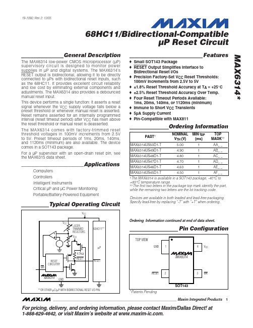
General DescriptionThe MAX6314 low-power CMOS microprocessor (µP)supervisory circuit is designed to monitor power supplies in µP and digital systems. The MAX6314’s RESET output is bidirectional, allowing it to be directly connected to µPs with bidirectional reset inputs, such as the 68HC11. It provides excellent circuit reliability and low cost by eliminating external components and adjustments. The MAX6314 also provides a debounced manual reset input.This device performs a single function: it asserts a reset signal whenever the V CC supply voltage falls below a preset threshold or whenever manual reset is asserted.Reset remains asserted for an internally programmed interval (reset timeout period) after V CC has risen above the reset threshold or manual reset is deasserted.The MAX6314 comes with factory-trimmed reset threshold voltages in 100mV increments from 2.5V to 5V. Preset timeout periods of 1ms, 20ms, 140ms,and 1120ms (minimum) are also available. The device comes in a SOT143 package.F or a µP supervisor with an open-drain reset pin, see the MAX6315 data sheet.________________________ApplicationsComputers ControllersIntelligent InstrumentsCritical µP and µC Power Monitoring Portable/Battery-Powered EquipmentFeatures♦Small SOT143 Package♦RESET Output Simplifies Interface to Bidirectional Reset I/Os♦Precision Factory-Set V CC Reset Thresholds:100mV Increments from 2.5V to 5V♦±1.8% Reset Threshold Accuracy at T A = +25°C ♦±2.5% Reset Threshold Accuracy Over Temp.♦Four Reset Timeout Periods Available: 1ms, 20ms, 140ms, or 1120ms (minimum) ♦Immune to Short V CC Transients ♦5µA Supply Current♦Pin-Compatible with MAX811MAX6314*68HC11/Bidirectional-CompatibleµP Reset Circuit________________________________________________________________Maxim Integrated Products1Pin ConfigurationTypical Operating Circuit19-1090; Rev 2; 12/05Ordering Information continued at end of data sheet.*Patents PendingFor pricing, delivery, and ordering information,please contact Maxim/Dallas Direct!at 1-888-629-4642, or visit Maxim’s website at .Ordering Information†The MAX6314 is available in a SOT143 package, -40°C to+85°C temperature range.††The first two letters in the package top mark identify the part,while the remaining two letters are the lot tracking code.Devices are available in both leaded and lead-free packaging.Specify lead-free by replacing “-T” with “+T” when ordering.M A X 631468HC11/Bidirectional-Compatible µP Reset Circuit 2_______________________________________________________________________________________ABSOLUTE MAXIMUM RATINGSELECTRICAL CHARACTERISTICS(V CC = +2.5V to +5.5V, T A = -40°C to +85°C, unless otherwise noted. Typical values are at T A = +25°C.)Stresses beyond those listed under “Absolute Maximum Ratings” may cause permanent damage to the device. These are stress ratings only, and functional operation of the device at these or any other conditions beyond those indicated in the operational sections of the specifications is not implied. Exposure to absolute maximum rating conditions for extended periods may affect device reliability.Note 1:The MAX6314 monitors V CC through an internal, factory-trimmed voltage divider that programs the nominal reset threshold.Factory-trimmed reset thresholds are available in 100mV increments from 2.5V to 5V (see Ordering and Marking Information ).Note 2:This is the minimum time RESET must be held low by an external pull-down source to set the active pull-up flip-flop.Note 3:Measured from RESET V OL to (0.8 x V CC ), R LOAD = ∞.V CC ........................................................................-0.3V to +6.0V All Other Pins..............................................-0.3V to (V CC + 0.3V)Input Current (V CC ).............................................................20mA Output Current (RESET )......................................................20mA Rate of Rise (V CC )...........................................................100V/µsContinuous Power Dissipation (T A = +70°C)SOT143 (derate 4mW/°C above +70°C).......................320mW Operating Temperature Range ...........................-40°C to +85°C Storage Temperature Range.............................-65°C to +160°C Lead Temperature (soldering, 10sec).............................+300°CMAX631468HC11/Bidirectional-CompatibleµP Reset Circuit_______________________________________________________________________________________3__________________________________________Typical Operating Characteristics(T A = +25°C, unless otherwise noted.)4.7k Ω PULL-UP 2V/divMAX6314 PULL-UP 2V/divINPUT 5V/div200ns/divPULLUP CHARACTERISTICS100pF4.7k Ω+5V74HC0574HC05V CCGNDMR 100pF+5VRESETMAX63146-50-303090SUPPLY CURRENT vs. TEMPERATURE215TEMPERATURE (°C)S U P P L Y C U R R E N T (µA )-101050347060135SUPPLY CURRENT vs. SUPPLY VOLTAGE215SUPPLY VOLTAGE (V)S U P P L Y C U R R E N T (µA )2344500-50-301090POWER-DOWN RESET DELAYvs. TEMPERATURE1040TEMPERATURE (°C)P O W E R -D O W N R E S E T D E L A Y (µs )-1020303050701.040.96-50-301090NORMALIZED RESET TIMEOUT PERIOD vs. TEMPERATURE (V CC RISING)0.970.981.021.001.03M A X 6314-05TEMPERATURE (°C)N O R M A L I Z E D R E S E T T I M E O U T P E R I O D -100.991.013050701.0060.994-50-301090NORMALIZED RESET THRESHOLD vs. TEMPERATURE (V CC FALLING)0.9960.9981.0041.000M A X 6314-06TEMPERATURE (°C)N O R M A L I Z E D R E S E T T H R E S H O L D-101.0023050701000101001000MAXIMUM TRANSIENT DURATION vs. RESET COMPARATOR OVERDRIVE20RESET COMP. OVERDRIVE, V TH - V CC (mV)M A X I M U M T R A N S I E N T D U R A T I O N (µs )4060806000-50-301090RESET PULLUP TIME vs. TEMPERATURE100200500300TEMPERATURE (°C)R E S E T P U L L -U P -T I M E (n s )-10400305070Figure 1. Functional Diagram M A X 631468HC11/Bidirectional-Compatible µP Reset Circuit 4_____________________________________________________________________________________________________________________________________________________Pin DescriptionSupply Voltage and Reset Threshold Monitor InputV CC4Manual Reset Input. A logic low on MR asserts reset. Reset remains asserted as long as MR is low, and for the reset timeout period (t RP ) after the reset conditions are terminated. Connect to V CC if not used.MR 3PIN Active-Low Complementary Output. In addition to the normal n-channel pulldown, RESET has a p-channel pullup transistor in parallel with a 4.7k Ωresistor to facilitate connection to µPs with bidirectional resets. See the Reset Output section.RESET2GroundGND 1FUNCTIONNAMEMAX631468HC11/Bidirectional-CompatibleµP Reset Circuit_______________________________________________________________________________________5Detailed DescriptionThe MAX6314 has a reset output consisting of a 4.7k Ωpull-up resistor in parallel with a P-channel transistor and an N-channel pull down (Figure 1), allowing this IC to directly interface with microprocessors (µPs) that have bidirectional reset pins (see the Reset Output section).Reset OutputA µP’s reset input starts the µP in a known state. The MAX6314 asserts reset to prevent code-execution errors during power-up, power-down, or brownout conditions. RESET is guaranteed to be a logic low for V CC > 1V (see the Electrical Characteristics table).Once V CC exceeds the reset threshold, the internal timer keeps reset asserted for the reset timeout period (t RP ); after this interval RESET goes high. If a brownout condition occurs (monitored voltage dips below its pro-grammed reset threshold), RESET goes low. Any time V CC dips below the reset threshold, the internal timer resets to zero and RESET goes low. The internal timer starts when V CC returns above the reset threshold, and RESET remains low for the reset timeout period.The MAX6314’s RESET output is designed to interface with µPs that have bidirectional reset pins, such as the Motorola 68HC11. Like an open-drain output, the MAX6314 allows the µP or other devices to pull RESET low and assert a reset condition. However, unlike a standard open-drain output, it includes the commonly specified 4.7k Ωpullup resistor with a P-channel active pullup in parallel.This configuration allows the MAX6314 to solve a prob-lem associated with µPs that have bidirectional reset pins in systems where several devices connect to RESET . These µPs can often determine if a reset was asserted by an external device (i.e., the supervisor IC)or by the µP itself (due to a watchdog fault, clock error,or other source), and then jump to a vector appropriate for the source of the reset. However, if the µP does assert reset, it does not retain the information, but must determine the cause after the reset has occurred.The following procedure describes how this is done with the Motorola 68HC11. In all cases of reset, the µP pulls RESET low for about four E-clock cycles. It then releases RESET , waits for two E-clock cycles, then checks RESET ’s state. If RESET is still low, the µP con-cludes that the source of the reset was external and,when RESET eventually reaches the high state, jumps to the normal reset vector. In this case, stored state information is erased and processing begins fromscratch. If, on the other hand, RESET is high after the two E-clock cycle delay, the processor knows that it caused the reset itself and can jump to a different vec-tor and use stored state information to determine what caused the reset.The problem occurs with faster µPs; two E-clock cycles is only 500ns at 4MHz. When there are several devices on the reset line, the input capacitance and stray capacitance can prevent RESET from reaching the logic-high state (0.8 x V CC ) in the allowed time if only a passive pullup resistor is used. In this case, all resets will be interpreted as external. The µP is guaranteed to sink only 1.6mA, so the rise time cannot be much reduced by decreasing the recommended 4.7k Ωpullup resistance.The MAX6314 solves this problem by including a pullup transistor in parallel with the recommended 4.7k Ωresis-tor (Figure 1). The pullup resistor holds the output high until RESET is forced low by the µP reset I/O, or by the MAX6314 itself. Once RESET goes below 0.5V, a com-parator sets the transition edge flip-flop, indicating that the next transition for RESET will be low to high. As soon as RESET is released, the 4.7k Ωresistor pulls RESET up toward V CC . When RESET rises above 0.5V,the active p-channel pullup turns on for the 2µs duration of the one-shot. The parallel combination of the 4.7k Ωpullup and the p-channel transistor on-resistance quickly charges stray capacitance on the reset line, allowing RESET to transition low to high with-in the required two E-clock period, even with several devices on the reset line (Figure 2). Once the one-shot times out, the p-channel transistor turns off. This process occurs regardless of whether the reset was caused by V CC dipping below the reset threshold, MR being asserted, or the µP or other device asserting RESET . Because the MAX6314 includes the standard 4.7k Ωpullup resistor, no external pullup resistor is required. To minimize current consumption, the internal pullup resistor is disconnected whenever the MAX6314asserts RESET .Manual Reset InputMany µP-based products require manual reset capabil-ity, allowing the operator, a test technician, or external logic circuitry to initiate a reset. A logic low on MR asserts reset. Reset remains asserted while MR is low,and for the reset active timeout period after MR returns high. To minimize current consumption, the internal 4.7k Ωpullup resistor on RESET is disconnected whenever RESET is asserted.M A X 631468HC11/Bidirectional-Compatible µP Reset Circuit 6_______________________________________________________________________________________MR has an internal 63k Ωpullup resistor, so it can be left open if not used. Connect a normally open momen-tary switch from MR to GND to create a manual reset function; external debounce circuitry is not required. If MR is driven from long cables or if the device is used in a noisy environment, connecting a 0.1µF capacitor from MR to ground provides additional noise immunity.__________Applications InformationNegative-Going V CC TransientsIn addition to issuing a reset to the µP during power-up,power-down, and brownout conditions, these devices are relatively immune to short-duration negative-going transients (glitches). The T ypical Operating Character-istics show the Maximum Transient Duration vs. Reset Threshold Overdrive, for which reset pulses are not generated. The graph was produced using negative-going pulses, starting at V RST max and ending below the programmed reset threshold by the magnitude indicated (reset threshold overdrive). The graph shows the maximum pulse width that a negative-going V CC transient may typically have without causing a reset pulse to be issued. As the amplitude of the transient increases (i.e., goes farther below the reset threshold),the maximum allowable pulse width decreases. A 0.1µF bypass capacitor mounted close to V CC provides addi-tional transient immunity.Ensuring a Valid RESET OutputDown to V CC = 0VWhen V CC falls below 1V, RESET no longer sinks current—it becomes an open circuit. Therefore, high-impedance CMOS-logic inputs connected to RESET can drift to undetermined voltages. This presents no problem in most applications, since most µP and other circuitry is inoperative with V CC below 1V. However, in applications where RESET must be valid down to V CC = 0V, adding a pull-down resistor to RESET will cause any stray leakage currents to flow to ground,holding RESET low (Figure 3). R1’s value is not critical;100k Ωis large enough not to load RESET and small enough to pull RESET to ground.Figure 2. MAX6314 Supports Additional Devices on the Reset BusFigure 3. RESET Valid to V CC = Ground CircuitMAX631468HC11/Bidirectional-CompatibleµP Reset Circuit_______________________________________________________________________________________7Figure 4. RESET Timing Diagram†The MAX6314 is available in a SOT143 package, -40°C to +85°C temperature range.††The first two letters in the package top mark identify the part, while the remaining two letters are the lot tracking code.†††Sample stocks generally held on the bolded products; also, the bolded products have 2,500 piece minimum-order quantities.Non-bolded products have 10,000 piece minimum-order quantities. Contact factory for details.Devices are available in both leaded and lead-free packaging. Specify lead-free by replacing “-T” with “+T” when ordering.Note:All devices available in tape-and-reel only. Contact factory for availability.___________________________________________Ordering Information (continued)M A X 631468HC11/Bidirectional-Compatible µP Reset Circuit Maxim cannot assume responsibility for use of any circuitry other than circuitry entirely embodied in a Maxim product. No circuit patent licenses are implied. Maxim reserves the right to change the circuitry and specifications without notice at any time.8_____________________Maxim Integrated Products, 120 San Gabriel Drive, Sunnyvale, CA 94086 408-737-7600©2005 Maxim Integrated ProductsPrinted USAis a registered trademark of Maxim Integrated Products, Inc._____________________________Ordering and Marking Information (continued)†The MAX6314 is available in a SOT143 package, -40°C to +85°C temperature range.††The first two letters in the package top mark identify the part, while the remaining two letters are the lot tracking code.†††Sample stocks generally held on the bolded products; also, the bolded products have 2,500 piece minimum-order quantities.Non-bolded products have 10,000 piece minimum-order quantities. Contact factory for details.Devices are available in both leaded and lead-free packaging. Specify lead-free by replacing “-T” with “+T” when ordering.Note:All devices available in tape-and-reel only. Contact factory for availability.Chip InformationTRANSISTOR COUNT: 519Package InformationFor the latest package outline information, go to /packages .。
MAX4313EUA+T中文资料
元器件交易网
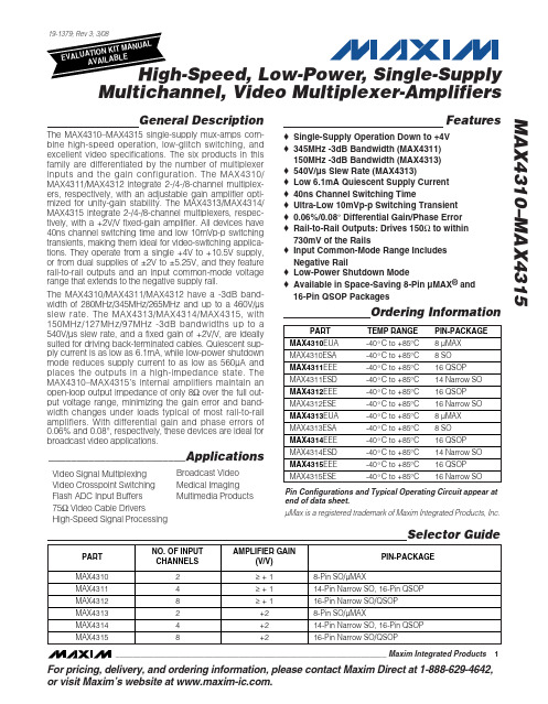
MAX4310–MAX4315
High-Speed, Low-Power, Single-Supply Multichannel, Video Multiplexer-Amplifiers
ABSOLUTE MAXIMUM RATINGS
Supply Voltage (VCC to VEE) .................................................12V Input Voltage....................................(VEE - 0.3V) to (VCC + 0.3V) All Other Pins ...................................(VEE - 0.3V) to (VCC + 0.3V) Output Current................................................................±120mA Short-Circuit Duration (VOUT to GND, VCC or VEE)....Continuous Continuous Power Dissipation (TA = +70°C)
________________________________________________________________ Maxim Integrated Products 1
For pricing, delivery, and ordering information, please contact Maxim Direct at 1-888-629-4642, or visit Maxim’s website at .
PT6314中文资料
100
90
Vin
80
9.0V
12.0V
70
15.0V
20.0V
26.0V
60
50
40
0
0.5
1
1.5
2
2.5
3
Iout-(Amps)
Efficiency - %
Efficiency vs Output Current
100
90
80
70
60
50
40
0
0.5
1
1.5
2
2.5
3
Iout-(Amps)
Vin
2
2.5
3
Iout-(Amps)
Iout-(Amps)
Thermal Derating (Ta)
3
2.5
(See Note B)
60°C 70°C
2
85°C
1.5
1
0.5
0
9
11 13 15 17 19 21 23 25 27
Vin-(Volts)
Iout-(Amps)
Thermal Derating (Ta)
元器件交易网
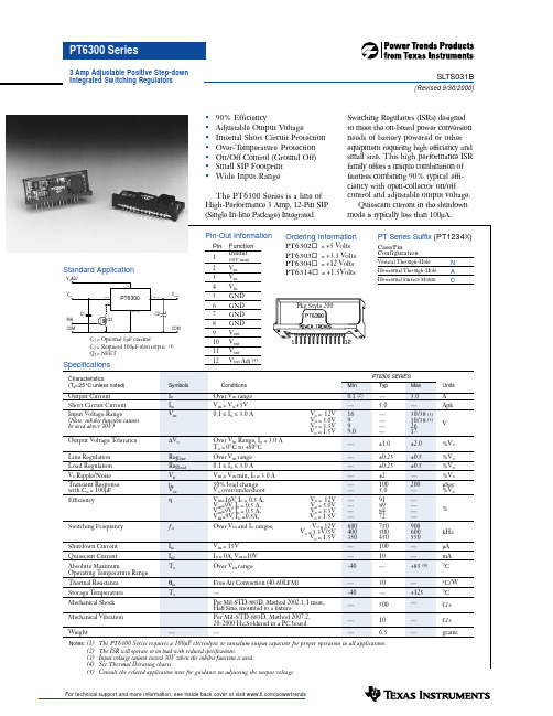
PT6300 Series
3 Amp Adjustable Positive Step-down Integrated Sw itching Regulators
SLTS031B
(Revised 9/30/2000)
• 90% Efficiency • Adjustable Output Voltage • Internal Short Circuit Protection • Over-Temperature Protection • On/Off Control (Ground Off) • Small SIP Footprint • Wide Input Range
MAX6314US29D2+T 微处理器监控电源供应电路说明书

RELIABILITY REPORTFORMAX6314US29D2+TPLASTIC ENCAPSULATED DEVICESOctober 11, 2010MAXIM INTEGRATED PRODUCTS120 SAN GABRIEL DR.SUNNYVALE, CA 94086Approved byDon LippsQuality AssuranceManager, Reliability EngineeringConclusionThe MAX6314US29D2+T successfully meets the quality and reliability standards required of all Maxim products. In addition, Maxim"s continuous reliability monitoring program ensures that all outgoing product will continue to meet Maxim"s quality and reliability standards.Table of ContentsI. ........Device Description V. ........Quality Assurance InformationII. ........Manufacturing Information VI. .......Reliability EvaluationIII. .......Packaging Information IV. .......Die Information.....AttachmentsI. Device DescriptionA. GeneralThe MAX6314 low-power CMOS microprocessor (µP) supervisory circuit is designed to monitor power supplies in µP and digital systems. TheMAX6314's active-low RESET output is bidirectional, allowing it to be directly connected to µPs with bidirectional reset inputs, such as the 68HC11. It provides excellent circuit reliability and low cost by eliminating external components and adjustments. The MAX6314 also provides a debounced manual reset input. This device performs a single function: it asserts a reset signal whenever the VCC supply voltage falls below a preset threshold or whenever manual reset is asserted. Reset remains asserted for an internally programmed interval (reset timeout period) after VCC has risen above the reset threshold or manual reset is deasserted. The MAX6314 comes with factory-trimmed reset threshold voltages in 100mV increments from2.5V to 5V. Preset timeout periods of 1ms, 20ms, 140ms, and 1120ms (minimum) are also available. The device comes in a SOT143 package. For a µP supervisor with an open-drain reset pin, see the MAX6315 data sheet.A. Description/Function: 68HC11/Bidirectional-Compatible µP Reset CircuitB. Process: B12C. Number of Device Transistors:D. Fabrication Location: Oregon or TexasE. Assembly Location: Malaysia, ThailandF. Date of Initial Production: Pre 1997III. Packaging InformationA. Package Type: 4-pin SOTB. Lead Frame: Alloy42C. Lead Finish: 100% matte TinD. Die Attach: ConductiveE. Bondwire: Au (1 mil dia.)F. Mold Material: Epoxy with silica fillerG. Assembly Diagram: #05-1601-0015H. Flammability Rating: Class UL94-V0Level 1I. Classification of Moisture Sensitivity perJEDEC standard J-STD-020-CJ. Single Layer Theta Jb: 250*°C/WK. Single Layer Theta Jc: 130°C/WL. Multi Layer Theta Ja: N/AM. Multi Layer Theta Jc: N/AIV. Die InformationA. Dimensions: 40 X 31 milsB. Passivation: Si3N4/SiO2 (Silicon nitride/ Silicon dioxide)C. Interconnect: Al/0.5%Cu with Ti/TiN BarrierD. Backside Metallization: NoneE. Minimum Metal Width: 1.2 microns (as drawn)F. Minimum Metal Spacing: 1.2 microns (as drawn)G. Bondpad Dimensions: 5 mil. Sq.H. Isolation Dielectric: SiO2I. Die Separation Method: Wafer Saw= 1= 1.83 (Chi square value for MTTF upper limit) MTTF 192 x 4340 x 443 x 2 (where 4340 = Temperature Acceleration factor assuming an activation energy of 0.8eV) A. Quality Assurance Contacts:Don Lipps (Manager, Reliability Engineering) Bryan Preeshl (Vice President of QA)B. Outgoing Inspection Level: 0.1% for all electrical parameters guaranteed by the Datasheet.0.1% For all Visual Defects.C. Observed Outgoing Defect Rate: < 50 ppmD. Sampling Plan:Mil-Std-105DVI. Reliability EvaluationA. Accelerated Life Test The results of the 135°C biased (static) life test are shown in Table 1. Using these results, the Failure Rate ( ) is calculated as follows:= 2.5 x 10-9= 2.5 F.I.T. (60% confidence level @ 25°C)The following failure rate represents data collected from Maxim"s reliability monitor program. Maxim performs quarterly life test monitors on its processes. This data is published in the Reliability Report found at /qa/reliability/monitor. ***********************************************************************@55C(0.8eV,60%UCL)B. E.S.D. and Latch-Up Testing (lot BNMAAA004GZ, D/C 9801)The MS11 die type has been found to have all pins able to withstand a HBM transient pulse of +/-2000V per Mil-Std 883 Method 3015.7. Latch-Up testing has shown that this device withstands a current of +/-250mA and overvoltage per JEDEC JESD78.Table 1Reliability Evaluation Test Results MAX6314US29D2+TTEST ITEM TEST CONDITION FAILUREIDENTIFICATION SAMPLE SIZE NUMBER OF COMMENTSFAILURESStatic Life Test (Note 1)Ta = 135°C BiasedTime = 192 hrs. DC Parameters& functionality49 0SNMBGQ001D,DC034580 0 INMBEQ001CQ, DC 991480 0NNMBDX001F,DC974177 0BNMBAB007K,DC970480 0BNMBAO001B,DC962377 0BNMAAB006L,DC9704Note 1: Life Test Data may represent plastic DIP qualification lots.。
MAX6315US27D1-T中文资料

________________General DescriptionThe MAX6315 low-power CMOS microprocessor (µP)supervisory circuit is designed to monitor power sup-plies in µP and digital systems. It provides excellent cir-cuit reliability and low cost by eliminating external components and adjustments. The MAX6315 also pro-vides a debounced manual reset input.This device performs a single function: it asserts a reset signal whenever the V CC supply voltage falls below a preset threshold or whenever manual reset is asserted.Reset remains asserted for an internally programmed interval (reset timeout period) after V CC has risen above the reset threshold or manual reset is deasserted. The MAX6315’s open-drain RESET output can be pulled up to a voltage higher than V CC .The MAX6315 comes with factory-trimmed reset thresh-old voltages in 100mV increments from 2.5V to 5V.Preset timeout periods of 1ms, 20ms, 140ms, and 1120ms (minimum) are also available. The device comes in a SOT143 package.For microcontrollers (µCs) and µPs with bidirectional reset pins, see the MAX6314 data sheet.________________________ApplicationsComputers ControllersIntelligent InstrumentsCritical µP and µC Power Monitoring Portable/Battery-Powered Equipment____________________________Featureso Small SOT143 Packageo Open-Drain RESET Output Can Exceed V CC o Precision, Factory-Set V CC Reset Thresholds:100mV Increments from 2.5V to 5V o ±1.8% Reset Threshold Accuracy at T A = +25°C o ±2.5% Reset Threshold Accuracy Over Temp.o Four Reset Timeout Periods Available: 1ms, 20ms, 140ms, or 1120ms (minimum) o Immune to Short V CC Transients o 5µA Supply Currento Pin-Compatible with MAX811MAX6315Open-Drain SOT µP Reset Circuit________________________________________________________________Maxim Integrated Products 1__________________Pin Configuration__________Typical Operating Circuit19-2000; Rev 1; 1/99Ordering and Marking Information appear at end of data sheet.For free samples & the latest literature: , or phone 1-800-998-8800.For small orders, phone 1-800-835-8769.M A X 6315Open-Drain SOT µP Reset Circuit 2_______________________________________________________________________________________ABSOLUTE MAXIMUM RATINGSELECTRICAL CHARACTERISTICS(V CC = +2.5V to +5.5V, T A = -40°C to +85°C, unless otherwise noted. Typical values are at T A = +25°C.)Stresses beyond those listed under “Absolute Maximum Ratings” may cause permanent damage to the device. These are stress ratings only, and functional operation of the device at these or any other conditions beyond those indicated in the operational sections of the specifications is not implied. Exposure to absolute maximum rating conditions for extended periods may affect device reliability.Note 1:The MAX6315 monitors V CC through an internal factory-trimmed voltage divider that programs the nominal reset threshold.Factory-trimmed reset thresholds are available in 100mV increments from 2.5V to 5V (see Ordering and Marking Information ).V CC ........................................................................-0.3V to +6.0V RESET ....................................................................-0.3V to +6.0V All Other Pins..............................................-0.3V to (V CC + 0.3V)Input Current (V CC ).............................................................20mA Output Current (RESET )......................................................20mA Rate of Rise (V CC )...........................................................100V/µsContinuous Power Dissipation (T A = +70°C)SOT143 (derate 4mW/°C above +70°C)........................320mW Operating Temperature Range ...........................-40°C to +85°C Storage Temperature Range.............................-65°C to +160°C Lead Temperature (soldering, 10sec).............................+300°CMAX6315Open-Drain SOT µP Reset Circuit_______________________________________________________________________________________360-50-303090SUPPLY CURRENT vs. TEMPERATURE215TEMPERATURE (°C)S U P P L Y C U R R E N T (µA )-101050347060135SUPPLY CURRENT vs. SUPPLY VOLTAGE215SUPPLY VOLTAGE (V)S U P P L Y C U R R E N T (µA )2344500-50-301090POWER-DOWN RESET DELAYvs. TEMPERATURE1040TEMPERATURE (°C)P O W E R -D O W N R E S E T D E L A Y (µs )-1020303050701.040.96-50-301090NORMALIZED RESET TIMEOUT PERIOD vs. TEMPERATURE (V CC RISING)0.970.981.021.001.03M A X 6315-04TEMPERATURE (°C)N O R M A L I Z E D R E S E T T I M E O U T P E R I O D-100.991.013050701.0060.994-50-301090NORMALIZED RESET THRESHOLD vs. TEMPERATURE (V CC FALLING)0.9960.9981.0041.000M A X 6315-05TEMPERATURE (°C)N O R M A L I Z E D R E S E T T H R E S H O L D-101.0023050701000101001000MAXIMUM TRANSIENT DURATION vs. RESET COMPARATOR OVERDRIVE20RESET COMP. OVERDRIVE, V TH - V CC (mV)M A X I M U M T R A N S I E N T D U R A T I O N (µs )406080__________________________________________Typical Operating Characteristics(T A= +25°C, unless otherwise noted.)______________________________________________________________Pin Description_______________Detailed DescriptionReset OutputA microprocessor’s (µP’s) reset input starts the µP in a known state. The MAX6315 asserts reset to prevent code-execution errors during power-up, power-down,or brownout conditions. RESET is guaranteed to be a logic low for V CC > 1V (see Electrical Characteristics ).Once V CC exceeds the reset threshold, the internal timer keeps reset asserted for the reset timeout period (t RP ); after this interval RESET goes high. If a brownout condition occurs (monitored voltage dips below its pro-grammed reset threshold), RESET goes low. Any time V CC dips below the reset threshold, the internal timer resets to zero and RESET goes low. The internal timer starts when V CC returns above the reset threshold, and RESET remains low for the reset timeout period.The MAX6315’s RESET output structure is a simple open-drain N-channel MOSFET switch. Connect a pull-up resistor to any supply in the 0V to +6V range. Select a resistor value large enough to register a logic low when RESET is asserted (see Electrical Characteristics ),and small enough to register a logic high while supply-ing all input current and leakage paths connected to the RESET line. A 10k Ωpull-up is sufficient in most applica-tions.Often, the pull-up connected to the MAX6315’s RESET output will connect to the supply voltage monitored at the IC’s V CC pin. However, some systems may use the open-drain output to level-shift from the monitored sup-ply to reset circuitry powered by some other supply (Figure 1). This is one useful feature of an open-drain output. Keep in mind that as the MAX6315’s V CC decreases below 1V, so does the IC’s ability to sink current at RESET . Finally, with any pull-up, RESET will be pulled high as V CC decays toward 0V. The voltage where this occurs depends on the pull-up resistor value and the voltage to which it connects (see Electrical Characteristics ).Manual-Reset InputMany µP-based products require manual-reset capabil-ity, allowing the operator, a test technician, or external logic circuitry to initiate a reset. A logic low on MR asserts reset. Reset remains asserted while MR is low,and for the reset active timeout period after MR returns high.MR has an internal 63k Ωpull-up resistor, so it can be left open if not used. Connect a normally open momen-tary switch from MR to GND to create a manual reset function; external debounce circuitry is not required.If MR is driven from long cables or if the device is used in a noisy environment, connecting a 0.1µF capacitor from MR to ground provides additional noise immunity.__________Applications InformationNegative-Going V CC TransientsIn addition to issuing a reset to the µP during power-up,power-down, and brownout conditions, these devices are relatively immune to short-duration negative-going transients (glitches). The Typical Operating Character-istics show the Maximum Transient Duration vs. Reset Threshold Overdrive, for which reset pulses are not generated. The graph was produced using negative-going pulses, starting at V RST max and ending below the programmed reset threshold by the magnitude indi-cated (reset threshold overdrive). The graph shows the maximum pulse width that a negative-going V CC tran-sient may typically have without causing a reset pulse to be issued. As the transient amplitude increases (i.e.,goes farther below the reset threshold), the maximum allowable pulse width decreases. A 0.1µF bypass capacitor mounted close to V CC provides additional transient immunity.M A X 6315Open-Drain SOT µP Reset Circuit 4_______________________________________________________________________________________Figure 1. MAX6315 Open-Drain RESET Output Allows Use with Multiple SuppliesMAX6315Open-Drain SOT µP Reset Circuit_______________________________________________________________________________________5________________________________________________________Ordering Information†The MAX6315 is available in a SOT143 package, -40°C to +85°C temperature range.††The first two letters in the package top mark identify the part, while the remaining two letters are the lot tracking code.†††Sample stocks generally held on the bolded products; also, the bolded products have 2,500 piece minimum-order quantities.Non-bolded products have 10,000 piece minimum-order quantities. Contact factory for details.Note:All devices available in tape-and-reel only. Contact factory for availability.M A X 6315Open-Drain SOT µP Reset Circuit 6__________________________________________________________________________________________________________________________________Ordering Information (continued)†The MAX6315 is available in a SOT143 package, -40°C to +85°C temperature range.††The first two letters in the package top mark identify the part, while the remaining two letters are the lot tracking code.†††Sample stocks generally held on the bolded products; also, the bolded products have 2,500 piece minimum-order quantities.Non-bolded products have 10,000 piece minimum-order quantities. Contact factory for details.Note:All devices available in tape-and-reel only. Contact factory for availability.MAX6315Open-Drain SOT µP Reset Circuit_______________________________________________________________________________________7___________________Chip InformationTRANSISTOR COUNT: 519________________________________________________________Package InformationM A X 6315Open-Drain SOT µP Reset Circuit NOTESMaxim cannot assume responsibility for use of any circuitry other than circuitry entirely embodied in a Maxim product. No circuit patent licenses are implied. Maxim reserves the right to change the circuitry and specifications without notice at any time.8_____________________Maxim Integrated Products, 120 San Gabriel Drive, Sunnyvale, CA 94086 408-737-7600©1999 Maxim Integrated ProductsPrinted USAis a registered trademark of Maxim Integrated Products.。
MAX4310中文资料

General Description
The MAX4310–MAX4315 single-supply mux-amps combine high-speed operation, low-glitch switching, and excellent video specifications. The six products in this family are differentiated by the number of multiplexer inputs and the gain configuration. The MAX4310/MAX4311/MAX4312 integrate 2-/4-/8-channel multiplexers, respectively, with an adjustable gain amplifier optimized for unity-gain stability. The MAX4313/MAX4314/MAX4315 integrate 2-/4-/8-channel multiplexers, respectively, with a +2V/V fixed-gain amplifier. All devices have 40ns channel switching time and low 10mVp-p switching transients, making them ideal for video-switching applications. They operate from a single +4V to +10.5V supply, or from dual supplies of ±2V to ±5.25V, and they feature Rail-to-Rail® outputs and an input common-mode voltage range that extends to the negative supply rail.
MAX4173

高端电流检测放大器性能分析在讨论器件功能时,检流放大器可以看作一个输入级浮空的仪表/差分放大器。
这意味着即使器件采用VCC=3.3V或5V单电源供电,在输入共模电压远高于电源电压的条件下,器件仍然能够正常放大差分输入信号。
检流放大器的共模电压可以很高,例如可以高达28V(MAX4372和MAX4173)或76V(MAX4080和MAX4081)。
检流放大器的这一特性使其非常适合高端电流检测应用,这类应用往往需要对高压侧检流电阻两端的微小电压进行放大,并馈入到低压ADC或低压模拟控制环路进行处理。
这种情况下,通常需要在信号源端(例如检流电阻两端)对电流检测信号进行滤波。
可以采用差分滤波器(图1)滤除负载电流和检流电压的“毛刺”,也可以采用共模滤波器(图2)以增强在出现共模电压尖峰或瞬时过压时的ESD保护能力。
合理选择元件构建滤波器,如果元件选择不当,则会引入一些无法预知的失调电压和增益误差,降低电路性能。
滤波器的选择MAX4173检流放大器如图3所示,该器件的检流电阻可直接连接到芯片的RS+和RS-端。
器件内部的运算放大器将检流电阻两端的差分电压恢复成RG1两端的差分电压,即ILOAD×RSENSE=VSENSE=IRG1×RG1。
然后,内部电流镜对电流IRG1进行电平转换和放大,产生输出电流IRGD。
MAX4173的内部电路中RGD=12kΩ,而RG1=6kΩ。
因此,由于RGD和RG1为片上电阻,实际阻值会因不同的半导体工艺而产生多达±30%的差异。
但是,因为最终增益精度取决于RGD和RG1的比例,所以可以很好地控制增益,并在生产过程中灵活调整。
构建差分/共模滤波器(如图1和图2所示)时,需要在检流电阻的RSENSE+和RSENSE-端与器件的RS+和RS-引脚之间接入串联电阻,此时相当于改变了芯片的RG1和RG2。
由上面的等式可知,改变后的RG1将引入增益误差。
同时,由于RG1的绝对误差最大可达±30%,因此增益误差最大将达到±30%,由于这种误差的引入是随机的,所以无法控制或估算误差。
- 1、下载文档前请自行甄别文档内容的完整性,平台不提供额外的编辑、内容补充、找答案等附加服务。
- 2、"仅部分预览"的文档,不可在线预览部分如存在完整性等问题,可反馈申请退款(可完整预览的文档不适用该条件!)。
- 3、如文档侵犯您的权益,请联系客服反馈,我们会尽快为您处理(人工客服工作时间:9:00-18:30)。
General DescriptionThe MAX6314 low-power CMOS microprocessor (µP)supervisory circuit is designed to monitor power supplies in µP and digital systems. The MAX6314’s RESET output is bidirectional, allowing it to be directly connected to µPs with bidirectional reset inputs, such as the 68HC11. It provides excellent circuit reliability and low cost by eliminating external components and adjustments. The MAX6314 also provides a debounced manual reset input.This device performs a single function: it asserts a reset signal whenever the V CC supply voltage falls below a preset threshold or whenever manual reset is asserted.Reset remains asserted for an internally programmed interval (reset timeout period) after V CC has risen above the reset threshold or manual reset is deasserted.The MAX6314 comes with factory-trimmed reset threshold voltages in 100mV increments from 2.5V to 5V. Preset timeout periods of 1ms, 20ms, 140ms,and 1120ms (minimum) are also available. The device comes in a SOT143 package.F or a µP supervisor with an open-drain reset pin, see the MAX6315 data sheet.________________________ApplicationsComputers ControllersIntelligent InstrumentsCritical µP and µC Power Monitoring Portable/Battery-Powered EquipmentFeatures♦Small SOT143 Package♦RESET Output Simplifies Interface to Bidirectional Reset I/Os♦Precision Factory-Set V CC Reset Thresholds:100mV Increments from 2.5V to 5V♦±1.8% Reset Threshold Accuracy at T A = +25°C ♦±2.5% Reset Threshold Accuracy Over Temp.♦Four Reset Timeout Periods Available: 1ms, 20ms, 140ms, or 1120ms (minimum) ♦Immune to Short V CC Transients ♦5µA Supply Current♦Pin-Compatible with MAX811MAX6314*68HC11/Bidirectional-CompatibleµP Reset Circuit________________________________________________________________Maxim Integrated Products1Pin ConfigurationTypical Operating Circuit19-1090; Rev 2; 12/05Ordering Information continued at end of data sheet.*Patents PendingFor pricing, delivery, and ordering information,please contact Maxim/Dallas Direct!at 1-888-629-4642, or visit Maxim’s website at .Ordering Information†The MAX6314 is available in a SOT143 package, -40°C to+85°C temperature range.††The first two letters in the package top mark identify the part,while the remaining two letters are the lot tracking code.Devices are available in both leaded and lead-free packaging.Specify lead-free by replacing “-T” with “+T” when ordering.M A X 631468HC11/Bidirectional-Compatible µP Reset Circuit 2_______________________________________________________________________________________ABSOLUTE MAXIMUM RATINGSELECTRICAL CHARACTERISTICS(V CC = +2.5V to +5.5V, T A = -40°C to +85°C, unless otherwise noted. Typical values are at T A = +25°C.)Stresses beyond those listed under “Absolute Maximum Ratings” may cause permanent damage to the device. These are stress ratings only, and functional operation of the device at these or any other conditions beyond those indicated in the operational sections of the specifications is not implied. Exposure to absolute maximum rating conditions for extended periods may affect device reliability.Note 1:The MAX6314 monitors V CC through an internal, factory-trimmed voltage divider that programs the nominal reset threshold.Factory-trimmed reset thresholds are available in 100mV increments from 2.5V to 5V (see Ordering and Marking Information ).Note 2:This is the minimum time RESET must be held low by an external pull-down source to set the active pull-up flip-flop.Note 3:Measured from RESET V OL to (0.8 x V CC ), R LOAD = ∞.V CC ........................................................................-0.3V to +6.0V All Other Pins..............................................-0.3V to (V CC + 0.3V)Input Current (V CC ).............................................................20mA Output Current (RESET )......................................................20mA Rate of Rise (V CC )...........................................................100V/µsContinuous Power Dissipation (T A = +70°C)SOT143 (derate 4mW/°C above +70°C).......................320mW Operating Temperature Range ...........................-40°C to +85°C Storage Temperature Range.............................-65°C to +160°C Lead Temperature (soldering, 10sec).............................+300°CMAX631468HC11/Bidirectional-CompatibleµP Reset Circuit_______________________________________________________________________________________3__________________________________________Typical Operating Characteristics(T A = +25°C, unless otherwise noted.)4.7k Ω PULL-UP 2V/divMAX6314 PULL-UP 2V/divINPUT 5V/div200ns/divPULLUP CHARACTERISTICS100pF4.7k Ω+5V74HC0574HC05V CCGNDMR 100pF+5VRESETMAX63146-50-303090SUPPLY CURRENT vs. TEMPERATURE215TEMPERATURE (°C)S U P P L Y C U R R E N T (µA )-101050347060135SUPPLY CURRENT vs. SUPPLY VOLTAGE215SUPPLY VOLTAGE (V)S U P P L Y C U R R E N T (µA )2344500-50-301090POWER-DOWN RESET DELAYvs. TEMPERATURE1040TEMPERATURE (°C)P O W E R -D O W N R E S E T D E L A Y (µs )-1020303050701.040.96-50-301090NORMALIZED RESET TIMEOUT PERIOD vs. TEMPERATURE (V CC RISING)0.970.981.021.001.03M A X 6314-05TEMPERATURE (°C)N O R M A L I Z E D R E S E T T I M E O U T P E R I O D -100.991.013050701.0060.994-50-301090NORMALIZED RESET THRESHOLD vs. TEMPERATURE (V CC FALLING)0.9960.9981.0041.000M A X 6314-06TEMPERATURE (°C)N O R M A L I Z E D R E S E T T H R E S H O L D-101.0023050701000101001000MAXIMUM TRANSIENT DURATION vs. RESET COMPARATOR OVERDRIVE20RESET COMP. OVERDRIVE, V TH - V CC (mV)M A X I M U M T R A N S I E N T D U R A T I O N (µs )4060806000-50-301090RESET PULLUP TIME vs. TEMPERATURE100200500300TEMPERATURE (°C)R E S E T P U L L -U P -T I M E (n s )-10400305070Figure 1. Functional Diagram M A X 631468HC11/Bidirectional-Compatible µP Reset Circuit 4_____________________________________________________________________________________________________________________________________________________Pin DescriptionSupply Voltage and Reset Threshold Monitor InputV CC4Manual Reset Input. A logic low on MR asserts reset. Reset remains asserted as long as MR is low, and for the reset timeout period (t RP ) after the reset conditions are terminated. Connect to V CC if not used.MR 3PIN Active-Low Complementary Output. In addition to the normal n-channel pulldown, RESET has a p-channel pullup transistor in parallel with a 4.7k Ωresistor to facilitate connection to µPs with bidirectional resets. See the Reset Output section.RESET2GroundGND 1FUNCTIONNAMEMAX631468HC11/Bidirectional-CompatibleµP Reset Circuit_______________________________________________________________________________________5Detailed DescriptionThe MAX6314 has a reset output consisting of a 4.7k Ωpull-up resistor in parallel with a P-channel transistor and an N-channel pull down (Figure 1), allowing this IC to directly interface with microprocessors (µPs) that have bidirectional reset pins (see the Reset Output section).Reset OutputA µP’s reset input starts the µP in a known state. The MAX6314 asserts reset to prevent code-execution errors during power-up, power-down, or brownout conditions. RESET is guaranteed to be a logic low for V CC > 1V (see the Electrical Characteristics table).Once V CC exceeds the reset threshold, the internal timer keeps reset asserted for the reset timeout period (t RP ); after this interval RESET goes high. If a brownout condition occurs (monitored voltage dips below its pro-grammed reset threshold), RESET goes low. Any time V CC dips below the reset threshold, the internal timer resets to zero and RESET goes low. The internal timer starts when V CC returns above the reset threshold, and RESET remains low for the reset timeout period.The MAX6314’s RESET output is designed to interface with µPs that have bidirectional reset pins, such as the Motorola 68HC11. Like an open-drain output, the MAX6314 allows the µP or other devices to pull RESET low and assert a reset condition. However, unlike a standard open-drain output, it includes the commonly specified 4.7k Ωpullup resistor with a P-channel active pullup in parallel.This configuration allows the MAX6314 to solve a prob-lem associated with µPs that have bidirectional reset pins in systems where several devices connect to RESET . These µPs can often determine if a reset was asserted by an external device (i.e., the supervisor IC)or by the µP itself (due to a watchdog fault, clock error,or other source), and then jump to a vector appropriate for the source of the reset. However, if the µP does assert reset, it does not retain the information, but must determine the cause after the reset has occurred.The following procedure describes how this is done with the Motorola 68HC11. In all cases of reset, the µP pulls RESET low for about four E-clock cycles. It then releases RESET , waits for two E-clock cycles, then checks RESET ’s state. If RESET is still low, the µP con-cludes that the source of the reset was external and,when RESET eventually reaches the high state, jumps to the normal reset vector. In this case, stored state information is erased and processing begins fromscratch. If, on the other hand, RESET is high after the two E-clock cycle delay, the processor knows that it caused the reset itself and can jump to a different vec-tor and use stored state information to determine what caused the reset.The problem occurs with faster µPs; two E-clock cycles is only 500ns at 4MHz. When there are several devices on the reset line, the input capacitance and stray capacitance can prevent RESET from reaching the logic-high state (0.8 x V CC ) in the allowed time if only a passive pullup resistor is used. In this case, all resets will be interpreted as external. The µP is guaranteed to sink only 1.6mA, so the rise time cannot be much reduced by decreasing the recommended 4.7k Ωpullup resistance.The MAX6314 solves this problem by including a pullup transistor in parallel with the recommended 4.7k Ωresis-tor (Figure 1). The pullup resistor holds the output high until RESET is forced low by the µP reset I/O, or by the MAX6314 itself. Once RESET goes below 0.5V, a com-parator sets the transition edge flip-flop, indicating that the next transition for RESET will be low to high. As soon as RESET is released, the 4.7k Ωresistor pulls RESET up toward V CC . When RESET rises above 0.5V,the active p-channel pullup turns on for the 2µs duration of the one-shot. The parallel combination of the 4.7k Ωpullup and the p-channel transistor on-resistance quickly charges stray capacitance on the reset line, allowing RESET to transition low to high with-in the required two E-clock period, even with several devices on the reset line (Figure 2). Once the one-shot times out, the p-channel transistor turns off. This process occurs regardless of whether the reset was caused by V CC dipping below the reset threshold, MR being asserted, or the µP or other device asserting RESET . Because the MAX6314 includes the standard 4.7k Ωpullup resistor, no external pullup resistor is required. To minimize current consumption, the internal pullup resistor is disconnected whenever the MAX6314asserts RESET .Manual Reset InputMany µP-based products require manual reset capabil-ity, allowing the operator, a test technician, or external logic circuitry to initiate a reset. A logic low on MR asserts reset. Reset remains asserted while MR is low,and for the reset active timeout period after MR returns high. To minimize current consumption, the internal 4.7k Ωpullup resistor on RESET is disconnected whenever RESET is asserted.M A X 631468HC11/Bidirectional-Compatible µP Reset Circuit 6_______________________________________________________________________________________MR has an internal 63k Ωpullup resistor, so it can be left open if not used. Connect a normally open momen-tary switch from MR to GND to create a manual reset function; external debounce circuitry is not required. If MR is driven from long cables or if the device is used in a noisy environment, connecting a 0.1µF capacitor from MR to ground provides additional noise immunity.__________Applications InformationNegative-Going V CC TransientsIn addition to issuing a reset to the µP during power-up,power-down, and brownout conditions, these devices are relatively immune to short-duration negative-going transients (glitches). The T ypical Operating Character-istics show the Maximum Transient Duration vs. Reset Threshold Overdrive, for which reset pulses are not generated. The graph was produced using negative-going pulses, starting at V RST max and ending below the programmed reset threshold by the magnitude indicated (reset threshold overdrive). The graph shows the maximum pulse width that a negative-going V CC transient may typically have without causing a reset pulse to be issued. As the amplitude of the transient increases (i.e., goes farther below the reset threshold),the maximum allowable pulse width decreases. A 0.1µF bypass capacitor mounted close to V CC provides addi-tional transient immunity.Ensuring a Valid RESET OutputDown to V CC = 0VWhen V CC falls below 1V, RESET no longer sinks current—it becomes an open circuit. Therefore, high-impedance CMOS-logic inputs connected to RESET can drift to undetermined voltages. This presents no problem in most applications, since most µP and other circuitry is inoperative with V CC below 1V. However, in applications where RESET must be valid down to V CC = 0V, adding a pull-down resistor to RESET will cause any stray leakage currents to flow to ground,holding RESET low (Figure 3). R1’s value is not critical;100k Ωis large enough not to load RESET and small enough to pull RESET to ground.Figure 2. MAX6314 Supports Additional Devices on the Reset BusFigure 3. RESET Valid to V CC = Ground CircuitMAX631468HC11/Bidirectional-CompatibleµP Reset Circuit_______________________________________________________________________________________7Figure 4. RESET Timing Diagram†The MAX6314 is available in a SOT143 package, -40°C to +85°C temperature range.††The first two letters in the package top mark identify the part, while the remaining two letters are the lot tracking code.†††Sample stocks generally held on the bolded products; also, the bolded products have 2,500 piece minimum-order quantities.Non-bolded products have 10,000 piece minimum-order quantities. Contact factory for details.Devices are available in both leaded and lead-free packaging. Specify lead-free by replacing “-T” with “+T” when ordering.Note:All devices available in tape-and-reel only. Contact factory for availability.___________________________________________Ordering Information (continued)M A X 631468HC11/Bidirectional-Compatible µP Reset Circuit Maxim cannot assume responsibility for use of any circuitry other than circuitry entirely embodied in a Maxim product. No circuit patent licenses are implied. Maxim reserves the right to change the circuitry and specifications without notice at any time.8_____________________Maxim Integrated Products, 120 San Gabriel Drive, Sunnyvale, CA 94086 408-737-7600©2005 Maxim Integrated ProductsPrinted USAis a registered trademark of Maxim Integrated Products, Inc._____________________________Ordering and Marking Information (continued)†The MAX6314 is available in a SOT143 package, -40°C to +85°C temperature range.††The first two letters in the package top mark identify the part, while the remaining two letters are the lot tracking code.†††Sample stocks generally held on the bolded products; also, the bolded products have 2,500 piece minimum-order quantities.Non-bolded products have 10,000 piece minimum-order quantities. Contact factory for details.Devices are available in both leaded and lead-free packaging. Specify lead-free by replacing “-T” with “+T” when ordering.Note:All devices available in tape-and-reel only. Contact factory for availability.Chip InformationTRANSISTOR COUNT: 519Package InformationFor the latest package outline information, go to /packages .。