BH1721FVC_Technicalnote_rev0.20e
17-21SURC中文资料

元器件交易网EVERLIGHT ELECTRONICS CO.,LTD.Technical Data Sheet 0805 Package Chip LED (1.0m Height)17-21SURC/S530-XX/TR8Features․Package in 8mm tape on 7〞diameter reel. ․Compatible with automatic placement equipment. ․Compatible with infrared and vapor phase reflow solder process. ․Mono-color type. ․Pb-free. ․The product itself will remain with in RoHS complaint versionDescriptions․The 17-21 SMD Taping is much smaller than lead frame type components, thus enable smaller board size, higher packing density, reduced storage space and finally smaller equipment to be obtained. ․Besides, lightweight makes them ideal for miniature applications. etc.Applications․Backlighting in dashboard and switch. ․Telecommunication: indicator and backlighting in telephone and fax. ․Flat backlight for LCD, switch and symbol. ․General use.Device Selection GuidePart No. 17-21SURC/S530-XX/TR8 Chip Material AlGaInP Emitted Color Brilliant Red Resin Color Water ClearEverlight Electronics Co., Ltd. Device No:SZDSE-171-019 Prepared date: 27-Oct-2007Rev. 2Page: 1 of 9Prepared by: Zhouhua元器件交易网EVERLIGHT ELECTRONICS CO.,LTD.17-21SURC/S530-XX/TR8Package Outline Dimensions-+1.05Note: The tolerances unless mentioned is ±0.1mm,Unit = mmEverlight Electronics Co., Ltd. Device No:SZDSE-171-019 Prepared date: 27-Oct-2007Rev. 2Page: 2 of 9Prepared by: Zhouhua元器件交易网EVERLIGHT ELECTRONICS CO.,LTD.17-21SURC/S530-XX/TR8Absolute Maximum Ratings (Ta=25℃)Parameter Reverse Voltage Forward Current Peak Forward Current (Duty 1/10 @1KHz) Power Dissipation Electrostatic Discharge(HBM) Operating Temperature Storage Temperature Soldering Temperature Symbol VR IF IFP Pd ESD Topr Tstg Tsol Rating 5 25 60 60 2000 -40 ~ +85 -40 ~ +90 Unit V mA mA mW V ℃ ℃Reflow Soldering:260 ℃ for 10 sec Hand Soldering:350℃ for 3 secElectro-Optical Characteristics (Ta=25℃)Parameter Symbol *Chip Rank Min. Typ. Max. Unit ConditionLuminous IntensityIvA2 A3 A4 A5 A6 -------------------------15 40 50 60 85 -------------------------38 60 75 90 123 140 632 624 20 2.0 -----------------------------------------2.4 10mcdViewing Angle Peak WavelengthDominant Wavelength2θ1/2 λp λd △λ VF IRdeg nm nm nm V μAIF=20 mASpectrum Radiation Bandwidth Forward VoltageReverse CurrentVR=5VEverlight Electronics Co., Ltd. Device No:SZDSE-171-019 Prepared date: 27-Oct-2007Rev. 2Page: 3 of 9Prepared by: Zhouhua元器件交易网EVERLIGHT ELECTRONICS CO.,LTD.17-21SURC/S530-XX/TR8Typical Electro-Optical Characteristics CurvesEverlight Electronics Co., Ltd. Device No:SZDSE-171-019 Prepared date: 27-Oct-2007Rev. 2Page: 4 of 9Prepared by: Zhouhua元器件交易网EVERLIGHT ELECTRONICS CO.,LTD.17-21SURC/S530-XX/TR8Label explanationCAT: Luminous Intensity Rank HUE: Dom. Wavelength Rank REF: Forward Voltage Rankxxxxxx xxxxxxRoHSxxxxxxxxxxxx xxxx xxxxxxxxReel DimensionsNote: The tolerances unless mentioned is ±0.1mm ,Unit = mmEverlight Electronics Co., Ltd. Device No:SZDSE-171-019 Prepared date: 27-Oct-2007Rev. 2Page: 5 of 9Prepared by: Zhouhua元器件交易网EVERLIGHT ELECTRONICS CO.,LTD.17-21SURC/S530-XX/TR8Carrier Tape Dimensions: Loaded quantity 3000 PCS per reelNote: The tolerances unless mentioned is ±0.1mm ,Unit = mmMoisture Resistant PackagingLabelAluminum moisture-proof bagDesiccantLabelEverlight Electronics Co., Ltd. Device No:SZDSE-171-019 Prepared date: 27-Oct-2007Rev. 2Page: 6 of 9Prepared by: Zhouhua元器件交易网EVERLIGHT ELECTRONICS CO.,LTD.17-21SURC/S530-XX/TR8Reliability Test Items And ConditionsThe reliability of products shall be satisfied with items listed below. Confidence level:90% LTPD:10%No. 1Items Reflow SolderingTest Condition Temp. : 260℃±5℃ Min. 5sec. H : +100℃ 15min ∫ 5 min L : -40℃ 15min H : +100℃ 5min ∫ 10 sec L : -10℃ 5min Temp. : 100℃ Temp. : -40℃ IF = 20 mA 85℃/ 85%RHTest Sample Hours/Cycles Size 6 Min. 300 Cycles 22 PCS.Ac/Re 0/12Temperature Cycle22 PCS.0/13Thermal Shock High Temperature Storage Low Temperature Storage DC Operating Life High Temperature / High Humidity300 Cycles 1000 Hrs. 1000 Hrs. 1000 Hrs. 1000 Hrs.22 PCS.0/14 5 6 722 PCS. 22 PCS. 22 PCS. 22 PCS.0/1 0/1 0/1 0/1Everlight Electronics Co., Ltd. Device No:SZDSE-171-019 Prepared date: 27-Oct-2007Rev. 2Page: 7 of 9Prepared by: Zhouhua元器件交易网EVERLIGHT ELECTRONICS CO.,LTD.17-21SURC/S530-XX/TR8Precautions For Use1. Over-current-proof Customer must apply resistors for protection , otherwise slight voltage shift will cause big current change ( Burn out will happen ). 2. Storage 2.1 Do not open moisture proof bag before the products are ready to use. 2.2 Before opening the package, the LEDs should be kept at 30℃ or less and 90%RH or less. 2.3 After opening the package: The LED's floor life is 1 year under 30℃or less and 60% RH orless. If unused LEDs remain, it should be stored in moisture proof packages. 2.4 If the moisture absorbent material (silica gel) has faded away or the LEDs have exceeded the storage time, baking treatment should be performed using the following conditions. Baking treatment : 60±5℃ for 24 hours. 3. Soldering Condition 3.1 Pb-free solder temperature profile3.2 Reflow soldering should not be done more than two times. 3.3 When soldering, do not put stress on the LEDs during heating. 3.4 After soldering, do not warp the circuit board.Everlight Electronics Co., Ltd. Device No:SZDSE-171-019 Prepared date: 27-Oct-2007Rev. 2Page: 8 of 9Prepared by: Zhouhua元器件交易网EVERLIGHT ELECTRONICS CO.,LTD.17-21SURC/S530-XX/TR84. Soldering Iron Each terminal is to go to the tip of soldering iron temperature less than 350℃ for 3 seconds within once in less than the soldering iron capacity 25W. Leave two seconds and more intervals, and do soldering of each terminal. Be careful because the damage of the product is often started at the time of the hand solder.5.Repairing Repair should not be done after the LEDs have been soldered. When repairing is unavoidable, a double-head soldering iron should be used (as below figure). It should be confirmed beforehand whether the characteristics of the LEDs will or will not be damaged by repairing.EVERLIGHT ELECTRONICS CO., LTD. Office: No 25, Lane 76, Sec 3, Chung Yang Rd, Tucheng, Taipei 236, Taiwan, R.O.CTel: 886-2-2267-2000, 2267-9936 Fax: 886-2267-6244, 2267-6189, 2267-6306 Everlight Electronics Co., Ltd. Device No:SZDSE-171-019 Prepared date: 27-Oct-2007Rev. 2Page: 9 of 9Prepared by: Zhouhua。
Villa Two Wire Wireless Chime Kit快速上手指南UD30792B-C说

Villa Two Wire Kit Quick Start GuideUD30792B-C©2022Hangzhou Hikvision Digital Technology Co.,Ltd.All rights reserved.About this ManualThe Manual includes instruc�ons for using and managing the Product.Pictures,charts,images and all other informa�on hereina�er are for descrip�on and explana�on only.The informa�on contained in the Manual is subject to change,without no�ce,due to firmware updates or other reasons.Please find the latest version of this Manual at the Hikvision website(h�ps:///).Please use this Manual with the guidance and assistance of professionals trained in suppor�ng the Product. Trademarksand other Hikvision’s trademarks and logos are the proper�es of Hikvision in various jurisdic�ons. Other trademarks and logos men�oned are the proper�es of their respec�ve owners.DisclaimerTO THE MAXIMUM EXTENT PERMITTED BY APPLICABLE LAW,THIS MANUAL AND THE PRODUCT DESCRIBED,WITH ITS HARDWARE,SOFTWARE AND FIRMWARE,ARE PROVIDED“AS IS”AND“WITH ALL FAULTS AND ERRORS”.HIKVISION MAKES NO WARRANTIES,EXPRESS OR IMPLIED,INCLUDING WITHOUT LIMITATION,MERCHANTABILITY,SATISFACTORY QUALITY,OR FITNESS FOR A PARTICULAR PURPOSE.THE USE OF THE PRODUCT BY YOU IS AT YOUR OWN RISK.IN NO EVENT WILL HIKVISION BE LIABLE TO YOU FOR ANY SPECIAL,CONSEQUENTIAL,INCIDENTAL,OR INDIRECT DAMAGES,INCLUDING,AMONG OTHERS, DAMAGES FOR LOSS OF BUSINESS PROFITS,BUSINESS INTERRUPTION,OR LOSS OF DATA,CORRUPTION OF SYSTEMS,OR LOSS OF DOCUMENTATION,WHETHER BASED ON BREACH OF CONTRACT,TORT(INCLUDING NEGLIGENCE),PRODUCT LIABILITY,OR OTHERWISE,IN CONNECTION WITH THE USE OF THE PRODUCT, EVEN IF HIKVISION HAS BEEN ADVISED OF THE POSSIBILITY OF SUCH DAMAGES OR LOSS.YOU ACKNOWLEDGE THAT THE NATURE OF THE INTERNET PROVIDES FOR INHERENT SECURITY RISKS,AND HIKVISION SHALL NOT TAKE ANY RESPONSIBILITIES FOR ABNORMAL OPERATION,PRIVACY LEAKAGE OR OTHER DAMAGES RESULTING FROM CYBER-ATTACK,HACKER ATTACK,VIRUS INFECTION,OR OTHER INTERNET SECURITY RISKS;HOWEVER,HIKVISION WILL PROVIDE TIMELY TECHNICAL SUPPORT IF REQUIRED.YOU AGREE TO USE THIS PRODUCT IN COMPLIANCE WITH ALL APPLICABLE LAWS,AND YOU ARE SOLELY RESPONSIBLE FOR ENSURING THAT YOUR USE CONFORMS TO THE APPLICABLE LAW.ESPECIALLY,YOU ARE RESPONSIBLE,FOR USING THIS PRODUCT IN A MANNER THAT DOES NOT INFRINGE ON THE RIGHTS OF THIRD PARTIES,INCLUDING WITHOUT LIMITATION,RIGHTS OF PUBLICITY,INTELLECTUAL PROPERTY RIGHTS,OR DATA PROTECTION AND OTHER PRIVACY RIGHTS.YOU SHALL NOT USE THIS PRODUCT FOR ANY PROHIBITED END-USES,INCLUDING THE DEVELOPMENT OR PRODUCTION OF WEAPONS OF MASS DESTRUCTION,THE DEVELOPMENT OR PRODUCTION OF CHEMICAL OR BIOLOGICAL WEAPONS,ANY ACTIVITIES IN THE CONTEXT RELATED TO ANY NUCLEAR EXPLOSIVE OR UNSAFE NUCLEAR FUEL-CYCLE,OR IN SUPPORT OF HUMAN RIGHTS ABUSES.IN THE EVENT OF ANY CONFLICTS BETWEEN THIS MANUAL AND THE APPLICABLE LAW,THE LATTER PREVAILS.Data Protec�onDuring the use of device,personal data will be collected,stored and processed.To protect data,the development of Hikvision devices incorporates privacy by design principles.For example,for device with facial recogni�on features,biometrics data is stored in your device with encryp�on method;for fingerprint device,only fingerprint template will be saved,which is impossible to reconstruct a fingerprint image.As data controller,you are advised to collect,store,process and transfer data in accordance with the applicable data protec�on laws and regula�ons,including without limita�on,conduc�ng security controls to safeguard personal data,such as,implemen�ng reasonable administra�ve and physical security controls,conduct periodic reviews and assessments of the effec�veness of your security controls.Indoor StationUser Manual of Door Station of Indoor StationOperation Guide ofIndoor StationCreate activation password for the device.8to 16characters are allowed.Enable the device Wi-Fi function,and select Wi-Fi.Enter the Wi-Fi's password.If the device has already connected to a wired network,skip the step.You can choose to reset the activation/admin password via the email or security questions if you forget your password.Choose language according to your actual needs.After language selection,you should follow the instructions to finish the wizard.Quick pairing:For normal operators who are not expert setting network parameters.indoor station and door station will be paired automatically.Set the indoor station's room No.,select door station,and indoor extension.If there are multiple door stations,tap Main to set the door station main door station.Quick pairingSet Wi-Fi4Pair Device 5Set Hik-Connect Service6PageDoor Station StatusWi-Fi Status Hik-Connect StatusAfter the devices are paired,tap Test .The video intercom will be completed done if the devices are connected properly.If exceptions occurred,the status icon will be changed at the upper right corner of the screen.Tap the icon and follow the instructions to solve.Advanced pairingabcSet Time abcdXXXX XXXX XXXXXXXXXXXXXXXX XXXX XXXX XXXX XXXX。
科迈控制器产品概述 中文

MSS不会从分支断开,当以下情况 存在时: • 并联运行激活时 • GCB打开/闭合或MCB闭合信号 激活时 • MF信号产生和GCB断开 在所的 MF解决后,GCB断开,发电机组 停止。
WebSupervisor
INTERNET
InteliCompactNT SPtM
IL-NT GPRS
出租机组
当主电源不可用或已手动切断 时,集装箱租赁发电机组和移动 发电机组为能源建设项目或土木 工程的子系统和建筑机械提临时 供必要的电源。
实际应用租赁发电机组配 备了最新的远程通信模块 InternetBridge –NT,它能控制 设备并为服务工程师提供效地监 视,控制和定位。通过使用支持 基于Web的应用软件,如
备用机组带不间断软转移功能-通过因特网远程监控
SERVICE PROVIDER INTERNET
MAINS
FIREWALL
IB-Lite
InteliCompactNT SPtM
SURGERY
GEN-SET DISTRIBUTION POINT
IGL-RA15
3台发电机组并机模式为全 部负载供电,通过IB-Lite或 IL-NT-GPRS模块,使用AirGate 技术和InteliMonitor或 WebSupervisor软件进行长时 间可靠监控。
带撤载功能备用系统 – 先进显示
ROOMS
ENGINE ROOM
InteliMIanitneslNiVT iBsiaosneB5ox +
CAN2
MAXHUB产品深度技术培训

型号
B02C SRI.SUSB.01B SRC.Camera Trans.01A SRS.HTJ41.01B
CN.SR.01A
适用机型
旗舰版 增强版/旗舰版
增强版 旗舰版 增强版/旗舰版 增强版/旗舰版 增强版/旗舰版
关键器件-MT21
关键点: 1.连接安卓转接板 2.连接PC转接板
1
2
作用: 增强PC模块到安卓模 块的信号
关键器件-VBO小板
CN.HDMI_SW.01
关键点: 1.连接TCON 2.连接HDMIOUT小板 3.连接TV主板 4.12V供电输入接口 5.PVCC 作用: 把TV板卡或者HDMI OUT 的信号传递到TCON
关键器件-MT21
关键器件-MT21
关键点: 1.无蓝牙WIFI模块 2.无天线座子 3.128G/256G SSD 4.核显 5.I5/I7 6.MD机型可选I3
PC 电源
CPU SSD
内存
关键器件-SA05
关键器件-TV板 (T.HV510.73C)
T.HV510.73
关键点: 1.连接USB HUB板 2.连接安卓转接板 3.连接VBO小板 4.连接TV电源板 5.连接USB小板,遥控头,按键板 6.连接喇叭 7.连接触摸框
问题: PC/安卓模块无信号,模块能启动
思路: ①若从开机开始就检测不到模块,有可能是安卓转接板缺陷,需要更换转接板 ②若整机静置一段时间后才检测不到模块,有可能是整机进入休眠状态。进入PC 的电源设置,把所有会导致息屏的设置都设为从不
近期案例
问题: 电磁笔书写出现跳线、无法双笔书写等与电磁笔相关的一切故障
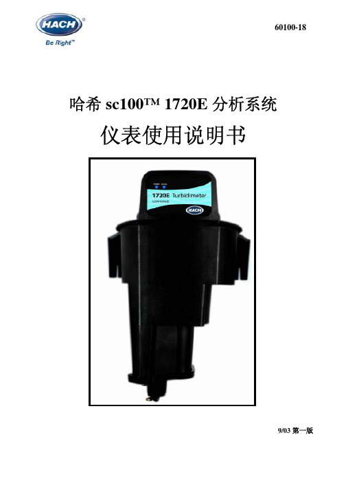
1720E浊度仪
60100-18
哈希 sc100™ 1720E 分析系统
仪表使用说明书
9/03 第一版
©哈希公司,2003 年,保留所有权利,在美国印刷
商品目录编号 60100-18
哈希 sc100™ 1720E 分析系统
仪表使用说明书
9/03 第一版
©哈希公司,2003 年,保留所有权利,在美国印刷
目录
第一节 技术规格 ....................................................................................................................................................4
LCD驱动_TM1721_datasheet

Bit1
Bit2
Bit3
Bit4
Bit5
Bit6
Bit7
位
地址
图(3)
▲注意:1、TM1721最多可以读3个字节,不允许多读。 2、读数据字节只能按顺序从BYTE1-BYTE3读取,不可跨字节读。例如:硬件上的KEY2与KS5对应按键按下
时,此时想要读到此按键数据,必须需要读到第3个字节的第6BIT位,才可读出数据; 当KEY1与KS5,KEY2与KS5,KEY3与KS5三个按键同时按下时,此时BYTE3所读数据的B5,B6,B7位均为1。
1-5 48
按键扫描信号输出
43
3V~6V
47
0V
42
内部未连线
▲ 注意:DIO口输出数据时为N管开漏输出,在读键的时候需要外接1K-10K的上拉电阻。本公司推荐10K的上拉电
阻。DIO在时钟的下降沿控制N管的动作,此时读数时不稳定,你可以参考图(6),在时钟的上升沿读数才时 稳定。
©Titan Micro Electronics V1.2
3
LCD 驱动控制专用电路
VCC
TM1721
芯片内部电路
CT
10K DIO
GND
图(1)
显示寄存器
该寄存器存储通过串行接口从外部器件传送到TM1721 的数据,地址从00H-0FH共16字节单 元,分别与芯片SGE和COM管脚所接的LCD灯对应,分配如下图: 写LCD显示数据的时候,按照从显示地址从低位到高位,从数据字节的低位到高位操作。
脚号 SSOP48
串行 数据线
2
脚号 LFQP48
说明
44
在时钟上升沿输入/输出串行数据,从低位开始。 输出为N管开漏输出,需外加上拉电阻
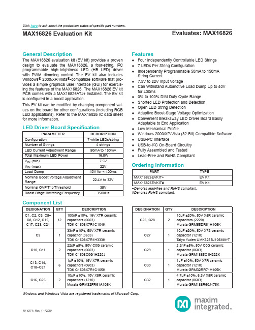
德州仪器MAX16826评估板使用手册说明书
Evaluates: MAX16826MAX16826 Evaluation KitGeneral DescriptionThe MAX16826 evaluation kit (EV kit) provides a proven design to evaluate the MAX16826, a four-string, I 2C programmable high-brightness LED (HB LED) driver with PWM dimming control. The EV kit also includes Windows ® 2000/XP/Vista ®-compatible software that pro-vides a simple graphical user interface (GUI) for exercis-ing the features of the MAX16826. The MAX16826 EV kit PCB comes with a MAX16826ATJ+ installed. The EV kit is configured in a boost application.This EV kit can be modified by changing component val -ues on the board for other configurations (including RGB LED applications). Refer to the MAX16826 IC data sheet for more information.Features●Four Independently Controllable LED Strings ●7 LEDs Per String Configuration●Independently Programmable 50mA to 150mAString Current●7.5V to 22V Input Voltage●Can Withstand Automotive Load Dump Up to 40Vfor 400ms●0% to 100% DIM Duty Cycle Range ●Shorted LED Protection and Detection ●Open LED String Detection●Adaptive Boost-Stage Voltage Optimization●Convenient Breakaway LED Driver Board EasilyAdaptable to End Application ●Low Mechanical Profile●Windows 2000/XP/Vista (32-Bit)-Compatible Software ●USB-PC Interface●USB-to-I 2C On-Board Circuitry ●Fully Assembled and Tested ●Lead-Free and RoHS Compliant19-4271; Rev 1; 12/20Windows and Windows Vista are registered trademarks of Microsoft Corp.+Denotes lead-free and RoHS compliant.#Denotes RoHS compliant.PARAMETERDESCRIPTION Configuration 7 white LEDs/stringNumber of Strings4 strings LED Current Adjustment Range 50mA to 150mATotal Maximum LED Power 16.8W V IN (min)7.5V V IN (max)22V Load Dump40V for < 400ms Nominal Boost Voltage Adjustment Range22.4V to 32VNominal OVP Trip Threshold 35V Boost Stage Switching Frequency350kHzPARTTYPE MAX16826EVKIT+EV Kit MAX16826EVKIT#EV KitDESIGNATION QTY DESCRIPTIONC1, C2, C3, C5–C8, C12, C15,C17, C23, C2412100nF ±10%, 16V X7R ceramic capacitors (0603)TDK C1608X7R1C104K C9133nF ±10%, 50V X7R ceramic capacitor (0603)TDK C1608X7R1H333K C10, C11222pF ±5%, 50V C0G ceramic capacitors (0603)TDK C1608C0G1H220J C13, C14,C18–C2161μF ±10%, 16V X7R ceramic capacitors (0603)TDK C1608X7R1C105K C16, C25210μF ±10%, 10V X5R ceramic capacitors (1210)Murata GRM32FR61A106KDESIGNATION QTY DESCRIPTIONC26, C28210μF ±20%, 50V X5R ceramic capacitors (2220)Murata GRM55DR61H106K C27110μF ±20%, 50V X7S ceramic capacitor (1210)Taiyo Yuden UMK325BJ106MM-T C2912.2nF ±5%, 50V C0G ceramic capacitor (0603)Murata GRM1885C1H222K C3011μF ±10%, 50V X7R ceramic capacitor (1210)Murata GRM32RR71H105K C3214.7μF ±10%, 6.3V X5R ceramic capacitor (0603)Murata GRM188R60J475KLED Driver Board SpecificationOrdering InformationComponent ListClick here to ask about the production status of specific part numbers.DESIGNATION QTY DESCRIPTIONC3312200pF ±10%, 50V X7R ceramic capacitor (0402)Murata GRM155R71H222KC34, C35247μF ±20%, 50V electrolytic capacitorsPanasonic EEE-FK1H470XPC36, C370Not installed, capacitors (0603)C3811000pF ±5%, 50V C0G ceramic capacitor (0402)Murata GRM1555C1H102JA01DC391220pF ±5%, 50V C0G ceramic capacitor (0402)Murata GRM1555C1H221JC401100pF ±5%, 50V C0G ceramic capacitor (0402)Murata GRM1555C1H101JC41–C4440.01μF ±10%, 50V X7R ceramic capacitors (0402)Murata GRM155R71H103KC450Not installed, capacitor (0402)D1160V, 1A Schottky diode (SMB) Diodes, Inc. B160B-13-FJ11USB series-B right-angle PC-mount receptacleJ2, J30Not installed JU2–JU873-pin headersL11Ferrite bead (0603) TDK MMZ1608R301AL2122μH ±20%, 5A, 52mΩ inductor Coilcraft MSS1260-223MlLED11Red LED (0603) Panasonic LNJ208R8ARAP1, P22Connectors, FFC/FPC 18-pos, 1mm P31Connector, FFC/FPC 6-pos, 1mmQ1140V, 9A, 2.5W n-channel MOSFET (8 SO)International Rectifier IRF7469Q2–Q5455V, 1.9A, 160mΩ n-channel MOSFET s (SOT223) International Rectifier IRFL014NPbFR11220Ω ±5% resistor (0603)R21 2.2kΩ ±5% resistor (0603)R3, R9, R103 1.5kΩ ±5% resistors (0603) R4, R5227Ω ±5% resistors (0603)R61470Ω ±5% resistor (0603)R71100kΩ ±5% resistor (0603)R817.5kΩ ±1% resistor (0603)R11168Ω ±1%, 0.25W resistor (1206)DESIGNATION QTY DESCRIPTION R1210.04Ω ±1%, 0.5W sense resistor(2010)Vishay/Dale WSL2010R0400FEA R131215kΩ ±1% resistor (0402) R14, R16210kΩ ±1% resistors (0402) R151249kΩ ±1% resistor (0402)R171 1.27kΩ ±1% resistor (0603)R181182kΩ ±1% resistor (0603)R1912kΩ ±1% resistor (0402) R20, R22,R24, R264100kΩ ±1% resistors (0402) R21, R23,R25, R27416.5kΩ ±1% resistors (0402) R28–R3142.2Ω ±1%, 100mW sense resistors(0603)Panasonic ECG ERJ-3RQF2R2V R32, R3320Ω ±5% resistors (0603)R34–R3740Ω ±5% resistors (0402)R38112.1Ω ±1% resistor (0805)R391470Ω ±5% resistor (0402)R40110kΩ ±5% resistor (0603) R41–R444237kΩ ±1% resistors (0603) U11LED driver (32 TQFN)Maxim MAX16826ATJ+ U2, U82Microcontrollers (68 QFN-EP*)Maxim MAXQ2000-RAX+ U31UART-to-USB converter (32 TQFP)FTDI FT232BLU4193C46A 3-wire EEPROM (8 SO)Atmel AT93C46A-10SU-2.7 U51p-channel MOSFET power switch(8 SO)Maxim MAX890LESA+U61LDO regulator (5 SC70)Maxim MAX8511EXK25+T U71LDO regulator (5 SC70)Maxim MAX8511EXK33+T Y1120MHz crystal oscillatorY216MHz crystalHong Kong X’talsSSL6000000E18FAF—1Cable, flat flex 18-position, 1mm, 5in—7Shunts—1USB high-speed A-to-B cable,5ft (1.5m)—1PCB: MAX16828 Evaluation Kit+Component List (continued)*Exposed pad.Quick StartRecommended EquipmentBefore beginning, the following equipment is needed: ●MAX16826 EV kit (USB cable included)● A user-supplied Windows 2000/XP/Vista PC with a spare USB port●7V to 24V, 5A DC power supply●Four strings of white LEDs (7 LEDs/string)Note: In the following sections, software-related items are identified by bolding. Text in bold refers to items directly from the EV kit software. Text in bold and underlined refers to items from the Windows operating systemProcedureThe MAX16826 EV kit is fully assembled and tested. Follow the steps below to verify board operation:1) Visit /evkitsoftware to down-load the latest version of the EV kit software,16826Rxx.ZIP (xx in the filename denotes the soft -ware version number). Save the EV kit software to a temporary folder and uncompress the ZIP file.2) Install the EV kit software on your computer by run -ning the INSTALL.EXE program inside the temporary folder. The program files are copied and icons are created in the Windows Start | Programs menu.3) Verify that all jumpers (JU2–JU8) are in their defaultpositions, as shown in Table 1.4) Connect the USB cable from the PC to the EV kitboard. A New Hardware Found window pops up when installing the USB driver for the first time. If you do not see a window that is similar to the one described above after 30 seconds, remove the USB cable from the board and reconnect it. Administra-tor privileges are required to install the USB device driver on Windows.5) Follow the directions of the Add New HardwareWizard to install the USB device driver. Choose the Search for the best driver for your device option. Specify the location of the device driver to be C:\Program Files\MAX16826 (default installation direc-tory) using the Browse button. During device driver installation, Windows may show a warning message indicating that the device driver Maxim uses does not contain a digital signature. This is not an error condi-tion and it is safe to proceed with installation. Refer to the USB_Driver_Help.PDF document included with the software for additional information.6) Set the output of the power supply to 12V. Turn offthe power supply.7) Connect the positive terminal of the power supply tothe VIN pad of the LED driver board.Note: Indicate that you are using the MAX16826 when contacting these component suppliers.SUPPLIERPHONE WEBSITECoilcraft, Diodes, Inc.Hong Kong X’tals Ltd.852-******** International RectifierMurata Electronics North America, Panasonic Taiyo Yuden TDK Vishay/Dale402-563-6866FILE DESCRIPTIONINSTALL.EXE Installs the EV kit files on your computerMAX16826.EXE Application program FTDIBUS.INF USB device driver file FTDIPORT.INF VCP device driver file UNINST.INI Uninstalls the EV kit software USB_Driver_Help.PDFUSB driver installation help fileComponent SuppliersMAX16826 EV Kit Files8) Connect the negative terminal of the power supply tothe PGND pad of the LED driver board.9) Ensure that the supplied ribbon cable is firmly con -nected to the P1 and P2 connectors.10) Connect the anode ends of the LED strings to theP3-1 pin of the P3 connector.11) Connect the cathode ends of the LED strings to theP3-2 to P3-5 pins of the P3 connector.12) Turn on the power supply13) Start the MAX16826 EV kit software by opening itsicon in the Start | Programs menu. The EV kit soft-ware main window appears, as shown in Figure 1.14) Press the Start button to start the LED driver.15) Verify that all of the LEDs are lit.Table 1. MAX16826 EV Kit Jumper Descriptions (JU2–JU8)*Default position.JUMPER SHUNT POSITIONDESCRIPTIONJU21-2*On-board PWM signal for Ch12-3Connect user-supplied PWM signal for Ch1 to the on-board DIM1 pad JU31-2*On-board PWM signal for Ch22-3Connect user-supplied PWM signal for Ch2 to the on-board DIM2 pad JU41-2*MAX16826 SDA signal connected to on-board microcontroller 2-3Connect user-supplied SDA signal to the on-board SDA pad JU51-2*MAX16826 SCL signal connected to on-board microcontroller 2-3Connect user-supplied SCL signal to the on-board SCL pad JU61-2*MAX16826 SYNC/EN signal connected to on-board microcontroller 2-3Connect user-supplied SYNC/EN signal to the on-board SYNC/EN pad JU71-2*On-board PWM signal for Ch32-3Connect user-supplied PWM signal for Ch3 to the on-board DIM3 pad JU81-2*On-board PWM signal for Ch42-3Connect user-supplied PWM signal for Ch4 to the on-board DIM4 padDetailed Description of SoftwareThe MAX16826 evaluation kit software has all the functions to evaluate the MAX16826 IC. To start the MAX16826 EV kit software, click Start | Programs | Maxim MAX16826 Evaluation Kit | Maxim MAX16826 Evaluation Kit that is created during installation. The GUI main window appears as shown in Figure 1.Figure 1. MAX16826 EV Kit Software Main WindowString Current SetThe String Current Set group box is located at the upperleft corner of the main window. Use the scrollbars toadjust the current of the LED strings. The correspondingvalues of the current will be shown in the adjacent editboxes. Press the Read button to read the values from thelinear regulator output registers of the MAX16826. Theequivalent values of the output current will be shown inthe edit boxes.Boost Output ControlThe Boost Output Control Mode group box has thefunctions to control the boost output voltage.To control the boost output voltage manually, click on theradio button next to the Manual Control group box. Usethe scrollbar to adjust the output voltage, and the volt-age value will be displayed in the adjacent edit box. Theactual boost output voltage can be seen in the Read BackValues group box.To use the software automatic control, click on the radiobutton next to the Software Control group box. The editbox next to the Set button is used to change the Drain toGND regulated voltage of the current sink FETs on the LEDstring with the highest voltage drop. This voltage setting willdepend on how much overhead the user is willing to have.If the set value is too low, the LED currents will no longerbe well regulated and may indeed drop because the boostvoltage might fall too low. The scrollbar in this mode willmove automatically to compensate and regulate the outputvoltage. The update rate is approximately once per second.In any case, the channel with the lowest voltage across thesink FET will be regulated to the value in the edit box. DIM Pulse Width Modulation (DPWM)The DPWM group box is located at the center of the mainwindow. The four DIM PWM signals generated by theon-board MAXQ2000 microcontrollers are used to controlthe brightness of the LEDs. Adjust the scrollbars in theDPWM Duty Cycle group box to change the duty cycles of the PWM signals and the values of the duty cycle (%)are shown in the adjacent edit boxes. Check the Set AllChannels to 100% Duty Cycle checkbox to force all channel duty cycles to 100%.In the DPWM Frequency group box, change the DPWMfrequency by adjusting the scrollbar position and pressthe Set button. The frequency value will be shown in theedit box.To guarantee that the leading edge of all the DIM signalsare synchronized, press the Set button in the DPWMFrequency group box.Press the Start button to start to generate the PWM signals.Press the Stop button to stop all PWM signals.StatusThe Status group box is located at the right of the main window. The software reads the external FET drain voltage measurements, and the boost output voltage measurement from the ADC output registers of the MAX16826. The software multiplies the measured values by the appropriate scaling factor and then displays them in the Read Back Values group box.Enter the values into the edit boxes in the Fault Level Set group box to set the fault-detection values. When the value in the Read Back Values group box is less than the fault-detection value, then the color of the read-back value changes to dark green. When the read-back value is 0 to 10% higher than the fault-detection value, the read-back value turns a lime color. If the read-back value is more than 10% higher than the fault-detection value, then the read-back value turns purple. The read-back value turns red when it is more than 20% higher than the fault-detection value.The software also reads the fault register to detect the fault conditions. If a fault condition exists, it will be shown in the String Fault Status group box. See Table 2 for the fault-condition explanations.Press the Read button to update the Status group box. By checking the Automatic Read checkbox, the Status group box will be automatically updated every second. Enable/DisableThe Enable/Disable group box controls the signal on the SYNC/EN pin. Click on the Enable radio button to set the signal high and enable the MAX16826. Click on the Disable radio button to set the signal low and disable the MAX16826.StandbyCheck the Standby checkbox to set the MAX16826 to standby mode. Refer to the MAX16826 IC data sheet for more information regarding standby mode.Table 2. Fault Conditions*Open LED string detection may require multiple flag examination. FAULT NAME CONDITIONTOADC conversion timeout; alsocorresponds to open string condition* Open LED string openShort LED string shortedOVP OvervoltageScaling FactorsThe calculations for the LED string current, boost output voltage, and the read-back values are based on the scal-ing factors. You can change the scaling factor by select-ing the Scaling Factor menu item under the Scaling Factors menu bar. In the pop-up window shown in Figure 2, enter the appropriate scaling factor.See Table 3 for the formulas for the scaling factors. These values can be used for calibration against actual read values with external instruments.When the default values are changed, they are stored in the software. Re-enter the default values to bring the software back to the default setting.Table 3. Scaling FactorFigure 2. Scaling Factor WindowSCALING FACTOR FORMULADEFAULTVALUE DR1 (ADC read-back voltageacross Drain and GND for thesink FET on Ch1)1 + (R20/R21)7.046DR2 (ADC read-back voltageacross Drain and GND for thesink FET on Ch2)1 + (R22/R23)7.046DR3 (ADC read-back voltageacross Drain and GND for thesink FET on Ch3)1 + (R24/R25)7.046DR4 (ADC read-back voltageacross Drain and GND for thesink FET on Ch4)1 + (R26/R27)7.046Read Back VBoost (ADC read-back boost output voltage)1 + (R15/R16)25.900 String Current Set Ch1 (LEDstring current for Ch1)R31 2.200 String Current Set Ch2 (LEDstring current for Ch2)R30 2.200 String Current Set Ch3 (LEDstring current for Ch3)R29 2.200 String Current Set Ch4 (LEDstring current for Ch4)R28 2.200 VBoost (Boost output voltage) 1 + (R13/R14)22.500Detailed Description of HardwareThe MAX16826 EV kit board provides a proven layout for evaluating the MAX16826 IC. This EV kit consists of a controller board and an LED driver board. The break-away slots at the center of the EV kit make it easier for the user to break and separate the controller board from the LED driver board. This is done so that once the evaluation is complete with the included software, the driver board can easily be used in the target application environment with the target system microcontroller.To connect the power, ground, PWM, and the I2C inter-face signals of the boards, attach the ribbon cable to the P1 connector of the controller board and attach the other end of the ribbon cable to the P2 connector of the LED driver board.Controller BoardThe controller board acts as the bridge between the soft-ware in the PC and the actual LED driver board containing the MAX16826. In addition to the USB connectivity, it gen-erates the four adjustable PWM DIM signals that control the brightness of the LEDs. The controller board com-municates with the driver board through the I2C interface, and is able to read or change the values of the registers in the MAX16826.The user can use the MAX16826 evaluation kit software to control the controller board.See Table 1 to control the MAX16826 with a user-supplied PWM signal.LED Driver BoardThe LED driver board is able to drive up to four LED strings (7 LEDs/string). LED strings can be connected to the LED driver board through the P3 connector by using a ribbon cable. Connect all of the anode ends of the LED strings to the P3-1 pin (which connects to the boost out-put) of the P3 connector. Then connect the cathode ends of the LED strings to the P3-2 to P3-5 pins (that connects to the drains of the sink FETs) of the P3 connector. User-Supplied I2C InterfaceTo use the MAX16826 EV kit with a user-supplied I2C interface, install the shunts on pins 2-3 of JU4 and JU5. Connect SDA, SCL, and GND lines from the usersupplied I2C interface to the SDA, SCL, and PGND pads on the MAX16826 controller board.After the LED driver board has broken away from the controller board, the user may connect their supplied I2C, DIM, and power signals to the LED driver board through the P2 connector using a ribbon cable. See Table 4 for the pin description of the P2 connector.Table 4. Pin Description for P2 Connector PIN NUMBER DESCRIPTIONP2-1 to P2-5Connect to the VIN pin of the MAX16826 P2-6Not connectedP2-7 to P2-11Connect to the groundP2-12Connects to the SYNC/EN pin of theMAX16826P2-13Connects to the SDA pin of the MAX16826P2-14Connects to the SCL pin of the MAX16826P2-15Connects to the DIM4 pin of the MAX16826P2-16Connects to the DIM3 pin of the MAX16826P2-17Connects to the DIM2 pin of the MAX16826P2-18Connects to the DIM1 pin of the MAX16826Figure 3. MAX16826 EV Kit LED Driver Board SchematicFigure 4a. MAX16826 EV Kit Controller Board Schematic (Sheet 1 of 2)Figure 4b. MAX16826 EV Kit Controller Board Schematic (Sheet 2 of 2)Maxim Integrated cannot assume responsibility for use of any circuitry other than circuitry entirely embodied in a Maxim Integrated product. No circuit patent licenses are implied. Maxim Integrated reserves the right to change the circuitry and specifications without notice at any time.REVISIONNUMBERREVISION DATE DESCRIPTION PAGES CHANGED 009/08Initial release —112/20Updated Ordering Information 1Revision HistoryFor pricing, delivery, and ordering information, please visit Maxim Integrated’s online storefront at https:///en/storefront/storefront.html.。
BH1710_BH1750应用手册V1.0

150%
200%
BH1710FVC
最小值
最大值
153.00% 00110_00100b
29% 11111_11110b
10 进 制值
2 进制值
寄存器 高8位
值
寄存器 低8位
值
300 01001_01100 600 10010_11000
0x49 0x52
0x6c 0x78
375 01011_10111 0x4b 250 00111_11010 0x47 200 00110_01000 0x46
ROHM CO., LTD
4
Ver 1.0 - (Jan-2009)
Generated by Foxit PDF Creator © Foxit Software For evaluation only.
BH1710/BH1750 应用手册
BH1710FVC/BH1750FVI
应用手册
ROHM CO., LTD
1
Ver 1.0 - (Jan-2009)
Generated by Foxit PDF Creator © Foxit Software For evaluation only.
BH1710/BH1750 应用手册
目录
1 参考设计图....................................................................................................................................................1 2 解析度(Resolution)设置...........................................................................................................................3 3 透光率设置....................................................................................................................................................4 4 光亮度值计算方法........................................................................................................................................5 5 参考软件代码................................................................................................................................................6
- 1、下载文档前请自行甄别文档内容的完整性,平台不提供额外的编辑、内容补充、找答案等附加服务。
- 2、"仅部分预览"的文档,不可在线预览部分如存在完整性等问题,可反馈申请退款(可完整预览的文档不适用该条件!)。
- 3、如文档侵犯您的权益,请联系客服反馈,我们会尽快为您处理(人工客服工作时间:9:00-18:30)。
Digital
Serial Output Type
BH1721FVC
All data on this sheet are specified as Target. This subject to change without notice. In your actual designing, please refer to latest version.
AMP Integration-OPAMP for converting from PD current to Voltage.
ADC AD converter for obtainment Digital 16bit data.
Logic + I2C Interface Ambient Light Calculation and I2C BUS Interface. It is including below register. Data Register ˠ This is for registration of Ambient Light Data. Initial Value is "0000_0000_0000_0000".
0 0 8 16 24 32 40 48 56 64 Illuminance [ lx ]
Fig.2 Illuminance – Measurement Result 1
1.2
1
Ratio
0.8 ҉ిྲྀԹಛ
0.6 -
0.4
-
1pin
0.2
+
+
0
-90 -60 -30
0
30 60 90
Angle [ deg ]
rIF
ʵ
Typ. 140 0.01 560 1.2
0 1 8 120 16
1
Max. 199 1.0 ʵ 1.38
2 ʵ ʵ 180 24
ʵ
Units Conditions
uA
Ev = 100 lx ˞1
uA No input Light
nm times count
Sensor out / Actual lx EV = 1000 lx ˞1, ˞2
tSUDAT
100
ʵ
ʵ
ns
I2C ‘L’ Period of the SCL Clock
tLOW
1.3
ʵ
ʵ
us
I2C ‘H’ Period of the SCL Clock
tHIGH
0.6
ʵ
ʵ
us
I2C SDA Output ‘L’ Voltage
VOL
0
ʵ
0.4
V
IOL = 3 mA
˞1 White LED is used as optical source. ˞2 Measurement Accuracy typical value is possible to change '1' by "Measurement result adjustment function". ˞3 Use H-Resolution Mode if dark data ( less than 10 lx ) is need.
Fig.5 Directional Characteristics 2
Ratio
1.4
1.2
1
0.8
0.6
0.4
0.2
0 -40 -20 0 20 40 60 80 100 Ta [ ˆ ]
Fig.8 Light Source Dependency ( Fluorescent Light is set to '1' )
Parameter
Symbol Min.
Typ.
Max. Units
VCC Voltage
Vcc
2.4
3.0
3.6
V
I2C Reference Voltage
VDVI
1.65
ʵ
VCC
V
1 / 15
Feb. 26. 2009 0.20e
˔ Electrical Characteristics ( VCC = 3.0V, DVI = 3.0V, Ta = 25ˆ, unless otherwise noted )
10
ICC @ POWER DOWN [ uA ]
1
0.1
0.01
-40
-20
0
20
40
60
80
Ta [ ˆ ]
Fig.10 VCC – ICC@0 Lx ( POWER DOWN )
Measurement Result
64
56
48
40
32
24 HH-R-Reess..
L-Res.
16
8 L-Res.
VIL1
SCL, SDA Input ‘L’ Voltage 2
VIL2
SCL, SDA, Input ‘H’ Current
IIH
SCL, SDA, Input ‘L’ Current
I2C SCL Clock Frequency
I2C Bus Free Time
I2C Hold Time ( repeated ) START Condition I2C Set up time for a Repeated START Condition I2C Set up time for a Repeated STOP Condition
˔ Absolute Maximum Ratings
Parameter
Symbol
Limits
Units
Supply Voltage
Vmax
4.5
V
Operating Temperature
Topr
-40ʙ85
ˆ
Storage Temperature
Tstg
-40ʙ100
ˆ
SDA Sink Current
+ 0.6
0.4
-
+
0.2
0
-90 -60 -30
0
30 60 90
Angle [ deg ]
Fig.4 Directional Characteristics 1
Ratio
1.2
1
0.8
0.6
0.4
0.2
0
-40
-10
20
50
Ta [ ˆ ]
80
110
Fig.7 Measurement Result Temperature Dependency
10) Small measurement variation (+/- 15%) 11) Compact surface mount package 1.6 x 1.6 x 0.55 mm
˔ Applications Mobile phone, LCD TV, NOTE PC, Portable game machine, Digital camera, Digital video camera, Car navigation, PDA, LCD display
200
150 VCC vs ICC@ ଌ ఆ த
100
50
0
2
2.5
3
3.5
4
VCC [ V ]
Fig.9 VCC – ICC ( During measurement )
1.2
1
VCC=3V
0.8
0.6
0.4
0.2
0
1.5
2
2.5
3
3.5
DVI [ V ]
Fig.12 Measurement Result
DVI Dependency
3 / 15
˔ Block Diagram
VCC
DVI
AMP PD
ç ADC
Logic +
I2C Interface
OSC GND
SCL SDA
˔ Block Diagram Descriptions
PD Photo diode with approximately human eye response.
Parameter Supply Current Powerdown Current Peak Wave Length
Measurement Accuracy
Symbol
Min.
Icc1
ʵ
Icc2
ʵ
Еp
ʵ
S/A
1.02
Dark ( 0 lx ) Sensor out
S0
0
H-Resolution Mode Resolution
Imax
7
mA
Power Dissipation
Pd
165˞
mW
˞ 70mm ʷ 70mm ʷ 1.6mm glass epoxy board. Derating in done at 2.2mW/ˆ for operating above Ta=25ˆ.
˔ Operating Conditions
I2C Data Hold Time
IIL fSCL tBUF tHDSTA tSUSTA tSUSTO tHDDAT
0.7 * DVI 1.26 ʵ ʵ ʵ ʵ ʵ 1.3 0.6
0.6
0.6
0
ʵ
ʵ
V
DVI ʾ 1.8V
ʵ