1N3344B中文资料
TN-124中文资料

DESCRIPTIONSPECIFICATION RANGESAPPLICATIONSFEATURESCP Clare’s TD Series of gas discharge microwave noise tubes and TN Series of gas discharge microwave noise sources are the element in a microwave RF system that allows accurate measurements of the noise figure of the receiver or its components. The requirements of a device used for making such noise figure measurements include broad bandwidth inherent in the active element, stability, ease of operation, and long life. In general, the range of usefulness of these noise sources permits measurements of noise figures from about 2 to 30dB. The PS-237 through PS-240 current-regulated power supplies can be used to operate many of the noise sourcesdescribed herein.s Excess noise ratios (ENR): up to 20dB s Broad bandwidths Excellent long term stability s Life up to 20,000 hourssAC, DC, or pulsed operationsNoise figure measurementrequirements not listed.)TD SERIES GAS DISCHARGE NOISE SOURCE TUBESwith Filamentary or Hollow CathodesAC,DC operation — cathodes at both ends.Pulse operation — cathode at one end specially designed for pulse operation. If the anode current during the “on” time of a square wavepulse (>100µs duration) is nominally the same as the rated DC anode current, the tube drop during this period will be approximately the same as the rated DC tube drop.(2)Excess noise ratio of tube only.TD SERIES GAS DISCHARGE NOISE SOURCE TUBESwith Indirectly-Heated CathodesAll characteristics at 25˚C.OUTLINE DRAWINGS (Noise Source Tubes with Filamentary or Hollow Cathodes)(3)The “a” suffix indicates using the bi-pin termination depicted in the inset labelled “AL T.-A”.(4)The diameter of the tube shall not exceed this value over the length of the tube denoted in the figure by “B”.TD SERIES GAS DISCHARGE NOISE SOURCE TUBESwith Indirectly-Heated Cathodes(5)All characteristics at 25˚C.(5) CP Clare can usually refurbish noise sources (depending on condition of waveguide) and install replacement tubes.TD SERIES GAS DISCHARGE NOISE SOURCE TUBESwith Filamentary Cathode Noise Tubes(5)All characteristics at 25˚CNOISE SOURCE POWER SUPPLIESwith Current Regulation(6) These power supplies, though designed for the TN-162 through TN-173, are capable of operating many other noise sources made by CP Clare.ORDERING INFORMATIONA complete part number is represented bythe information in the Part Number columnof the specification table.。
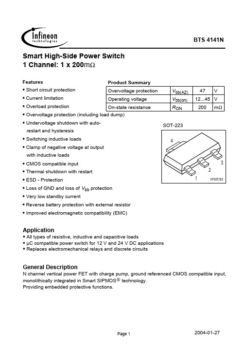
BTS4141N中文资料
Value
Unit
-0,31)...48
V
-10...Vbb
self limited
A
±5
mA
-0.5
A
internal limited °C
-55 ... +150
1.4
W
0.7
J
V
83 kV
±1 ±5
1defined by Ptot 2At VIN > Vbb, the input current is not allowed to exceed ±5 mA. 3defined by Ptot 4Device on 50mm*50mm*1.5mm epoxy PCB FR4 with 6 cm2 (one layer, 70µm thick) copper area for Vbb connection. PCB is vertical without blown air. 5not subject to production test, specified by design 6VLoaddump is setup without the DUT connected to the generator per ISO 7637-1 and DIN 40839 . Supply voltages higher than Vbb(AZ) require an external current limit for the GND pin, e.g. with a 150Ω resistor in GND connection. A resistor for the protection of the input is integrated.
General Description
1N4148,1N4448中文资料

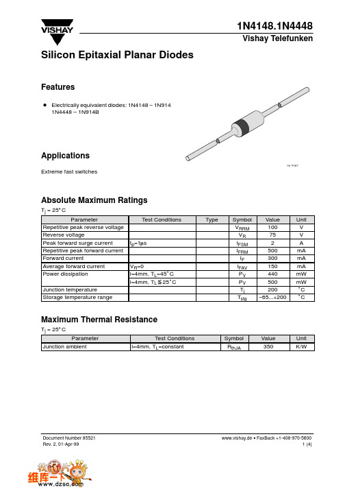
封装: DO-35 玻璃封装 Case: DO-35 Glass Case
Unit:mm
极性: 色环端为负极 Polarity: Color band denotes cathode end 安装位置: 任意 Mounting Position: Any
极限值和温度特性 TA = 25℃ 除非另有规定。 Maximum Ratings & Thermal Characteristics Ratings at 25℃ ambient temperature unless otherwise specified.
不重复峰值反向电压 Non-repetitive Peak Reverse Voltage
反向峰值电压 peak repetitive Reverse Voltage 最大正向平均电流 Forward Continuous Current 平均整流输出电流 Average Rectified Output Current
1N4148 / 1N4448
DO-35 Glass
max. 0.52
小信号肖特基二极管 Small Signal Schottky Diodes
特征 Features
1.8 0.2
CATHODE MARK
min. 27.5 3.8 0.2 min. 27.5
·反向漏电流小。Low reverse leakage ·开关速度快。Fast switching speed ·最大功率耗散500mW。Maximum power dissipation 500mW ·高稳定性和可靠性。High stability and high reliability
符号
NB4N11M资料

NB4N11M3.3 V 2.5 Gb/s Multi Level Clock/Data Input to CML Receiver/ Buffer/ TranslatorDescriptionT h e NB4N11M i s a d iff e r e n tia l 1−to−2 c lo c k/d a ta distribution/translation chip with CML output structure, targeted for high−speed clock/data applications. The device is functionally equivalent to the EP11, LVEP11, SG11 or 7L11M devices. Device produces two identical differential output copies of clock or data signal operating up to 2.5 GHz or 2.5 Gb/s, respectively. As such, NB4N11M is ideal for SONET, GigE, Fiber Channel, Backplane and other clock/data distribution applications.Inputs accept LVPECL, CML, LVCMOS, LVTTL, or LVDS (See Table 5). The CML outputs are 16 mA open collector (See Figure 18) which requires resistor (R L) load path to V TT termination voltage. The open collector CML outputs must be terminated to V TT at power up. Differential outputs produces current–mode logic (CML) compatible levels when receiver loaded with 50 W or 25 W loads connected to 1.8 V, 2.5 V or 3.3 V supplies (see Figure 19). This simplifies device interface by eliminating a need for coupling capacitors.The device is offered in a small 8−pin TSSOP package. Application notes, models, and support documentation are available at .Features•Maximum Input Clock Frequency > 2.5 GHz •Maximum Input Data Rate > 2.5 Gb/s•Typically 1 ps of RMS Clock Jitter•Typically 10 ps of Data Dependent Jitter @ 2.5 Gb/s, R L = 25 W •420 ps Typical Propagation Delay•150 ps Typical Rise and Fall Times•Operating Range: V CC = 3.0 V to 3.6 V with V EE = 0 V andV TT = 1.8 V to 3.6 V•Functionally Compatible with Existing 2.5 V / 3.3 V LVEL, LVEP, EP, and SG Devices•These are Pb−Free Devices**For additional information on our Pb−Free strategy and soldering details, please download the ON Semiconductor Soldering and Mounting Techniques Reference Manual, SOLDERRM/D.See detailed ordering and shipping information in the package dimensions section on page 10 of this data sheet.ORDERING INFORMATIONFigure 2. Pinout (Top View) and Logic DiagramDV EEV CCQ0DQ1Q1Q0Table 1. Pin DescriptionPin Name I/O Description1Q0CML OutputNoninverted differential output. Typically receiver terminated with 50 W resistor to V TT . Open collector CML outputs must be terminated to V TT at powerup.2Q0CML Output Inverted differential output. Typically receiver terminated with 50 W resistor to V TT . Open collector CML outputs must be terminated to V TT at powerup.3Q1CML OutputNoninverted differential output. Typically receiver terminated with 50 W resistor to V TT . Open collector CML outputs must be terminated to V TT at powerup.4Q1CML OutputInverted differential output. Typically receiver terminated with 50 W resistor to V TT . Open collector CML outputs must be terminated to V TT at powerup.5V EE −Negative supply voltage.6D LVPECL, CML, HSTL,LVCMOS, LVDS, LVTTL Input Inverted differential input.7D LVPECL, CML, HSTL,LVCMOS, LVDS, LVTTL InputNoninverted differential input.8V CC−Positive supply voltage.Table 2. ATTRIBUTESCharacteristics ValueESD Protection Human Body ModelMachine Model > 1000 V > 70 VMoisture Sensitivity (Note 1)8−TSSOP Level 1Flammability Rating Oxygen Index: 28 to 34UL 94 V−0 @ 0.125 inTransistor Count197Meets or exceeds JEDEC Spec EIA/JESD78 IC Latchup Test1.For additional information, see Application Note AND8003/D.Table 3. MAXIMUM RATINGSSymbol Parameter Condition 1Condition 2Rating Unit V CC Positive Power Supply V EE = −0.5 V4V V EE Negative Power Supply V CC = +0.5 V−4VV I Positive InputNegative Input V EE = 0 VV CC = 0 VV I = V CC+0.4 VV I = V EE –0.4 V4−4VVV O Output Voltage MinimumMaximum V EE + 600V CC + 400mVmVT A Operating Temperature Range−40 to +85°C T stg Storage Temperature Range−65 to +150°Cq JA Thermal Resistance (Junction−to−Ambient) (Note 2)0 lfpm500 lfpmTSSOP−8TSSOP−8190130°C/W°C/Wq JC Thermal Resistance (Junction−to−Case)1S2P (Note 2)TSSOP−841 to 44°C/W T sol Wave Solder< 3 Sec @ 260°C265°C Maximum ratings are those values beyond which device damage can occur. Maximum ratings applied to the device are individual stress limit values (not normal operating conditions) and are not valid simultaneously. If these limits are exceeded, device functional operation is not implied, damage may occur and reliability may be affected.2.JEDEC standard multilayer board − 1S2P (1 signal, 2 power) with 8 filled thermal vias under exposed pad.Table 4. DC CHARACTERISTICS, CLOCK Inputs, CML Outputs V CC = 3.0 V to 3.6 V, V EE = 0 V, T A = −40°C to +85°C Symbol Characteristic Min Typ Max Unit I CC Power Supply Current (Inputs and Outputs Open)2535mA R L = 50 W, V TT = 3.6 V to 2.5 VV OH Output HIGH Voltage (Note 3)V TT− 60V TT− 10V TT mV V OL Output LOW Voltage (Note 3)V TT− 1100V TT− 800V TT− 640mV |V OD|Differential Output Voltage Magnitude6407801000mV R L = 25 W, V TT = 3.6 V to 2.5 V $5%V OH Output HIGH Voltage (Note 3)V TT− 60V TT− 10V TT mV V OL Output LOW Voltage (Note 3)V TT− 550V TT− 400V TT− 320mV |V OD|Differential Output Voltage Magnitude320390500mV R L = 50 W, V TT = 1.8 V $5%V OH Output HIGH Voltage (Note 3)V TT− 170V TT− 10V TT mV V OL Output LOW Voltage (Note 3)V TT− 1100V TT− 800V TT− 640mV |V OD|Differential Output Voltage Magnitude5707801000mV R L = 25 W, V TT = 1.8 V $5%V OH Output HIGH Voltage (Note 3)V TT− 85V TT− 10V TT mV V OL Output LOW Voltage (Note 3)V TT− 500V TT− 400V TT− 320mV |V OD|Differential Output Voltage Magnitude285390500mV DIFFERENTIAL INPUT DRIVEN SINGLE−ENDED (Figures 14 and 16)V th Input Threshold Reference Voltage Range (Note 5)V EE V CC mV V IH Single−ended Input HIGH Voltage V th + 100V CC + 400mV V IL Single−ended Input LOW Voltage V EE− 400V th− 100mV DIFFERENTIAL INPUTS DRIVEN DIFFERENTIALLY (Figures 15 and 17)V IHD Differential Input HIGH Voltage V EE V CC + 400mV V ILD Differential Input LOW Voltage V EE− 400V CC− 100mV V CMR Input Common Mode Range (Differential Configuration)V EE V CC mV |V ID|Differential Input Voltage Magnitude (|V IHD− V ILD|) (Note 7)100V CC− V EE mV C IN Input Capacitance (Note 7) 1.5pF NOTE:Device will meet the specifications after thermal equilibrium has been established when mounted in a test socket or printed circuit board with maintained transverse airflow greater than 500 lfpm. Electrical parameters are guaranteed only over the declaredoperating temperature range. Functional operation of the device exceeding these conditions is not implied. Device specification limit values are applied individually under normal operating conditions and not valid simultaneously.3.CML outputs require R L receiver termination resistors to V TT for proper operation. Outputs must be connected through R L to V TT at powerup. The output parameters vary 1:1 with V TT.4.Input parameters vary 1:1 with V CC.5.V th is applied to the complementary input when operating in single−ended mode.6.V CMR (MIN) varies 1:1 with V EE, V CMR max varies 1:1 with V CC.7.Parameter guaranteed by design and evaluation but not tested in production.Table 5. AC CHARACTERISTICS V CC = 3.0 V to 3.6 V, V EE = 0 V; (Note 8)Symbol Characteristic−40°C25°C 85°C Unit Min Typ MaxMin Typ MaxMin Typ MaxV OUTPPOutput Voltage Amplitude (R L = 50 W )f in ≤ 1 GHz(See Figure 12)f in ≤ 1.5 GHzf in ≤ 2.5GHz 550400150660640400550400150660640400550400150660640400mVV OUTPPOutput Voltage Amplitude (R L = 25 W )f in ≤ 1 GHz(See Figure 12)f in ≤ 1.5 GHzf in ≤ 2.5GHz 280280100370360300280280100370360400280280100370360400mVf DATA Maximum Operating Data Rate 1.5 2.5 1.5 2.5 1.52.5Gb/s t PLH ,t PHL Propagation Delay to Output Differential @ 0.5 GHz300420600300420600300420600ps t SKEWDuty Cycle Skew (Note 9)Within Device SkewDevice to Device Skew (Note 13)252020251002520202510025202025100pst JITTERRMS Random Clock Jitter R L = 50 W and R L = 25 W (Note 11)f in = 750 MHzf in = 1.5 GHz f in = 2.5 GHzPeak −to −Peak Data Dependent Jitter R L = 50 Wf DATA = 1.5 Gb/s(Note 12)f DATA = 2.5 Gb/s Peak −to −Peak Data Dependent Jitter R L = 25 Wf DATA = 1.5 Gb/s(Note 12)f DATA = 2.5 Gb/s 111152051033355853535111152051033355853535111152051033355853535psV INPP Input Voltage Swing/Sensitivity(Differential Configuration) (Note 10)100100100mV t r t fOutput Rise/Fall Times @ 0.5 GHz Q, Q(20% − 80%)150300150300150300psNOTE:Device will meet the specifications after thermal equilibrium has been established when mounted in a test socket or printed circuitboard with maintained transverse airflow greater than 500 lfpm. Electrical parameters are guaranteed only over the declaredoperating temperature range. Functional operation of the device exceeding these conditions is not implied. Device specification limit values are applied individually under normal operating conditions and not valid simultaneously.8.Measured by forcing V INPP (MIN) from a 50% duty cycle clock source. All output loaded with an external R L = 50 W and R L = 25 W to V TT .Outputs must be connected through R L to V TT at power up. Input edge rates 150 ps (20% − 80%).9.Duty cycle skew is measured between differential outputs using the deviations of the sum of T pw − and T pw+ @ 0.5 GHz.10.V INPP (MAX) cannot exceed V CC − V EE . Input voltage swing is a single −ended measurement operating in differential mode.11.Additive RMS jitter with 50% duty cycle clock signal.12.Additive peak −to −peak data dependent jitter with input NRZ data signal (PRBS 223−1).13.Device to device skew is measured between outputs under identical transition @ 0.5 GHz.Figure 3. Output Voltage Amplitude (V OUTPP ) versus Input Clock Frequency (f IN ) at Ambient Temperature (Typical)100200300400500600700800INPUT CLOCK FREQUENCY (GHz)O U T P U T V O L T A G E A M P L I T U D E (m V )(V CC − V EE = 3.3 V V TT = 3.3 V @ 255C V in = 100 mV)INPUT CLOCK FREQUENCY (GHz)(V CC − V EE = 3.0 V V TT = 1.71 V @255C V in = 100 mV)NB4N11MT I M E (p s )−402585Figure 6. Typical Propagation Delay vs.Temperature (V CC − V EE = 3.3 V; V TT = 3.3 V@ 255C; V in = 100 mV; R L = 50 W )TEMPERATURE (°C)T I M E (p s )Figure 7. Typical Propagation Delay vs. Input Offset Voltage (V CC − V EE = 3.3 V; V TT = 3.3 V@ 255C; V in = 100 mV R L = 50 W )INPUT OFFSET VOLTAGE (V)V EE − 0.5 VV CC + 0.5 VV CC *V EE2Figure 8. Supply Current vs. Temperature05101520253035TEMPERATURE (°C)C U R R E N T (m A )Figure 9. Typical Differential Output Waveform at 750 Mb/s(R L = 50 W Left Plot, R L = 25 W Right Plot, V in = 100 mV, System DDJ = 24 ps)Figure 10. Typical Differential Output Waveform 1.5 Gb/s(R L = 50 W Left Plot, R L = 25 W Right Plot, V in = 100 mV, System DDJ = 25 ps)DDJ = 5 psTIME (266.8 ps/div)V O L T A G E (200 m V /d i v )TIME (133.2 ps/div)V O L T A G E (200 m V /d i v )TIME (266.8 ps/div)V O L T A G E (100 m V /d i v )TIME (133.2 ps/div)V O L T A G E (100 m V /d i v )DDJ = 3 psDDJ = 5 psDDJ = 12 psFigure 11. Typical Differential Output Waveform 2.5 Gb/s(R L = 50 W Left Plot, R L = 25 W Right Plot, V in = 100 mV, System DDJ = 24 ps)TIME (80 ps/div)V O L T A G E (200 m V /d i v )TIME (80 ps/div)V O L T A G E (100 m V /d i v )DDJ = 20 psDDJ = 7 psFigure 12. AC Reference Measurement= V IH (D) − V IL (D)= V OH (Q) − V OL (Q)Figure 13. Typical Termination for Output Driver and Device EvaluationVFigure 16. V th Diagram Figure 17. V CMR DiagramV EE V EE Input Output Figure 18. CML Input and Output StructureFigure 19. Typical Examples of the Application InterfaceORDERING INFORMATIONDevicePackage Shipping †NB4N11MDTG TSSOP −8(Pb −Free)100 Units / Rail NB4N11MDTR2GTSSOP −8(Pb −Free)2500 / Tape & Reel†For information on tape and reel specifications, including part orientation and tape sizes, please refer to our Tape and Reel Packaging Specifications Brochure, BRD8011/D.NB4N11MPACKAGE DIMENSIONSDIM MIN MAX MIN MAX INCHES MILLIMETERS A 2.90 3.100.1140.122B 2.90 3.100.1140.122C 0.80 1.100.0310.043D 0.050.150.0020.006F 0.400.700.0160.028G 0.65 BSC 0.026 BSC L 4.90 BSC 0.193 BSC M0 6 0 6 ____K 0.250.400.0100.016TSSOP −8DT SUFFIX PLASTIC TSSOP PACKAGE CASE 948R −02ISSUE ANOTES:1.DIMENSIONING AND TOLERANCING PER ANSI Y14.5M, 1982.2.CONTROLLING DIMENSION: MILLIMETER.3.DIMENSION A DOES NOT INCLUDE MOLD FLASH.PROTRUSIONS OR GATE BURRS. MOLD FLASH OR GATE BURRS SHALL NOT EXCEED 0.15(0.006) PER SIDE.4.DIMENSION B DOES NOT INCLUDE INTERLEAD FLASH OR PROTRUSION. INTERLEAD FLASH OR PROTRUSION SHALL NOT EXCEED 0.25 (0.010)PER SIDE.5.TERMINAL NUMBERS ARE SHOWN FOR REFERENCE ONLY.6.DIMENSION A AND B ARE TO BE DETERMINED AT DATUM PLANE −W−.ON Semiconductor and are registered trademarks of Semiconductor Components Industries, LLC (SCILLC). SCILLC reserves the right to make changes without further notice to any products herein. SCILLC makes no warranty, representation or guarantee regarding the suitability of its products for any particular purpose, nor does SCILLC assume any liability arising out of the application or use of any product or circuit, and specifically disclaims any and all liability, including without limitation special, consequential or incidental damages.“Typical” parameters which may be provided in SCILLC data sheets and/or specifications can and do vary in different applications and actual performance may vary over time. All operating parameters, including “Typicals” must be validated for each customer application by customer’s technical experts. SCILLC does not convey any license under its patent rights nor the rights of others. SCILLC products are not designed, intended, or authorized for use as components in systems intended for surgical implant into the body, or other applications intended to support or sustain life, or for any other application in which the failure of the SCILLC product could create a situation where personal injury or death may occur. Should Buyer purchase or use SCILLC products for any such unintended or unauthorized application, Buyer shall indemnify and hold SCILLC and its officers, employees, subsidiaries, affiliates,and distributors harmless against all claims, costs, damages, and expenses, and reasonable attorney fees arising out of, directly or indirectly, any claim of personal injury or death associated with such unintended or unauthorized use, even if such claim alleges that SCILLC was negligent regarding the design or manufacture of the part. SCILLC is an Equal Opportunity/Affirmative Action Employer. This literature is subject to all applicable copyright laws and is not for resale in any manner.PUBLICATION ORDERING INFORMATIONECLinPS is a trademark of Semiconductor Components INdustries, LLC (SCILLC).元器件交易网。
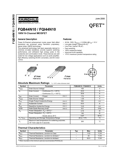
FQB44N10中文资料
Turn-On Delay Time
tr
Turn-On Rise Time
td(off)
Turn-Off Delay Time
tf
Turn-Off Fall Time
Qg
Total Gate Charge
Qgs
Gate-Source Charge
Qgd
Gate-Drain Charge
VDD = 50 V, ID = 43.5 A, RG = 25 Ω
10-1 0.2 0.4
25℃
※ Notes : 1. VGS = 0V 2. 250μs Pulse Test
0.6 0.8 1.0 1.2 1.4 1.6 1.8 2.0 V , Source-Drain Voltage [V]
-55 to +175
300
Units V A A A V mJ A mJ
V/ns W W
W/°C °C
°C
Thermal Characteristics
Symbol
Parameter
RθJC
Thermal Resistance, Junction-to-Case
RθJA
Thermal Resistance, Junction-to-Ambient *
4000 3500 3000 2500 2000 1500 1000 500
0 10-1
Ciss = Cgs + Cgd (Cds = shorted) Coss = Cds + Cgd Crss = Cgd
Ciss C
oss
C rss
※ Notes :
1. VGS = 0 V 2. f = 1 MHz
贴片电子元件代码(丝印)查询(带完整目录)

贴片电子元件代码(丝印)查询(带完整目录)THE SMDCODEBOOKSMD Codes.SMD devices are, by their very nature, too small to carry conventional semiconductor type numbers. Instead, a somewhat arbitrary coding system has grown up, wherethe device package carries a simple two- or three-character ID code.Identifying the manufacturers' type number of an SMD device fromthe package code can be a difficult task, involving combing throughmany different databooks.This HTML book is designed to provide an easy means of deviceidentification. It lists well over 3,400 device codes in alphabeticalorder, together with type numbers, device characteristics or equivalents and pinout information.How to use the SMD CodebookTo identify a particular SMD device, first identify the package style and note the ID code printed on the device. Now look up the code in the alphanumeric listing which forms the main partof this book by clicking on the first character shown in the left-menu.Unfortunately, each device code is not necessarily unique. For example a device coded 1A might be either a BC846A or a FMMT3904. Even the same manufacturer may use the same code for different devices!If there is more than one entry, use the package style to differentiate between devices with the same ID code. This compilation has been collected from R P Blackwell G4PMK, manufacturers' data and other sources of SMD device ID codes, pinout and leaded device equivalent information.The entries under the Manufacturer column are not intended to be comprehensive; rather they are intended to provide help on locating sources of more detailed information if you require it.ID Code VariationsMany manufacturers use an extra letter as their own identification code. If the device is from Philips it will sometimes have a lower case 'p' (or sometimes 't') added to the code; Siemens devices usually have a lower case 's'.For example, if the code is 1A, according to the table there are a number of possibilities:1A BC846A Phi ITT N BC546A1A FMMT3904 Zet N 2N39041A MMBT3904 Mot N 2N39041A IRLML2402 IR F n-ch mosfet 20V 0.9AThis has been a problem in the past, however recently manufacturers have been adding lower case letters which clarify the code.Many recent Motorola devices have a small superscript letterafter the device code, such as SA C . (This smaller letter is merely a month of manufacture code.)Many devices from Rohm Semiconductors which start with G have direct equivalents found in the rest of the number. For example GD1 is the same as D1 which is a BCW31.Some devices have a single coloured letter (usually on extremely small diode packages). Colour, if significant, is shown in small type after the code letter.An 'L' suffix usually indicates a low-profile package, such as an SOT323 orSC70.SOT323.SC70.Reverse joggle devices do present a few problems. They oftern have an 'R' in the type number. A reverse package is one where the lead have been bent up instead of down. So it's a mirror image of a conventional device. Identification is usually possible from the code number, but some manufacturers use the same code. In these cases, it's a case of looking at the device with a magnifying glass. The leads of most normal packages come out closer to the circuit board side of the device; conversely a reverse joggle package will have them coming out closer to the 'top' of the device.Sometimes a series of devices, derived from the same die,have related type (not code) numbers. Often an 'R' will indicate a reverse joggle package, and/or a 'W' indicate a smaller package variant, such as SOT343. Sometimes similarities are also found in the code numbers. For example:Recently some manufacturers have used a symbol or lower case letter to indicate the country of manufacture. These have been ignored in the alphabetical ordering. For example:'67' is the code for a BFP67 (SOT143 package) ,'67R' is the code for the reverse joggle variant BFP67R (SOT143R),'W67' is the code for a SOT343 package version.SOT143.'Z-S' and 'ZtS ' are both 2PC4081Q devices made by Philips; the first made in Hong Kong and the second in Malaysia; this appears in the codebook classified under ZS.Leaded equivalent device and informationWhere possible, the listing gives the part number of a conventional wire-leaded device with equivalent characteristics. If the leaded device is well-known then no more information is given. If the device is less common, some additional information will sometimes be given. Where no exact leaded equivalent exists, a brief device description is given, which may be sufficient to allow substitution with another device.When describing device characteristics, some terms are implied from the type of device. For example, a voltage specified for a rectifier diode is usually the maximum PIV (peak inverse voltage) of the diode, but for a zener diode the operating (zenervoltage) will be given.Normally, where a voltage, current or power is specified, these will be limiting values. For example, a device specified as NPN 20V 0.1A 1W is a NPN transistor with a Vce (max) of 20V, maximum collector current of 100mA and a maximum total power dissipation of 1W. Some of the transistors are types with integrated resistors; in the list, a base resistor means a resistor connected in series with the base. When two resistor values are given, the first is the series base resistor, and the second the resistor between base and emitter.Digital Transistors (dtr)These are transistors with built-in resistors.Some have one resistor between base and emitter, others in series with the base. Many others have both.To keep things simple, the series resistor is called R1 and the base emitter resistor is called R2. If both are present, then two values are given, R1 first. So 4k7 + 10k means that R1 (the base resistor) is 4k7 and R2 (the resistor between base and emitter) is 10k.ConclusionIdentifying the manufacturers' type number of an SMD device from the package code can be a difficult task, involving combing through many different databooks. This HTML book is designed to provide an easy means of device identification.Abbreviationsamp amplifieratten attenuatora anodeb basec cathodeca common anodecc common cathodecomp complementd draindg dual gatedtr digital transistor (see codebook introduction) enh enhancement (mode - FETs)fet field effect transistorfT transition frequencyGaAsfet Gallium Arsenide field effect transistorg gategnd groundgp general purposehfe small signal current gaini/p inputId drain currentIg gate currentIr reverse leakage current (diodes)jfet junction field effect transistorMAG maximum available gainmax maximummin minimummmic microwave minature integrated circuit modamp modular amplifier - an mmic amplifier mosfet metal oxide insulated gate fetn-ch n-channel fet (any type)npn npn bipolar transistoro/p outputp-ch p-channel fet (any type)pin pin diodepkg packagepnp pnp bipolar transistorprot protection, protected (as in mosfet gate) res resistors sourceser seriesSi siliconsubstr substratesw switch or switchingVce collector - emitter voltage (maximum) Vcc collector supply voltageManufacturer abbreviationsAgi Agilent (was HP)Fch FairchildHP Hewlett-Packard (Now Agilent)Inf Infineon (was Siemens)ITT ITT SemiconductorsMC Mini-CircuitsMot Motorola (now ON Semiconductors) Nat National SemiconductorNec NECNJRC New Japan Radio CoON ON Semiconductors (was Motorola) Phi PhilipsRoh RohmSGS SGS-ThompsonSie Siemens (now Infineon)Sil Siliconix (Vishay-Silliconix)Tem Temic SemiconductorsTfk Telefunken (Vishay-T elefunken)Tok Toko Inc.Zet ZetexCodes beginning with '0'Code Device Manufacturer Base Package Leaded Equivalent/Data0 2SC3603 Nec CX SOT173 Npn RF fT 7GHz005 SSTPAD5 Sil J - PAD-5 5pA leakage diodep01 PDTA143ET Phi N SOT23 pnp dtr 4k7+4k7t01 PDTA143ET Phi N SOT23 pnp dtr 4k7+4k701 Gali-1 MC AZ SOT89 DC-8GHz MMIC amp 12dB gain 010 SSTPAD10 Sil J - PAD-10 10pA leakage diode 011 SO2369R SGS R SOT23R 2N236902 BST82 Phi M - n-ch mosfet 80V 175mA02 MRF5711L Mot X SOT143 npn RF MRF57102 DTCC114T Roh N - 50V 100mA npn sw + 10k base res 02 Gali-2 MC AZ SOT89 DC-8GHz MMIC amp 16dB gain p02 PDTC143ET Phi N SOT23 npn 4k7+4k7 bias rest02 PDTC143ET Phi N SOT23 npn 4k7+4k7 bias res03 Gali-3 MC AZ SOT89 DC-3GHz MMIC amp 22dB gain 03 DTC143TE Roh N EMT3 npn dtr R1 4k7 50V 100mA03 DTC143TUA Roh N SC70 npn dtr R1 4k7 50V 100mA03 DTC143TKA Roh N SC59 npn dtr R1 4k7 50V 100mA04 DTC114TCA Roh N SOT23 npn dtr R1 10k 50V 100mA 04 DTC114TE Roh N EMT3 npn dtr R1 10k 50V 100mA 04 DTC114TUA Roh N SC70 npn dtr R1 10k 50V 100mA 04 DTC114TKA Roh N SC59 npn dtr R1 10k 50V 100mA 04 MRF5211L Mot X SOT143 pnp RF MRF52104 Gali-4 MC AZ SOT89 DC-4GHz MMIC amp 17.5 dBm -04PMSS3904 Phi N SOT323 2N3904t04 PMBS3904 Phi N SOT23 2N390405 Gali-4 MC AZ SOT89 DC-4GHz MMIC amp 18 dBm o/p 05 DTC124TE Roh N EMT3 npn dtr R1 22k 50V 100mA 05 DTC124TUA Roh N SC70 npn dtr R1 22k 50V 100mA 05 DTC124TKA Roh N SC59 npn dtr R1 22k 50V 100mA 05F TSDF1205R Tfk WQ - fT12GHz npn 4V 5mA06 Gali-6 MC AZ SOT89 DC-4GHz MMIC amp 115 dBm o/p 06 DTC144TE Roh N EMT3 npn dtr R1 47k 50V 100mA 06 DTC144TUA Roh N SC70 npn dtr R1 47k 50V 100mA 06 DTC144TKA Roh N SC59 npn dtr R1 47k 50V 100mA-06 PMSS3906 Phi N SOT323 2N3906t06 PMBS3906 Phi N SOT23 2N3906020 SSTPAD20 Sil J - PAD-20 20pA leakage diode 050 SSTPAD50 Sil J - PAD-50 50pA leakage diode 081 SO2369AR SGS R SOT23R 2N2369A09 DTC115TUA Roh N SC70 npn dtr R2 100k 50V 100mA 09 DTC115TKA Roh N SC59 npn dtr R2 100k 50V 100mA 0A MUN5111DW1 Mot DO SOT363 dual pnp dtr 10k+10k 0A DTC125TUA Roh N SC70 npn dtr R2 100k 50V 100mA0A DTC125TKA Roh N SC59 npn dtr R2 100k 50V 100mA0B MUN5112DW1 Mot DO SOT363 dual pnp dtr 22k+22k0C MUN5113DW1 Mot DO SOT363 dual pnp dtr 47k+47k0D MUN5114DW1 Mot DO SOT363 dual pnp dtr 10k+47k 0E MUN5115DW1 Mot DO SOT363 dual pnp dtr R1 10k0F MUN5116DW1 Mot DO SOT363 dual pnp dtr R1 4k70G MUN5130DW1 Mot DO SOT363 dual pnp dtr 1k0+1k0 0H MUN5131DW1 Mot DO SOT363 dual pnp dtr 2k2+2k2 0J MUN5132DW1 Mot DO SOT363 dual pnp dtr 4k7+4k70K MUN5133DW1 Mot DO SOT363 dual pnp dtr 4k7+47k0L MUN5134DW1 Mot DO SOT363 dual pnp dtr 22k+47k0M MUN5135DW1 Mot DO SOT363 dual pnp dtr 2k2+47k Codes beginning with '1'Code Device Manufacturer Base Package Leaded Equivalent/Data1 2SC3587 Nec CX - npn RF fT10GHz1 BA277 Phi I SOD523 VHF Tuner band switch diode1 (red) BB669 Sie I SOD323 56-2.7 pF varicap10 MRF9411L Mot X SOT143 npn Rf 8GHz MRF94110A PZM10NB2A Phi A SOT346 dual ca 10V 0.3W zener10V PZM10NB Phi C SOT346 10V 0.3W zener10Y BZV49-C10 Phi O SOT89 10V 1W zener11 MRF9511L Mot X SOT143 npn RF 8GHz MRF95111 MUN5311DW1 Mot DP SOT363 npn/pnp dtr 10k+10k11 PDTA114EU Phi N SOT416 pnp dtrp11 PDTA114TT Phi N SOT23 pnp dtrt11 PDTA114TT Phi N SOT23 pnp dtr11A PZM11NB2A Phi A SOT346 dual ca 11V 0.3W zener11A MMBD1501A Nat C SOT23 Si diode 200V 100mA11V PZM11NB Phi C SOT346 11V 0.3W zener11Y BZV49-C11 Phi O SOT89 11V 1W zener12 MUN5312DW1 Mot DP SOT363 npn/pnp dtr 22k+22k12 DTA123EUA Rho N SC70 pnp dtr 2k2+2k2 50V 100ma12 DTA123EKA Rho N SC59 pnp dtr 2k2+2k2 res 50V 100ma p12 PDTC114TT Phi N SOT23 npn dtrt12 PDTC114TT Phi N SOT23 npn dtr12A MMBD1502A Nat K SOT23 Si diode 200V 100mA12A PZM12NB2A Phi A SOT346 dual ca 12V 0.3W zener12E ZC2812E Zet D SOT23 dual series RF schottky15V 20mA 12V PZM12NB Phi C SOT346 12V 0.3W zener12Y BZV49-C12 Phi O SOT89 12V 1W zener13 DTA143EUA Rho N SC70 pnp dtr 4k7+4k7 50V 100ma13 DTA143EKA Rho N SC59 pnp dtr 4k7+4k7 50V 100ma13 DTA143ECA Rho N SOT23 pnp dtr 4k7+4k7 50V 100ma13t BC846BPN Phi N SOT363 BC546B13s BAS125 Sie C SOT23 Schottky sw 24V 100mA13s BAS125W Sie C SOT323 Schottky sw 24V 100mA13 MA4CS103A M/A C SOT23 Schottky RF 20V 100mA13 MUN5313DW1 Mot DP SOT363 npn/pnp dtr 47k+47k13A MMBD1503A Nat D SOT23 dual Si diode 200V 100mA 13A PZM13NB2A Phi A SOT346 dual ca 13V 0.3W zener 13E ZC2813E Zet A SOT23 dual ca RF schottky15V 20mA 13V PZM13NB Phi C SOT346 13V 0.3W zener13Y BZV49-C13 Phi O SOT89 13V 1W zener14s BAS125-04 Sie D SOT23 Dual series Schottky 25V 100mA 14s BAS125-04W Sie D SOT323 Dual series Schottky 25V 100mA 14 BAT114-099R Sie DQ - Quad Schottky crossover ring 14 DTA114EUA Roh N SC70 pnp dtr 10k + 10k14 DTA114EKA Roh N SC59 pnp dtr 10k + 10k14 MUN5314DW1 Mot DP SOT363 npn/pnp dtr 10k R114 DTA114ECA Roh N SOT23 pnp dtr 10k + 10k14A MMBD1504A Nat B - dual cc Si diode 200V 100mA 15s BAS125-05 Sie B SOT23 dual cc Schottky 25V 100mA 15s BAS125-05W Sie B SOT323 dual cc Schottky 25V 100mA 15 DTA124EUA Roh N SC70 pnp dtr 30V 50mA 22k+22k 15 DTA124EKA Roh N SC59 pnp dtr 30V 50mA 22k+22k 15 DTA124ECA Roh N SOT23 pnp dtr 30V 50mA 22k+22k 15 MUN5315DW1 Mot DP SOT363 npn/pnp dtr 10k R115 MMBT3960 Mot N - 2N396015A MMBD1505A Nat A - dual ca Si diode 200V 100mA 15APZM15NB2A Phi A SOT346 dual ca 15V 0.3W zener15V PZM15NB Phi C SOT346 15V 0.3W zener15Y BZV49-C15 Phi O SOT89 15V 1W zenerp16 PDTC114ET Phi N SOT23 npn dtrt16 PDTC114EU Phi N SOT323 npn dtr16s BAS125-06 Sie A SOT23 dual ca Schottky 25V 100mA 16s BAS125-06W Sie A SOT323 dual ca Schottky 25V 100mA 16 MUN5316DW1 Mot DP SOT363 npn/pnp dtr 4k7 R116 DTA144EUA Roh N SC70 pnp dtr 30V 50mA 47k+47k 16 DTA144EKA Roh N SC59 pnp dtr 30V 50mA 47k+47k 16V PZM16NB Phi C SOT346 16V 0.3W zener16Y BZV49-C16 Phi O SOT89 16V 1W zener17s BAS125-07 Sie S SOT143 dual Schottky 25V 100mA 17s BAS125-07W Sie S SOT343 dual Schottky 25V 100mA p17 PDTC124ET Phi N SOT23 npn dtrt17 PDTC124EU Phi N SOT323 npn dtr18 BFP181T Tfk X - npn Rf fT 7.8GHz 10V 20mA 18 PDTC143ZK Phi N SOT346 npn dtr 4k7+47kp18 PDTC143ZT Phi N SOT23 npn dtr 4k7+47kt18 PDTC143ZT Phi N SOT23 npn dtr 4k7+47k18V PZM18NB Phi C SOT346 18V 0.3W zener18Y BZV49-C18 Phi O SOT89 18V 1W zener19 PDTA143ZK Phi N SOT346 pnp dtr 4k7+47k19 DTA115EUA Rho N SC70 pnp dtr 100k+100k 50V 100ma 19 DTA115EKA Rho N SC59 pnp dtr 100k+100k 50V 100ma p19 PDTA143ZT Phi N SOT23 pnp dtr 4k7+47kt19 PDTA143ZT Phi N SOT23 pnp dtr 4k7+47k100 SSTPAD100 Sil J SOT23 PAD-100 100pA leakage diode 101 PZM10NB1 Phi C SOT346 10V 0.3W zener102 PZM10NB2 Phi C SOT346 10V 0.3W zener103 PZM10NB3 Phi C SOT346 10V 0.3W zener111 PZM11NB1 Phi C SOT346 11V 0.3W zener111 DTA113ZUA Roh N SC70 pnp dtr 1k+10k 50V 100mA 112 PZM11NB2 Phi C SOT346 11V 0.3W zener113 PZM11NB3 Phi C SOT346 11V 0.3W zener113 DTA143ZUA Roh N SC70 pnp dtr 4k7+47k 50V 100mA 121 PZM12NB1 Phi C SOT346 12V 0.3W zener121 DTC113ZUA Roh N SC70 npn dtr 1k+10k 50V 100mA 122 PZM12NB2 Phi C SOT346 12V 0.3W zener123 PZM12NB3 Phi C SOT346 12V 0.3W zener123 DTC143ZUA Roh N SC70 npn dtr 4k7+47k 50V 100mA 131 PZM13NB1 Phi C SOT346 13V 0.3W zener132 PZM13NB2 Phi C SOT346 13V 0.3W zener132 DTA123JUA Roh N SC70 pnp dtr 2k2+47k 50V 100mA 133 PZM13NB3 Phi C SOT346 13V 0.3W zener142 DTA123JUA Roh N SC70 npn dtr 2k2+47k 50V 100mA 151 PZM15NB1 Phi C SOT346 15V 0.3W zener152 PZM15NB2 Phi C SOT346 15V 0.3W zener153 PZM15NB3 Phi C SOT346 15V 0.3W zener156 DTA144VUA Roh N SC70 pnp dtr 47k+10k 50V 100mA 161 PZM16NB1 Phi C SOT346 16V 0.3W zener162 PZM16NB2 Phi C SOT346 16V 0.3W zener163 PZM16NB3 Phi C SOT346 16V 0.3W zener166 DTC144VUA Roh N SC70 npn dtr 47k+10k 50V 100mA 179 FMMT5179 Zet N - 2N5179181 PZM18NB1 Phi C SOT346 18V 0.3W zener182 PZM18NB2 Phi C SOT346 18V 0.3W zener183 PZM18NB3 Phi C SOT346 18V 0.3W zener1A BC846A Phi N SOT23 BC546A1A BC846AT Phi N SOT416 BC546A1Ap BC846A Phi N SOT23 BC546A1At BC846A Phi N SOT23 BC546A1At BC846AW Phi N SOT323 BC546A1A- BC846AW Phi N SOT323 BC546A1A FMMT3904 Zet N SOT23 2N39041A MMBT3904 Mot N SOT23 2N39041A IRLML2402 IR F SOT23 n-ch mosfet 20V 0.9Ap1A PMMT3904 Phi N SOT23 2N3904p1A PXT3904 Phi N SOT89 2N3904t1A PMMT3904 Phi N SOT23 2N3904t1A PMST3904 Phi N SOT323 2N3904-1A PMST3904 Phi N SOT323 2N39041AM MMBT3904L Mot N SOT23 2N39041B BC846B Phi N SOT23 BC546B1B BC846BT Phi N SOT416 BC546B1Bp BC846B Phi N SOT23 BC546B1Bt BC846B Phi N SOT23 BC546B1Bt BC846BW Phi N SOT323 BC546B1B- BC846BW Phi N SOT323 BC546B1B FMMT2222 Zet N SOT23 2N22221B MMBT2222 Mot N SOT23 2N22221B IRLML2803 IR F SOT23 n-ch mosfet 30V 0.9Ap1B PMBT2222 Phi N SOT23 2N2222t1B PMBT2222 Phi N SOT23 2N2222t1B PMST2222 Phi N SOT233 2N2222-1B PMST2222 Phi N SOT323 2N22221Bs BC817UPN Sie N SC74 -1Cp BAP50-05 Phi B SOT23 dual cc GP RF pin diode 1C FMMT-A20 Zet N SOT23 MPSA201C MMBTA20L Mot N SOT23 MPS39041C IRLML6302 IR F SOT23 p-ch mosfet 20V 0.6A1Cs BC847S Sie - SOT363 BC4571Dp BC846 Phi N SOT23 BC4561Dt BC846 Phi N SOT23 BC4561Dt BC846W Phi N SOT323 BC4561D- BC846W Phi N SOT323 BC4561D MMBTA42 Mot N SOT23 MPSA42 300V npn1D IRLML5103 IR F SOT23 p-ch mosfet 30V 0.6Ap1D PMBTA42 Phi N SOT23 MPSA42 300V npnp1D PXTA42 Phi N SOT89 MPSA42 300V npnt1D PMBTA42 Phi N SOT23 MPSA42 300V npnt1D PMSTA42 Phi N SOT323 MPSA42 300V npn1Ds BC846U Sie N SC74 BC4561Ds BC846U Sie - SOT363 BC4561DN 2SC4083 Roh N - npn 11V 3.2GHz TV tuners 1DR MSD1328R Mot N SOT346 npn gp 25V 500mA1E BC847A Phi N SOT23 BC547A1E BC847AT Phi N SOT416 BC547A1Ep BC847A Phi N SOT23 BC547A1Et BC847A Phi N SOT23 BC547A1Et BC847A Phi N SOT323 BC547A1E- BC847A Phi N SOT323 BC547A1ER BC847AR Phi R SOT23R BC547A1E FMMT-A43 Zet N - MPSA431E MMBTA43 Mot N SOT23 MPSA43 200V npnt1E PMBTA43 Mot N SOT23 MPSA43 200V npnt1E PMSTA43 Mot N SOT323 MPSA43 200V npn1Es BC847A Sie N SOT23 BC4571Es BC847AW Sie N SOT323 BC4571EN 2SC4084 Roh N - npn 20V 2.0GHz TV tuners 1F BC847BPhi N SOT23 BC547B1F BC847BT Phi N SOT416 BC547B1Fs BC847B Sie N SOT23 BC547B1Fs BC847BT Sie N SC75 BC547B1Fs BC847BW Sie N SOT323 BC547B1Fp BC847B Phi N SOT23 BC547B1Ft BC847B Phi N SOT23 BC547B1Ft BC847BW Phi N SOT323 BC547B1F- BC847BW Phi N SOT323 BC547B1FR BC847BR Phi R SOT23R BC547B1F MMBT5550 Mot N SOT23 2N5550 140V npn p1F PMBT5550 Phi N SOT23 2N5550 140V npn t1F PMBT5550 Phi N SOT23 2N5550 140V npnt1F PMST5550 Phi N SOT323 2N5550 140V npn 1FZ FMBT5550 Zet N SOT23 2N5550 140V npn 1G BC847C Phi N SOT23 BC547C1G BC847CT Phi N SOT416 BC547C1Gp BC847C Phi N SOT23 BC547C1Gt BC847CW Phi N SOT323 BC547C1G- BC847CW Phi N SOT323 BC547C1Gs BC847C Sie N SOT23 BC547C1Gs BC847CW Sie N SOT323 BC547C1GR BC847CR Phi R SOT23R BC547C1GT SOA06 SGS N SOT23 MPSA061G FMMT-A06 Zet N SOT23 MPSA061G MMBTA06 Mot N SOT23 MPSA06p1G PMMTA06 Phi N SOT23 MPSA06t1G PMMTA06 Phi N SOT23 MPSA06t1G PMMTA06 Phi N SOT323 MPSA061GM MMBTA06 Mot N SOT23 MPSA061Hp BC847 Phi N SOT23 BC5471Ht BC847 Phi N SOT23 BC5471Ht BC847W Phi N SOT323 BC5471H- BC847W Phi N SOT323 BC5471H FMMT-A05 Zet N - MPSA051H MMBTA05 Mot N SOT23 MPSA05t1H MMBTA05 Phi N SOT323 MPSA051HT SOA05 SGS N SOT23 MPSA051J BC848A Phi N SOT23 BC548A1Js BC848A Sie N SOT23 BC548A1Js BC848AW Sie N SOT323 BC548A1J FMMT2369 Zet N SOT23 2N23691J MMBT2369 Mot N SOT23 MPS23691Js BCV61A Sie VQ SOT143 npn current mirror hFe 180 1Jp BCV61A Phi VQ SOT143 npn current mirror hFe 180 p1J PMBT2369 Phi N SOT23 2N2369t1J PMBT2369 Phi N SOT23 2N2369t1J PMBT2369 Phi N SOT323 2N23691JA MMBT2369A Mot N SOT23 MPS2369A1JR BC848AR Phi R SOT23R BC548A1JZ BC848A Zet N SOT23 BC548A1K BC848B ITT N SOT23 BC548B1Kp BC848B Phi N SOT23 BC548B1Ks BC848B Sie N SOT23 BC548B1Ks BC848BW Sie N SOT323 BC548B1K MMBT6428 Mot N SOT23 MPSA18 50Vp1K PMBT6428 Phi N SOT23 MPSA18 50Vt1K PMBT6428 Phi N SOT23 MPSA18 50Vt1K PMBT6428 Phi N SOT323 MPSA18 50V1K FMMT4400 Zet N SOT23 2N44001Ks BCV61B Sie VQ SOT143B npn current mirror hFe 290 1Kp BCV61B Phi VQ SOT143B npn current mirror hFe 290 1KR BC848BR Phi R SOT23R BC548B1KM MMBT6428L Mot N SOT23 MPSA18 50V1KZ FMMT4400 Zet N SOT23 2N44001L BC848C ITT N SOT23 BC548C1Lp BC848C Phi N SOT23 BC548C1Ls BC848C Sie N SOT23 BC548C1Ls BC848CW Sie N SOT323 BC548C1L MMBT6429 Mot N - MPSA18 45V1L FMMT4401 Zet N - 2N44011L BCV61C Sie VQ SOT143B npn current mirror hFe 520 1Lp BCV61C Phi VQ SOT143B npn current mirror hFe 520 p1L PMBT6429 Phi N SOT23 MPSA18 45Vt1L PMBT6429 Phi N SOT23 MPSA18 45Vt1L PMBT6429 Phi N SOT323 MPSA18 45V1LR BC848CR Phi R SOT23R BC548C1Mp BC848 Phi N SOT23 BC5481M MMBTA13 Mot N SOT23 MPSA13 darlington1Mp BCV61 Phi VQ SOT143B npn current mirror1M FMMT-A13 Zet N SOT23 MPSA13p1M PXTA13 Phi N SOT89 MPSA13 darlingtonp1M PMBTA13 Phi N SOT23 MPSA13 darlingtont1M PMBTA13 Phi N SOT23 MPSA13 darlington1N FMMT-A14 Zet N SOT23 MPSA141N MMBTA14 Mot N SOT23 MPSA14 darlington1N5 ZTX11N15DF Zet N SOT23 npn 15V 3A low saturation V p1N PMBTA14 Mot N SOT23 MPSA14 darlingtonp1N PXTA14 Mot N SOT89 MPSA14 darlingtont1N PMBTA14 Mot N SOT23 MPSA14 darlington1P FMMT2222A Zet N - 2N2222A1P MMBT2222A Mot N SOT23 2N2222A1P BC847PN Sie DI - pnp/npn separate pair gp AF p1P PMBT2222A Phi N SOT23 2N2222Ap1P PXT2222A Phi N SOT89 2N2222At1P PMBT2222A Phi N SOT23 2N2222At1P PMST2222A Phi N SOT323 2N2222A1Q MMBT5088 Mot N SOT23 MPSA18 Vce 30Vp1Q PMBT5088 Phi N SOT23 MPSA18 Vce 30Vt1Q PMBT5088 Phi N SOT23 MPSA18 Vce 30Vt1Q PMST5088 Phi N SOT323 MPSA18 Vce 30V1R MMBT5089 Mot N SOT23 MPSA18 Vce 25Vt1R PMST5089 Phi N SOT323 MPSA18 Vce 25V1S MMBT2369A Nat N SOT23 2N2369A 500MHz sw npn 1S MSC3130 Mot H SOT346 npn RF fT 1.4GHz 10V1T MMBT3960A Mot N - 2N3960A1U MMBT2484L Mot N SOT23 MPSA181V MMBT6427 Mot H SOT23 2N6426/7 darlington npn 1Vp BF820 Phi N SOT23 npn 300V 50mA BF4201Vt BF820 Phi N SOT23 npn 300V 50mA BF4201Vt BF820W Phi N SOT323 npn 300V 50mA BF4201V- BF820W Phi N SOT323 npn 300V 50mA BF4201W FMMT3903 Zet N SOT23 2N39031Wp BF821 Phi N SOT23 pnp 300V 50mA BF421 1Wt BF821 Phi N SOT23 pnp 300V 50mA BF4211W t BF822W Phi N SOT323 pnp 300V 50mA BF4211W - BF822W Phi N SOT323 pnp 300V 50mA BF421 1X MMBT930L Mot N SOT23 MPS39041Xp BF822 Phi N SOT23 npn 250V 50mA BF422 1Xt BF822 Phi N SOT23 npn 250V 50mA BF422 1Y MMBT3903 Mot N SOT232N39031Yp BF823 Phi N SOT23 pnp 250V 50mA BF423 1Yt BF823 Phi N SOT23 pnp 250V 50mA BF423 1Z BAS70-06 Zet A SOT23 dual RF CA schottky diode 1Z MMBT6517 Mot N SOT23 2N6517 npn Vce 350VCodes beginning with '2'Code Device Manufacturer Base Package Leaded Equivalent/Data2 BAT62-02W Sie I SCD80 BAT16 schottky diode2 (blue) BAR64-03W Sie I SOD323 pin diode2 2SC3604 Nec CX - npn RF fT8GHz 12dB@2GHz 2 (white) BB439 Sie I SOD323 29-5 pF varicap20 MRF5811 Mot X SOT143 npn Rf fT 5GHz 0.2A-20 PDTC114WU Phi N SOT323 npn dtr20F TSDF1220 Tfk X SOT143 fT 12GHz npn 6V 20mA 20V PZM20NB Phi C SOT346 20V 300mW zener 20Y BZV49-C20 Phi O SOT89 20V 1W zener21 Gali-21 MC AZ SOT89 DC-8GHz MMIC amp 14 dB gain22 MMBT4209 Nat N SOT23 pnp sw 850MHz 2N420922 DTC123EUA Rho N SC70 npn dtr 2k2+2k2 50V 100ma22 DTC123EKA Rho N SC59 npn dtr 2k2+2k2 50V 100ma22V PZM22NB Phi C SOT346 22V 300mW zener 22Y BZV49-C22 Phi O SOT89 22V 1W zener23 MMBT3646 Nat N SOT23 npn sw 350MHz 2N364623 DTC143EUA Roh N SC70 pnp dtr 50V 100mA 4k7+ 4k723 DTC143EKA Roh N SC59 pnp dtr 50V 100mA 4k7+ 4k7-23 PDTA114TU Phi N SOT323 pnp dtr R1 10k t23 PDTA114TU Phi N SOT323 pnp dtr R1 10k24 MMBD2101 Nat C SOT23 Si diode 100V 200mA24 DTC114ECA Roh N SOT23 npn dtr 50V 100mA 10k + 10k24 DTC114EUA Roh N SC70 npn dtr 50V 100mA 10k + 10k24 DTC114EKA Roh N SC59 npn dtr 50V 100mA 10k + 10k24 2SC5006 Nec N - npn RF fT 4.5GHz @3V 7mA-24 PDTC114TU Phi N SOT323 npn dtr R1 10k t24 PDTC114TU Phi N SOT323 npn dtr R1 10k 24V PZM24NB Phi C SOT346 24V 300mW Zener 24Y BZV49-C24 Phi O SOT89 24V 1W zener25 MMBD2102 Nat K SOT23 Si diode 100V 200mA25 DTC124ECA Roh N SOT23 npn dtr 50V 100mA 22k + 22k25 DTC124EKA Roh N SC59 npn dtr 50V 100mA 22k + 22k25 DTC124EUA Roh N SC70 npn dtr 50V 100mA 22k + 22k26 MMBD2103 Nat D SOT23 dual MMBD120126 DTC144EKA Roh N SC59 npn dtr 50V 30mA 47k + 47k26 DTC144EUA Roh N SC70 npn dtr 50V 30mA 47k + 47k27 MMBD2104 Nat B SOT23 dual cc MMBD120127V PZM27NB Phi C SOT346 27V 300mW Zener 27Y BZV49-C27 Phi O SOT89 27V 1W zener28 BFP280T Tfk W - npn RF fT 7GHz 8V 10mA28 MMBD2105 Nat A SOT23 dual ca MMBD1201-28 PDTA114WU Phi N SOT323 pnp dtr29 MMBD1401 Nat C SOT23 Si diode 200V 100mA29 DTC115EE Roh N EMT3 npn dtr 100k +100k 50V 20mA29 DTC115EUA Roh N SC70 npn dtr 100k +100k 50V 20mA29 DTC115EKA Roh N SC59 npn dtr 100k +100k 50V 20mA200 SSTPAD200 Sil J - PAD-200 200pA leakage diode 201 PZM20NB1 Phi C SOT346 20V 300mW Zener202 PZM20NB2 Phi C SOT346 20V 300mW Zener 203 PZM20NB3 Phi C SOT346 20V 300mW Zener 221 PZM22NB1 PhiC SOT346 22V 300mW Zener 222 PZM22NB2 Phi C SOT346 22V 300mW Zener 223 PZM22NB3 Phi C SOT346 22V 300mW Zener 241 PZM24NB Phi C SOT346 24V 300mW Zener 242 PZM24NB Phi C SOT346 24V 300mW Zener 243 PZM20NB Phi C SOT346 24V 300mW Zener 271 PZM2.7NB1 Phi C SOT346 2.7V 300mW Zener 272 PZM2.7NB2 Phi C SOT346 2.7V 300mW Zener 2A MMBT3906L Mot N SOT23 2N39062A MMBT3906W Mot N SOT323 2N39062A FMMT3906 Zet N SOT23 2N3906t2A PMBT3906 Phi N SOT23 2N3906t2A PMST3906 Phi N SOT323 2N3906p2A PMBT3906 Phi N SOT23 2N3906p2A PXT3906 Phi O SOT89 2N39062A4 PZM2.4NB2A Phi A SOT346 dual 2.4V cc Zener2A7 PZM2.7NB2A Phi A SOT346 dual 2.7V cc Zener2B BC849B ITT N SOT23 BC549B2Bs BC849B Sie N SOT23 BC549B2Bs BC849BW Sie N SOT323 BC549B2Bp BC849B Phi N SOT23 BC549B2Bt BC849BW Phi N SOT323 BC549B2B- BC849BW Phi N SOT323 BC549B2B FMMT2907 Zet N SOT23 2N29072B MMBT2907 Mot N SOT23 MPS2907p2B PMBT2907 Phi N SOT23 2N2907t2B PMBT2907 Phi N SOT23 2N29072BR BC849BR Phi R SOT23R BC549B2BZ FMMT2907 Zet N SOT23 2N29072C BC849C ITT N SOT23 BC549C2Cs BC849C Sie N SOT23 BC549C2Cs BC849CW Sie N SOT323 BC549C2Ct BC849C Phi N SOT23 BC549C2Ct BC849CW Phi N SOT323 BC549C2C- BC849CW Phi N SOT323 BC549C2C MMBTA70 Mot N SOT23 MPSA702CR BC849CR Phi R SOT23R BC549C2CZ FMMTA70 Zet N SOT23 MPSA702D MMBTA92 Mot N SOT23 MPSA92 pnp Vce 300V p2D PMBTA92 Phi N SOT23 MPSA92 pnp Vce 300V p2D PXTA92 Phi O SOT89 MPSA92 pnp Vce 300V t2D PMBTA92 Phi N SOT23 MPSA92 pnp Vce 300V t2D PMSTA92 Phi N SOT323 MPSA92 pnp Vce 300V 2E MMBTA93 Mot N SOT23 MPSA93 pnp Vce 200V 2E FMMT-A93 Zet N SOT23 MPSA93t2E PMBTA93 Phi N SOT23 MPSA93 pnp Vce 200V t2E PMSTA93 Phi N SOT323 MPSA93 pnp Vce 200V 2F BC850B ITT N SOT23 BC550B2Fs BC850B Sie N SOT23 BC550B2Fs BC850BW Sie N SOT323 BC550B2Fp BC850B Phi N SOT23 BC550B2Ft BC850B Phi N SOT23 BC550B2Ft BC850BW Phi N SOT323 BC550B2F- BC850BW Phi N SOT323 BC550B2F FMMT2907A Zet N SOT23 2N2907A2F MMBT2907A Mot N SOT23 MPS2907A2F MMBT2907AW Mot N SOT323 MPS2907Ap2F PMBT2907A Phi N SOT23 2N2907Ap2F PXT2907A Phi O SOT89 2N2907At2F PMBT2907A Phi N SOT23 2N2907At2F PMBT2907A Phi N SOT323 2N2907A2FR BC850BR Phi R SOT23R BC550B。
1N4148.1N4448
We reserve the right to make changes to improve technical design and may do so without further notice. Parameters can vary in different applications. All operating parameters must be validated for each customer application by the customer. Should the buyer use Vishay-Telefunken products for any unintended or unauthorized application, the buyer shall indemnify Vishay-Telefunken against all claims, costs, damages, and expenses, arising out of, directly or indirectly, any claim of personal damage, injury or death associated with such unintended or unauthorized use. Vishay Semiconductor GmbH, P.O.B. 3535, D-74025 Heilbronn, Germany Telephone: 49 ( 0 ) 7131 67 2831, Fax number: 49 ( 0 ) 7131 67 2423
Reverse current
Breakdown voltage Diode capacitance Rectification efficiency Reverse recovery time y
547B资料

MCC
VBE(on) @ VCE = 10 V
VCE(sat) @ IC/IB = 10 0.2 0.3 0.5 0.7 1.0 2.0 3.0 5.0 7.0 10 20 30 IC, COLLECTOR CURRENT (mAdc) 50 70 100
Figure 1. Normalized DC Current Gain
OFF CHARACTERISTICS
Collector–Emitter Breakdown Voltage (IC = 1.0 mA, IB = 0) Collector–Base Breakdown Voltage (IC = 100 µAdc) Emitter–Base Breakdown Voltage (IE = 10 mA, IC = 0)
V(BR)CBO
V
V(BR)EBO
V
ON CHARACTERISTICS
DC Current Gain (IC = 10 µA, VCE = 5.0 V) hFE BC547A/548A BC546B/547B/548B BC548C BC546 BC547 BC548 BC547A/548A BC546B/547B/548B BC547C/BC548C BC547A/548A BC546B/547B/548B BC548C VCE(sat) — VBE(sat) VBE(on) 0.55 — — — 0.7 0.77 — — — — 110 110 110 110 200 420 — — — 90 150 270 — — — 180 290 520 120 180 300 --— — — — 450 800 800 220 450 800 — — — V 0.3 1.0 V V —