MS-EXAFS 研究闪锌矿构型的GaP、GaAs 和GaSb半导体的结构
第二章 EXAFS谱学原理
X射线吸收精细结构(x-ray absorption fine structure,简写为XAFS)谱分为X射线吸收近边结构(x-ray absorption near edge structure,简写为XANES)谱和扩展X射线吸收精细结构(extend x-ray absorption fine structure)谱。
由于历史发展的原因和数据处理方法的不同,我们将这两种不同的谱学方法分开讨论,虽然现在我们意识到产生这两种振荡的原因实质上是一致的,即起源于被X射线激发出来的吸收原子内壳层电子(称光电子)的散射效应。
在介绍EXAFS方法之前,我们不妨先简单回顾一下EXAFS和XANES的发展历程,这对于我们理解这一独特实验方法大有好处。
§1. XAFS的发展历史和特点Frickle和Hertz在1920 年首次从实验上观察到XAFS现象,完整的XAFS 谱则由Ray和Kievet等在1929年测量到。
虽然人们很早就观察到XAFS现象,但是对其本质的认识却进展缓慢,经历了漫长的50余年时间。
历史上,很长一段时间内,存在着长程有序(long-range order, 缩写为LRO)理论和短程有序理论(short-range order, SRO)之争。
这是由于吸收边前后不长的1千多电子伏特范围内的不同能量段的精细结构的产生机制略有不同,又由于当时的实验能力不强,做一次实验需要花费一周左右的时间,故进展缓慢。
第一个对吸收边精细结构进行解释的是Kossel于1920年作出的,它指出这些峰是由激发的光电子跃迁到一系列外层未占据轨道造成的。
就现在的观点看来,Kossel理论基本上可以解释XAFS曲线的吸收边前和附近的结构,但是不能解释广延部分和近边部分(吸收边和广延部分之间的几十电子伏特的区域)的结构。
Kronig在1931年第一次利用量子力学观点解释固体物质产生的EXAFS,他认为这是因布里源区边界上的能隙产生的,这是由固体中的排列周期性,即长程有序决定的,这一理论后来被称之为长程有序理论。
闪锌矿结构半导体声子谱研究

闪锌矿结构半导体声子谱研究
杨炜栋;资剑;张开明
【期刊名称】《半导体学报:英文版》
【年(卷),期】1993(14)10
【摘要】我们采用两参数的Keating模型描述晶体的短程相互作用,并引入有效电荷Z描述长程的库仑相互作用,研究了极性半导体的晶格动力学性质。
对
SiC,GaAs,GaSb和InSb的计算表明,本文的结果与实验及其它理论计算符合较好。
由于本文的模型只引入了三个参数,具有参数少,物理图象清晰的性质,因此,这个模型可以应用到复杂的体系,如超晶格等。
【总页数】6页(P591-596)
【关键词】半导体;晶体;声子谱;闪锌矿;结构
【作者】杨炜栋;资剑;张开明
【作者单位】复旦大学物理系
【正文语种】中文
【中图分类】O471.4
【相关文献】
1.Cr掺杂闪锌矿AlP半导体的电子结构及磁性研究 [J], 周清;邓清梅;;;
2.Cr掺杂闪锌矿AlP半导体的电子结构及磁性研究 [J], 周清;邓清梅
3.用光谱、声子谱和EPR谱确定MgO:Ni2+的局域结构 [J], 谢林华;胡萍;黄平;丘岷
4.闪锌矿GaN/Ga_xIn_(1-x)N应变异质结中电子-光学声子散射率 [J], 李永治;班士良
5.闪锌矿结构Zn_(1-x)Mn_xSe混晶光学声子行为 [J], 过毅乐;劳浦东
因版权原因,仅展示原文概要,查看原文内容请购买。
半导体物理复习归纳

半导体物理复习归纳————————————————————————————————作者: ————————————————————————————————日期:一、半导体的电子状态1、金刚石结构(Si、Ge)Si、Ge原子组成,正四面体结构,由两个面心立方沿空间对角线互相平移1/4个空间对角线长度套构而成。
由相同原子构成的复式格子。
2、闪锌矿结构(GaAs)3-5族化合物分子构成,与金刚石结构类似,由两类原子各自形成的面心立方沿空间对角线相互平移1/4个空间对角线长度套构而成。
由共价键结合,有一定离子键。
由不同原子构成的复式格子。
3、纤锌矿结构(ZnS)与闪锌矿结构类似,以正四面体结构为基础,具有六方对称性,由两类原子各自组成的六方排列的双原子层堆积而成。
是共价化合物,但具有离子性,且离子性占优。
4、氯化钠结构(NaCl)沿棱方向平移1/2,形成的复式格子。
5、原子能级与晶体能带原子组成晶体时,由于原子间距非常小,于是电子可以在整个晶体中做共有化运动,导致能级劈裂形成能带。
6、脱离共价键所需的最低能量就是禁带宽度。
价带上的电子激发为准自由电子,即价带电子激发为导带电子的过程,称为本征激发。
7、有效质量的意义a.有效质量概括了半导体内部势场的作用(有效质量为负说明晶格对粒子做负功)b.有效质量可以直接由实验测定c.有效质量与能量函数对于k的二次微商成反比。
能带越窄,二次微商越小,有效质量越大。
8、测量有效质量的方法回旋共振。
当交变电磁场角频率等于回旋频率时,就可以发生共振吸收。
测出共振吸收时电磁波的角频率和磁感应强度,就可以算出有效质量。
为能观测出明显的共振吸收峰,要求样品纯度较高,且实验要在低温下进行。
9、空穴价带中空着的状态被看成带正电的粒子,称为空穴。
这是一种假想的粒子,其带正电荷+q,而且具有正的有效质量m p*。
10、轻/重空穴重空穴:有效质量较大的空穴轻空穴:有效质量较小的空穴11、间接带隙半导体导带底和价带顶处于不同k值的半导体。
掺镧钨酸铅晶体的EXAFS研究①
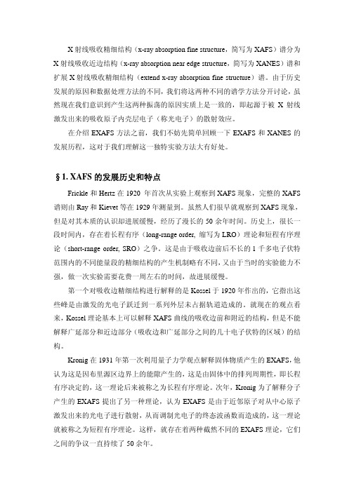
20卷3期结构化学(JIEGOU HUAXUE) V ol.20, No.3 2001.5 Chinese J. Struct. Chem. 214~216 掺镧钨酸铅晶体的EXAFS研究①林奇生a冯锡淇a满振勇a戚泽民b施潮淑 b(a中国科学院上海硅酸盐研究所无机功能材料开放实验室,上海,200050b中国科学技术大学国家同步辐射实验室,合肥,230039)利用EXAFS对固相合成的PbWO4多晶的W原子的近边结构进行研究,结果表明PWO 晶体掺镧15% m/o后,其第一配位层的配位数增加,同时WO键长变短,说明晶体中存在间隙氧离子。
最后,讨论了间隙氧离子的结构起因以及其在发光机制方面的作用。
关键词:钨酸铅闪烁晶体,掺杂,EXAFS钨酸铅(PbWO4, 以下简称PWO)是应用于欧洲核子研究中心(CERN)正在建设的大型强子对撞机LHC中的闪烁晶体材料[1~3]。
基于这一背景,自1994年以来,PWO成为各国竞相研究的热点。
此外,PWO在光电子和快离子导体方面也具有相当的潜力[4,5]。
许多研究表明,PWO具有结构敏感特征,晶体中的缺陷和杂质等对它的闪烁性能影响极大。
作为系列工作的一部分,我们对PWO作为基质的稀土掺杂进行了微结构研究,以确定晶体中可能存在的缺陷态,从而为了解晶体的发光机制、辐照损伤机理等提供依据。
1 实验原料PbO(5N)、WO3(5N)和La2O3(4N)粉末按(1-x):1:x的比例配成含La3+为15% m/o(摩尔百分比)的混合物,经800℃预烧,压片,在1100℃经固相反应2h,然后自然冷却得到无色多晶体。
经X射线粉末衍射(XRD)分析表明,见图1,产物可用Scheelite型PWO的晶胞参数进行指标化,说明稀土在这样的比例下的掺杂没有引起PWO的Scheelite型结构的根本改变。
考虑到Pb和W对X射线的强烈吸收,可能掩盖其它少量杂质(如过量的La2O3)的吸收。
GaAs

•
两种类型的杂质,即不管是浅能级杂质还是深能级杂质,通过与砷原子或镓原子的复杂结合而存在于砷 化镓晶体中。硅就是目前得到最广泛研究的一种掺杂剂,这种四族元素,在低温下与砷化镓作用,可形 成p型材料,在高温下与砷化镓作用,可形成n型材料。铬在砷化镓中是深受主原子,它的杂质能级接近 禁带中心位置,利用这一特点,可以在浅n型砷化镓材料中通过掺铬进行补偿而得到半绝缘材料。其它 的元素,如铜、氧、硒、碲、锡等在砷化镓中的行为也得到了广泛的研究,这样,我们可根据器件设计 的需求进行掺杂得到n型或p型砷化镓。
性能好,更适合空间能源领域;
温度系数小:能在较高的温度下正常工作。
GaAs太阳电池的特点——缺点
资源稀缺,价格昂贵,约Si材料的10倍;
污染环境,砷化物有毒物质,对环境会造成污染;
机械强度较分解,而且砷材料是一种易挥发性物质,在其制备过程中,要保证 严格的化学计量比是一件困难的事。
二、砷化镓晶体结构
• 砷化镓晶格是由两个面心立方(fcc)的子晶格(格点上分别是砷和镓的两个子晶格)沿空间体对角线 位移1/4套构而成。这种晶体结构在物理学上称之为闪锌矿结构。图1给出了砷化镓晶胞结构的示意 图,表1给出了在室温下目前已知砷化镓半导体材料的物理、电学参数。关于砷化镓的化学组成形 式,III-V族化合物共价键模型认为[2]:这类化合物形成四面体共价结合,成键时III族原子提供3个
• 砷化镓晶胞示意图(闪锌矿结构)
砷原子
镓原子
三、砷化镓能带结构
• 当在绝对零度以上温度时,一些电子因热能量而振动幅度加剧,如果其处于价带顶,所受的热能量
Q>=Ef时,就有可能脱离价带,跃迁进入导带,从而能在晶体中移动导电。在一块纯净的半导体中,电
扩展X射线吸收精细结构(EXAFS)谱
扩展X射线吸收精细结构(EXAFS)谱
• 10.2 XAFS理论:
• XAFS函数 • 首先,XAFS函数定义如下: E 0 E E 0 E • 其中 0(E)为单原子吸收系数;假设l0,m0是初态的角量子数和 磁量子数,在末态,出射波lm>受到近邻原子的散射而形成入 射波l‘m’> ,其散射振幅为Zl‘m’ ,lm,在单散射近似下,多 散射体的效应被简单地看成单散射效应的叠加,因此,XAFS函 数可以表示为: i j 2 Re P Z P e
扩展X射线吸收精细结构(EXAFS)谱
• 10.1 XAFS 原理: • 技术的特点 • (3)XAFS的敏感性。利用高强度的同步辐射光源及荧光XAFS技术, 可以测定样品中含量很低的元素的近邻结构.因而很适用于掺杂物 质中,杂质原子的近邻环境研究。 • (4)XAFS的取向性.利用偏振的X射线源并考虑多重散射效应,可 以研究样品中原子的配位键角及原子排列的空间取向。在某些情况 下,能够获得远配位层的原子结构信息或配位键角信息。
扩展X射线吸收精细结构(EXAFS)谱
• 10.2 XAFS理论:
• 吸收系数: • 本节主要介绍XAFS谱的基本理论,有关XAFS的论著可参阅文 献。 • 物质对x射线的吸收是一个光电过程。当吸收原子的壳层电子 受到x射线的激发,该x射线光子将其全部的能量转移给电子, 使光电子由初态i跃迁到受激后的末态f ,跃迁几率由 费米的黄金规则(Fermi‘s Golden Rule)给出: • • (11—1) 2 2
扩展X射线吸收精细结构(EXAFS)谱
• 10.1 XAFS 原理: • 技术的特点 • (2)XAFS的元素选择性.由于不同元素吸收边的位置不同,因此通 过调节入射X射 线的能量,可以分别测量不同元素的K或L吸收边, 从而可以选择性地研究多元样品中不同元素的近邻环境.另外,由 于不同元素背散射振幅的差别,原则上可以用来区分背散射原子的 种类。
闪锌矿结构

原胞:一个晶格最小的周期性单元(固体物理学元胞)
◆原胞的选取不是唯一的; ◆但实际上各种晶格结构已有习惯的原胞选取的方式; ◆三维晶格的原胞通常是一个平行六面体。 基矢:是指原胞的边矢量 如:简立方晶格的立方单元就是最小的周期性单元,通常就 选取它为原胞,晶格基矢沿三个立方边,长短相等:
<100>
<110>
<111>
晶面:晶格的格点还可以看成分列在平行等距的平 面系上,这样的平面称为晶面,
晶面指数
具体讨论晶体时,常常要谈及某些具体晶面,因此需要有 一定的办标志不同的晶面,常用的是所谓密勒指数。
密勒指数可以这样确定:在晶格中,选一格点为原点,
并以3个基矢a1、a2、a3 为坐标轴建立坐标系。该晶面族中任
一晶面与3个坐标轴交点的位矢(截距)分别为 ra1、sa2、ta3, 则它们的倒数连比可化为互质的整数,即
a1
r
a3
t s
n
a2
ra1
n
d
sa2
n
d
ta3 n d
ddd (a1 n) : (a2 n) : (a3 n) r : s : t
◆保持电中性(静电能最小) ◆使离子间的强烈排斥最小 ◆使原子尽可能地靠近 ◆满足键的方向性
由于构成晶体的粒子的不同性质,使得其 空间的周期性排列也不相同;为了研究晶体 的结构,将构成晶体的粒子抽象为一个点, 这样得到的空间点阵成为晶格(晶体结构)。
一、晶格及其周期性
1. 常见的晶体结构
简单立方 Simple Cubic,SC
闪锌矿结构GaN的能带结构和有效质量性质研究
闪锌矿结构GaN的能带结构和有效质量性质研究王焕友;李亚兰;王龙【摘要】从第一性原理赝势平面波( PP-PAW)方法出发,计算了闪锌矿结构半导体材料GaN的能带结构,利用对价态的相对论处理,研究了布里渊区中心点附近价带顶( VBM)的自旋轨道分裂能。
基于有效质量近似理论,计算了导带底(CBM)附近电子的有效质量,以及Γ点附近沿着[100],[110]和[111]方向的轻、重空穴的有效质量。
利用计算的轻、重空穴有效质量,研究了Luttinger 参数γ1、γ2和γ3,这些参数是光电子材料颇有价值的重要参数。
%With the pseudo-potential plane-wave ( PP-PAW) method of the first principle, the energy-band structures ofzinc-blende GaN are calculated. According to relativism for valence states, the spin-orbit splitting energy DSO are calculated. Based on the effective-mass approximation theory, we calculated electron effective-mass around the conduction-band minimum, and heavy-hole (mhh) ,light-hole (mlh) effective-mass in [100], [110] and [111] direction aroundΓ, Using above data, Lut tinger parametersγ1,γ2andγ3 are calculated, because these parameters are important parameters for optoelectronic materials.【期刊名称】《湘南学院学报》【年(卷),期】2016(037)005【总页数】6页(P13-17,65)【关键词】闪锌矿结构;GaN;电子结构;有效质量【作者】王焕友;李亚兰;王龙【作者单位】湘南学院电子信息与电气工程学院,湖南郴州423000;湘南学院电子信息与电气工程学院,湖南郴州423000; 华中师范大学物理科学与技术学院,湖北武汉430079;湘南学院电子信息与电气工程学院,湖南郴州423000【正文语种】中文【中图分类】O472;O482闪锌矿结构半导体材料GaN不仅在发光二极管,激光二极管,光电调制器和光探测器等方面有着广泛的应用,而且是制作异质结,超晶格和量子阱的基本材料.研究该晶体的能带结构和有效质量,可为半导体新材料的开发提供理论依据和实验指导,如定量的解释材料的光电转换效率,载流子的迁移率,以及与价带顶简并态相关的受主杂质,激发能级等物理现象.此外,III-V化合物半导体光电子材料的光传输、量子点和量子阱材料和器件的性能与布里渊区中心的电子结构密切相关,因此获取布里渊区中心附近区域的电子结构信息对光电子器件的设计有着重要意义.近年来,许多的科研小组对闪锌矿结构GaN的能隙和有效质量进行了理论计算和实验研究,如Ramos L E[1]小组和Suzuki M[2]等人采用了全势线性缀加平面波法(FLAPW),Fan W J[3]基于经验赝势进行了计算,Ahn D[4]等人采用k.p理论进行了计算.在实验方面,Perlin[5]小组用反射谱和霍尔效应测出了电子的有效质量,还有Gass M H[6],Shokhovets S[7] 和Shokhovets S [8]等人用不同的实验方法测出了电子的有效质量.但是Perlin的间接实验结果遭到质疑,因为测量电子有效质量的最佳方法是回旋共振技术,而霍尔效应得不到所需要的高迁移率和高磁场;另外样品本身的缺陷和不纯会高度影响带边反射率和吸收率.本文基于第一性原理,采用赝势平面波法(PP-PAW)计算了闪锌矿结构GaN价带顶(VBM)和导带底(CBM)附近的能带结构,并将计算结果与有效质量近似理论相结合,得到了布里渊区中心附近电子和空穴的有效质量,以及相应的Luttinger参数[9],这将有利于提高GaN材料光电性能的研究.本文基于密度泛函理论,从第一性原理赝势平面波方法出发,利用文献[10]中的局域密度近似(LDA)构造单电子势中的交换关联项,并利用了文献[11]中的方法产生模守恒赝势,自洽求解Kohn-Sham方程,得到了闪锌矿结构半导体材料GaN的能带结构.考虑到Ga-3d10电子能量高,相对局域的特点,并与N-2s2电子有比较强的杂化,对能带的描述扮有重要的角色,故把Ga-3d10与Ga-4s24p1和N-2s22p3一样作为价态处理.电荷密度采用四面体积分的方法计算,对应的积分区域为简约布里渊区(IBZ),按8×8×8划分空间网格,同时考虑到Ga原子的质量较大,在计算中对价态作相对论效应处理.通过计算布里渊区几个高对称性方向的色散谱,把电子带结构计算与有效质量联系起来,为价带拟合,一个6×6 Luttinger-Kohn 哈密顿量[12]是被采用的.由于在Γ点CBM属于非简并带,故采用抛物线逼近法求得电子有效质量,此次计算的收敛判据取波函数平方余数1×10-12.2.1 结构和电子性质闪锌矿结构GaN空间群为F-43M(216),由阳离子和阴离子分别以面心立方结构沿空间对角线1/4套构而成,本文采用优化的理论晶格常数,由于只有一个晶格常数,仅需利用能量最低原理对Monkhorst-Pack格子和截断能作收敛测试,计算得到理论晶格常数为4.552?倗,与实验值4.50[13]和4.531[14]相比,误差仅为1%.基于计算的理论格子参数,计算了第一布里渊区几个主要对称性方向的色散关系曲线,在未考虑自旋-轨道相互作用时的的带隙值Eg和价带宽度Ev分别为1.84 eV和17.02 eV,当考虑自旋-轨道相互作用时的带隙值Eg和价带宽度Ev分别为1.83 eV和17.07 eV.此次计算值与文献[1]、[2]采用的FLAPW计算值有比较好的一致,但与带隙值Eg的实验值3.21 eV [15]和3.3 eV [3]比较,有较大的误差,这是由于用LDA方法求解激发态能量时本身存在的不足,忽略了交换关联势的非局域特性所致,但本文关注的体系局部结构的性质并不会受这一误差的影响.由于自旋-轨道相互作用,布里渊区Γ点价带顶Γ15分裂为四重简并的Γ8态和二重简并的Γ7态,它们的分裂能Δso和其它的理论方法值和实验值列于表2中.a 本次计算-PP-PAW,b文献[1]-FLAPW方法,c文献[16]-实验值,d文献[17]-全势线性原子轨道叠加法(FLMTO),e文献[18]-经验赝势法.为了更进一步了解能量区间的电子组合情况,计算了考虑自旋轨道相互作用后总的态密度和分态态密度分布.从图2可以看出,闪锌矿结构的能带结构主要是由四个部分组成,即三个电子填充带(价带)和一个能量最高的非电子填充带(导带).能量最低的填充带对应-9.88 eV至-8.14eV,主要是由N的2s电子态和Ga的4s态组成.能量居中的电子填充带位于-6.45 eV至-4.10eV之间,该能带区域明显的表现出Ga的3d电子态的局域特征,说明Ga原子成为负电中心;能量最高的电子填充带位于-1.08 eV至6.19eV之间,在该能带的低能部分主要由Ga的4s态和N 的2p态组成,在该能带的高能部分由Ga的4p和N的2p态组成.能量最高的能带称为导带,CBM位于Γ点,值为8.03eV,在导带的低能边除Ga的3d少有贡献外,其余的四个分态对导带的低能边的贡献相差不大.2.2 有效质量与Luttinger参数电子和空穴的有效质量不同于真实的电子和空穴的质量,它们的大小有赖于k空间很小区域的电子结构,更确切的说有赖于布里渊区附近区域的电子结构.有效质量决定了它们的惯性和迁移率,对半导体材料的光现象及电子的输运有直接的影响. 有效质量与能带之间关系可有下面的方程求解,把布洛赫波函数代入到能量本征方程得到对非简并带,解方程(1)可得到小波矢k点的波函数和能量本征值这里m*满足以下方程对于简并带,简并带之间的耦合需用扰动的方法加以处理,任意波矢间的能量变化用k.p[19]方法进行对角化矩阵得到总的来说,有效质量是一个张量,与能带结构有关根据有效质量近似理论具有闪锌矿对称结构的半导体材料在CBM附近的能带为抛物线,为非简并带,具有类s特征,成略微的各向异性,故可以取不同的k方向的电子有效质量的平均值作为CBM附近电子的有效质量.VBM由原来的六重简并态在计入自旋-轨道藕合后分裂为四重简并的态和二重简并态,总的哈密顿量分解为k.p部分的HK.P和自旋-轨道相互作用的HSO.如果分别用|jmj〉表示轻重空穴价带态,通过计算,对四重简并的Γ8v态有这里;对双重简并的Γ7v态有这里因为闪锌矿结构为直接带隙半导体,所以我们仅对布里渊区中心Γ点附近电子和空穴的有效质量感兴趣,通过用抛物线逼近法分别计算了沿高对称性方向ΓX,ΓL 和ΓK(见图3)的5%范围内的电子有效质量,在每个方向取40个点,通过拟合得到Γ点附近沿Δ轴,Σ轴和Λ轴的电子有效质量,并取其平均值作为CBM附近电子的有效质量.为了系统研究轻、重空穴和自旋轨道分裂耦合与有效质量的关系,首先对Luttinger-Kohn公式[12]对角化计算六个本征值,然后采用最小二乘法对VBM附近的色散关系进行拟合,并运用Luttinger [9]参数表达式,即可得到沿[100],[110]和[111]方向的轻重空穴的有效质量,计算结果和其它文献的理论和实验值列于表3中.从表3中可以看出无论沿哪一个方向都有这是因为载流子的有效质量仅仅依赖于能谱,从能带图可以看出VBM附近重空穴带的曲率半径明显大于轻空穴带的曲率半径,使得重空穴的有效质量是轻空穴的几倍甚至十几倍.由于VBM沿[100],[110]和[111]方向的曲率半径不同,使得空穴的有效质量呈各向异性,尤其是重空穴的有效质量相差较大,而轻空穴的有效质量相差较小.我们将拟合求得的空穴有效质量代入到Luttinger参数表达式得到Luttinger参数γ1,γ2,γ3.γ1,γ2,γ3以及Δso是其它系统,如量子阱和超晶格等的重要输入参数.本文通过局域密度近似内的第一性原理PP-PAW计算了闪锌矿结构半导体材料GaN的结构和电子性质.计算的格子常数,带隙和自旋-轨道分裂能与其它的理论和实验方法值加以比较,有较好的一致.在有效质量近似理论的基础上,对布里渊区中心点附近CBM和VBM色散关系进行拟合,得到了一些对光电子材料颇有价值的重要参数,如在CBM附近电子的有效质量以及在Γ点附近沿[100],[110]和[111]方向的轻重空穴的有效质量mlh和mhh.从这些有效质量,计算了Luttinger参数γ1,γ2和γ3.从Luttinger参数和轨道分裂能可为其它的体系,如量子阱和超晶格等提供重要的理论帮助.【相关文献】[1] Ramos L E,Teles L K,Scolfaro L M R,et al.Structure,electronic,and effective-mass properties of silicon and zinc-blende group-III nitride semiconductor compounds[J].Phys Rev B,2001,63: 165210-165219.[2]Suzuki M and Uenoyama T.Optical gain and crystal symmetry in III-V nitridelasers[J].Appl Phys Lett,1996,69: 3378-3380.[3] Fan W J,Li M F and Chong T C.Electronic properties of zinc-blende GaN,AlN,and their alloys Ga1-xAlxN[J].J Appl Phys,1996,79: 188-194.[4]Doyeol Ahn.Optical gain of InGaP and cubic GaN quantum-well lasers with very strong spin-orbit coupling[J].J Appl Phys,1996,79: 7731-7737.[5] Perlin P and Litwin-Staszewska E.Determination of the effective mass of GaN from infrared reflectivity and Hall effect[J].Appl Phys Lett,1996,66: 1114-1116.[6] Gass M H,Papworth A J,and Beanland R,et al.Mapping the effective mass of electronsin III-V semiconductor quantum confined structures[J].Phys Rev B,2006,73:35312-35318. [7] Shokhovets S,Ambacher O and Gobsch G.Conduction-band dispersion relation and electron effective mass in III-V and II-VI zinc-blende semiconductors[J].Phys Rev B,2007,76: 125203-125208.[8] Shokhovets S and Gobsch G.Momentum matrix element and conduction band nonparabolicity in wurtzite GaN[J].Appl Phys Lett,2005,86: 161908-161910.[9] Luttinger J M and Kohn W.Motion of Electrons and Holes in Perturbed PeriodicFields[J].Phys Rev,1955,97: 869-873.[10] Perdew J P and Zunger A.Self-interaction correction to density-functional approximations for many-electron systems[J].Phys Rev B,1991,23: 5048-5079.[11] Hartwigsen C,Goedecker S and Hutter J.Relativistic separable dual-space Gaussian pseudopotentials from H to Rn[J].Phys Rev B,1998,58,3641-3647.[12] Luttinger J M,Ward J C.Ground-State Energy of a Many-Fermion System II[J].Physical Review,1960,118 (5): 1417-1427.[13] Lei T and Moustakas T D.Epitaxial growth and characterization of zinc-blende gallium nitride on (001) silicon[J].J Appl Phys,1992,71: 4933-4943.[14] Kim K,Lambrecht W R,and Segall.Elastic constants and related properties of tetrahedrally bonded BN,AlN,GaN,and InN[J].Phys Rev B,1996,53: 16310-16326.[15] Powell R C,Lee N E and Greene.Heteroepitaxial wurtzite and zinc-blende structure GaN grown by reactive-ion molecular-beam epitaxy: Growth kinetics,microstructure,and properties[J].J Appl Phys,1993,73: 189-204.[16] Ramirez-Flores,Navarro-Contreras H,Lastras-Martinez A,et al.Temperature-dependent optical band gap of the metastable zinc-blende structure -GaN[J].Phys Rev B,1994,50: 8433-8438.[17] Kim K,Lambrecht W R L and Segall B.Effective masses and valence-band splittings in GaN and AlN[J].Phys Rev B,1997,56: 7363-7369.[18] Sánchez A M,Gass M,Papworth A J and Goodhew P J.Nanoscale EELS analysis of InGaN/GaN heterostructures[J].Phys Rev B,2004,70: 035325-035332.[19] Fanciulli T,Lei T and Moustakas T D.Conduction-electron spin resonance in zinc-blende GaN thin films[J].Phys Rev B,1993,48: 15144-15149.[20] Gass M H,Papworth A J and Joyce T B,et al.Measurement of the effective electron mass in GaInNAs by energy-loss spectroscopy[J].Appl Phys Lett,2004,84: 1453-1455.。
- 1、下载文档前请自行甄别文档内容的完整性,平台不提供额外的编辑、内容补充、找答案等附加服务。
- 2、"仅部分预览"的文档,不可在线预览部分如存在完整性等问题,可反馈申请退款(可完整预览的文档不适用该条件!)。
- 3、如文档侵犯您的权益,请联系客服反馈,我们会尽快为您处理(人工客服工作时间:9:00-18:30)。
Zinc-blende Structural GaP, GaAs andGaSb Semiconductors studied byMultiple-scattering x-ray absorption finestructure*Shiqiang Wei*, Zhihu SunNational Synchrotron Radiation LaboratoryUniversity of Science and Technology of ChinaHefei, Anhui 230029, P. R. Chinasqwei@AbstractThe dependence of multiple-scattering extended x-ray absorption fine structure(MS-EXAFS) effects on the nearest neighbors for GaP, GaAs and GaSbsemiconductors with zinc blende structure has been investigated in this work. Theoverall MS contributions increase rapidly as the nearest neighbors around Ga atomsgoing from P to As and Sb. The MS effects within the first three coordination shells which are dominated by a triangle double-scattering path DS2 (Ga0B1B2Ga0)contributes an EXAFS signal destructively interfering with that of the second shellsingle-scattering path (SS2). For GaP with a light element as the first neighbor, its MScontributions are negligible with respect to the SS2 contribution. For GaAs (or GaSb)with a heavier element As (or Sb) as the first neighbor, the MS path of DS2 producesa strong EXAFS oscillation. Based on these results, we present an optimized andsimplified MS-EXAFS method for analyzing the higher shell local structure of III-Vsemiconductors with zinc blende-like structure.Keywords: MS-EXAFS, local structure, III-V semiconductors1IntroductionIn the last decade, the low-dimensional III-V semiconductors such as quantum dots [1,2] and wells [3,4] have attracted a wide research interest due to their excellent optical and optoelectronic performances that make them promising candidates for fabricating infrared laser and light-emitters in the long wavelength (1.3~1.6 μm) region [5,6]. The local lattice in these low-dimensional systems is inevitably distorted with respect to their bulk counterparts. As a result, this distortion significantly modifies the electronic and optical properties of the low-dimensional semiconductors. In addition, theoretical calculations of electronic and optical properties of the low-dimensional semiconductors also* Support by Specialized Research Fund for the Doctoral Program of Higher Education of China (Grant No.20030358048) and National Science Foundation of China (Grant No. 10375059 and 10174068). require direct information on their structural parameters, not only in crystallographic average, but also in local structural viewpoints. Therefore, the understanding of their atomic structure parameters is of crucial importance for these low-dimensional systems [7,8].X-ray absorption fine structure (XAFS) technique has been recognized as a powerful tool for determining the local structure of condensed matters because of its sensitivity to the short-range order and atomic species surrounding the absorbing atom. A series of XAFS studies have demonstrated that the structural information of the first shell in the III-V semiconductors can be easily and reliably obtained by means of extended x-ray absorption fine structure (EXAFS) in the framework of single-scattering (SS) approximation [9-12]. However, as the local structures beyond the first shell are concerned, the EXAFS analysis becomes much more complicated and challenging because of the numerous multiple-scattering (MS) processes of the emitted photoelectrons. There exists discrepancy on the treatment of the MS EXAFS effects for the III-V semiconductors. For example, for the strained In x Ga1-x As/GaAs heterostructures [13] the MS contributions within the second and third shells were simply neglected, while for the In x Ga1-x As/InP [14], GaAs1-x P x/GaAs [15] epitaxial films and InAs x P1-x/InP superlattices [16] the MS effects were apparently taken into account and proved to be essential of obtaining the interatomic distances of the second and third shells. Hence, a detailed study on the MS effects of the zinc blende structured III-V semiconductors is required.The MS effects are strongly dependent on the scattering path geometry and the atom species involved in the scattering events [17]. All the III-V semiconductors with zinc blende structure have the same scattering path arrangements. It may be expected that they should have the same shape in their radial structural functions (RSFs). However, as shown in Fig. 3, the RSFs around Ga atoms for GaP, GaAs and GaSb crystals exhibit significantly different features, especially in the second shell. This difference demonstrates that the first nearest neighbor of Ga atoms has a distinguished impact on the second peak, depending on the nearest neighbor being P, As or Sb atoms. This impact can only be possible via the MS processes involving the first nearest neighbor. Therefore it is of interest to know how the MS effects are influenced by the different scattering atomic species. Moreover, this can also be helpful to simplify the MS analysis by neglecting the unimportant scattering paths.In this work, we will perform a detailed study on the MS-EXAFS processes of the crystalline III-V GaP, GaAs and GaSb semiconductors with zinc-belnde structure. The P, As and Sb are elements in the third, fourth and fifth row of the Element Periodic Table, respectively, having distinct scattering characteristics to the photoelectrons. Therefore the GaP, GaAs and GaSb crystals are good model compounds for a comparative study of the MS effects in the III-V semiconductors. Our aims are to study the dependence of the MS effects on P, As and Sb, as well as to present an optimized MS analysis method for all the zinc blende structured materials.2ExperimentThe crystalline GaP, GaAs and GaSb samples for XAFS measurement were prepared as follows. The fine powder with the size of about 20 μm prepared from its single crystal was homogeneously mixed with BN powder. Then the mixed powder was pressed into tablets with the diameter of 10 mm and thickness of 0.5 mm. The ratio of GaP (GaAs and GaSb) to BN powder was optimized by making the absorption jump Δμx ≈1 at its Ga K-edge.The Ga K-edge XAFS measurements of GaP, GaAs and GaSb powders were performed at the BL-13B beamline of the Photon Factory, National Laboratory for High Energy Physics (PF, KEK), and at the beamline of U7C of National Synchrotron Radiation Laboratory (NSRL). The electron beam energy of Photon Factory was 2.5 GeV and the maximum stored current was 400 mA. A 27-pole wiggler with the maximum magnetic field of 1.5 Tesla inserted in the straight section of the storage ring was used [18]. The storage ring of NSRL was operated at 0.8 GeV with a maximum current of 300 mA. The hard x-ray beam was from a 3-pole superconducting wiggler with a magnetic field intensity of 6 Tesla [19]. The fixed-exit Si(111) flat double crystals were used as monochromator. The energy resolution was about 2~3 eV by the Cu foil 3d near K-edge feature. The X-ray harmonics were minimized by detuning thetwo flat Si(111) crystal monochromator to about 70% of the maximum incident light intensity. Ionization chambers filled with Ar/N2 mixed gases were used to collect the XAFS spectra. The XAFS spectra were recorded in a transmission mode at room temperature.3Data analysisThe EXAFS χ(k) functions of GaP, GaAs and GaSb powders were obtained by using NSRL-XAFS3.0 software package [20] according to the standard procedures, and the fits to the spectra were done in R-space by using the FEFFIT code of UWXAFS3.0 package [21]. The theoretical amplitudes and phase-shifts of all the scattering processes within the first three shells were yielded from the FEFF7 [22] calculation, which was performed from the known crystallographic structure of zinc blende. By selecting those paths whose amplitude has a weight greater than 3% of the largest one, we obtained 10 pronounced scattering paths for GaP, GaAs and GaSb within the first three shells. The path donations and degeneracies are listed in Table 1, and the schematic scattering paths arrangement is shown in Fig.1.Table 1 The denotation and degeneracy of paths used in the fits. At the left column, C is the central absorber atom. B1, B2 and B3 identify scattering atoms in the first, second and third shell, respectively. B1’ denote an atom in the first shell different from atom B1.Degeneracy Path Denotation4C- B1-C SS1C- B2-C SS212C- B3-C SS312C- B1- B1’-C DS1 12C- B1- B2-C DS2 24C- B1’- B2-C DS3 48C- B1- B3-C DS4 48C- B2- B3-C DS5 48C- B1-C- B1-C TS1 4C- B1- B2- B1-C TS2 12Figure 1: The zinc blende structure of crystalline GaM (M=P, As and Sb) with the representative Ga and M atoms in the first three shells. The number 0 refers to the central absorber Ga atom. Numbers 1 to 3 identify corresponding coordination shells atoms and number 1′ denotes another first coordination shell atom different from atom 1. Two different DS paths DS1 and DS2 are also described.In the curve-fitting procedure, the coordination numbers are fixed to the nominal values of the paths. In order to decrease the number of independent parameters, the parameter R is assumed to relate to changes in the lattice constant due to thermal expansion for the crystalline semiconductors. Theadjustable variable Debye-Waller factor σ2 for each path is assumed to be not independent. For example, it is a reasonable approximation to assume that the corresponding double scattering (DS) and triple-scattering (TS) paths with the same half path lengths have equal Debye-Waller factors [17]. The third cumulant σ(3) is also included in the fits to take into account the asymmetry of distance distributions.24681012141618-22468GaSbGaAsGaPk 2χ(k ) (A r b . U n i t s )k (Å-1)Figure 2: k 2χ(k ) EXAFS oscillation functions recorded at Ga K -edge for crystalline GaP, GaAs and GaSb.4 Results and DiscussionThe k 2-weighted χ(k ) curves of GaP, GaAs and GaSb crystals are shown in Fig. 2. The oscillation magnitude of GaP is the strongest at 4~6 Å-1 but decreases very fast. The spectrum of GaAs shows a maximum oscillation at 7~9 Å-1. For GaSb, its spectrum presents two maxima at 4 Å-1 and 9 Å-1, respectively. The different features of the EXAFS spectra of GaP, GaAs and GaSb reflect the distinct scattering characteristics of P, As and Sb atoms to the photoelectron wave emitted from the Ga atoms.This obvious difference is further exhibited in Fig. 3, where the solid lines show the radial structural functions (RSFs) by Fourier transforming the experimental k 2χ(k ) spectra in the k -range from 3 to 16 Å-1. Although in all these compounds Ga atoms are coordinated by 12 Ga atoms as the second nearest-neighbor, the peak intensities associated with second and third shells are damped very fast with the nearest neighbor going from P to Sb. The second and third peaks of GaP are overlapped, whose heights are about 40% and 25% as that of the first peak, respectively. For GaAs, the peaks related to the first three shells are well separated. The intensities of the second and third peak drop to about 25% and 15% as that of the first peak. In the case of GaSb, the higher shell peaks are difficult to distinguish because of their weak intensities.0123456789R (Å)|F T (χ(k )k 2)| (A r b . U n i t s )Figure 3: The radial structural function (RSF) by Fourier transforming k 2χ(k ) for crystalline GaP, GaAs and GaSb: experiment (solid) and multiple-scattering fit (circle).The curve-fitting results in R -space are shown in Fig. 3 as solid circles. The fits were done in the intervals including the first three peaks, namely, [1.0, 4.6], [1.2, 4.8], and [1.5, 5.4] Å for GaP, GaAs and GaSb, respectively. It can be seen that the experimental spectra are well reproduced by the fits. The obtained path parameters of various SS and MS paths for these crystals are presented in Tables 2-4. The determination of error bars is consistent with the criteria adopted by the International XAFS Society [23], i.e., the error bars are estimated from the square root of the diagonal elements of the correlation matrix.Table 2: Path parameters obtained from multiple-scattering fit of experimental data for GaP. In the fitting process, the degeneracy is fixed. Path R (Å) σ (10Å) σ(10Å) ΔE0 (eV)SS1 2.363±0.010 4.2±0.1 1.1±1.3 7.0±1.0SS2 3.859±0.017 9.2±0.4 1.9±3.4 6.5±1.5SS3 4.525±0.020 10.9±1.2 4.6±6.0 6.5±1.5DS1 4.293±0.020 8.5±1.3 4.6±6.0 5.9±1.4DS2 4.293±0.020 8.5±1.3 4.6±6.0 5.9±1.4DS3 5.374±0.024 12.7±4.0 4.6±6.0 5.9±1.4DS4 5.374±0.024 12.7±4.0 4.6±6.0 5.9±1.4DS5 5.374±0.024 12.7±4.0 4.6±6.0 6.5±1.5TS1 4.726±0.022 8.5±0.4 4.6±6.0 5.9±1.4TS2 4.726±0.022 8.5±0.4 4.6±6.0 5.9±1.4Table 3: Path parameters obtained from multiple-scattering fit of experimental data for GaAs. In the fitting process, the degeneracy is fixed.Path R(Å) σ2 (10-3Å2) σ (3)(10-4Å3) ΔE0 (eV)SS1 2.458±0.010 4.5±0.1 1.0±0.9 3.4±1.5SS2 4.014±0.016 11.8±0.9 0.0±2.8 4.0±1.3SS3 4.707±0.019 13.2±1.0 0.6±4.0 4.0±1.3DS1 4.465±0.018 10.8±5.2 0.6±4.0 7.7±2.4DS2 4.465±0.018 10.8±5.2 0.6±4.0 7.7±2.4DS3 5.589±0.023 10.6±10.1 0.6±4.0 7.7±2.4DS4 5.589±0.023 10.6±10.1 0.6±4.0 7.7±2.4DS5 5.589±0.023 10.6±10.1 0.6±4.0 4.0±1.3TS1 4.916±0.020 9.0±0.2 0.6±4.0 7.7±2.4TS2 4.916±0.020 9.0±0.2 0.6±4.0 7.7±2.4Table 4: Path parameters obtained from multiple-scattering fit of experimental data for GaSb. In the fitting process, the degeneracy is fixed.Path R (Å) σ (10Å) σ(10Å) ΔE0 (eV)2.639±0.005 4.9±0.1 -1.3±0.5 2.9±0.3SS2 4.310±0.007 13.5±1.1 -3.5±1.5 4.1±0.7SS3 5.054±0.008 17.3±3.6 -1.5±2.0 4.1±0.7DS1 4.794±0.008 10.5±1.7 -1.5±2.0 2.6±0.9DS2 4.794±0.008 10.5±1.7 -1.5±2.0 2.6±0.9DS3 6.001±0.010 19.2±9.7 -1.5±2.0 2.6±0.9DS4 6.001±0.010 19.2±9.7 -1.5±2.0 2.6±0.9DS5 6.001±0.010 19.2±9.7 -1.5±2.0 4.1±0.7TS1 5.278±0.009 9.2±0.2 -1.5±2.0 2.6±0.9TS2 5.278±0.009 9.2±0.2 -1.5±2.0 2.6±0.93.54.04.55.05.5|F T (χ(k )k 2)| (A r b . U n i t s )R (Å)|F T (χ(k )k 2)| (A r b . U n i t s )|F T (χ(k )k 2)| (A r b . U n i t s )Figure 4: Contributions of the scattering paths to the RSFs for the second and third shells of crystalline (a) GaP, (b) GaAs, and (c) GaSb.35791113151736903691215036912 k (Å-1)k 2χ(k ) (A r b . U n i t s )Figure 5: Contributions of the individual scattering paths to the total EXAFS oscillation function k 2χ(k ) for crystalline (a) GaP, (b) GaAs, and (c) GaSb.In order to distinguish the contributions of various scattering paths to the EXAFS spectra of GaP, GaAs and GaSb, we explicitly plotted their oscillation curves in k -space and amplitude peaks in R-space in Fig. 4 and Fig. 5, respectively. Three striking features can be observed from these figures. First, we can observe the rapid increase in the oscillation magnitude of DS2 (Ga 0→B 1→B 2→Ga 0) path with the nearest neighbor atom going from P to Sb. DS2 represents noncollinear double-scattering of a photoelectron by the first and second nearest neighbors of Ga before returning to the central Ga atom. The amplitude ratio of DS2 to the single-scattering path of the second shell (SS2) is only 7% for GaP, and it rises to about 25% and 70% for GaAs and GaSb, respectively. Since the DS2 and SS2 paths have close values of Debye-Waller factor in the same crystal as shown in Tables 2-4, the variation in the amplitude ratio of DS2/SS2 can be only attributed to the different forward-scattering power of the intervening scattering atoms. Second, for GaAs and GaSb crystals the contributions of the other MS paths except DS2 are rather weak. Therefore the DS2 path dominates among all multiple scattering paths within the first three shells. Third, the oscillations of DS2 and SS2 are opposite in phase, implying the destructive interference between the EXAFS oscillations of DS2 and SS2. Since the peak position of DS2 is close to that of SS2 in R -space, this destructive interference well explains the observed difference in the RSFs for the GaP, GaAs and GaSb crystals.Seen from Tables 2-4, the MS paths of DS1 (Ga 0→B 1→B 1´→Ga 0) and DS2 in a same crystal have the equal path lengths and Debye-Waller factors, while they have different scattering path arrangements and intervening atoms types. The DS1 scattering occurs within the tetrahedron formed by two first nearest neighbors, and DS2 scattering involves the first and second nearest neighbors as the scatterers. Fig. 6 shows the comparison of the EXAFS oscillations of DS1 and DS2 paths for GaP, GaAs and GaSb crystals. It is apparent that the amplitude of DS1’s contribution in GaP is significantly larger than those in GaAs and GaSb. Moreover, the relative contributions of DS1 and DS2 paths are strongly dependent on the nearest neighbors: for GaP, the amplitude of DS1 is similar to that of DS2, but the latter is much stronger than the former for GaAs and GaSb.4681012-0.3-0.2-0.10.00.10.20.34681012-0.3-0.2-0.10.00.10.20.3 GaP GaAs GaSb(b) DS2k 2χ(k ) (A r b . U n i t s )k (Å-1)GaP GaAs GaSb(a) DS1k 2χ(k ) (A r b . U n i t s )k (Å-1)Figure 6: Comparison of EXAFS oscillations of DS1 and DS2 paths in GaP, GaAs and GaSb. Here naturally comes the question: why the EXAFS oscillations of DS1 and DS2 have the opposite dependence on the nearest neighbors going from P to Sb? This difference can be understood according to the Rehr’s theory [24], which depicts the EXAFS amplitude χΓ(k ) for a scattering path Γ as:⎟⎟⎠⎞⎜⎜⎝⎛=−+Γ22222220Im )(χσδk i ikR eff e ekR f NS k l , (1) where f eff is the effective scattering amplitude. Therefore, for the DS1 (and DS2) path in the GaP, GaAsand GaSb semiconductors, the difference in EXAFS amplitude is dominated by the different f eff in each individual compound. Figs. 7 (a) and (b) compare the f eff ’s of DS1 and DS2 paths in GaP, GaAs and GaSb compounds. It can be observed that the overall amplitude of f eff in the typical EXAFS region of k > 3 Å-1 for DS1 path is the strongest for GaP and decreases for GaAs and GaSb, while the amplitude of f eff for DS2 path monotonously increases from GaP, GaAs to GaSb. The underlying physical origin for this difference is that P, As and Sb atoms have distinct forward-scattering power in different energy region for a given scattering angle [25].2468101214160.000.050.100.150.202468101214160.000.050.100.150.20f e f f o f D S 2 (A r b . U n i t s )f e f f o f D S 1 (A r b . U n i t s )GaP GaAs GaSbk (Å-1)GaP GaAs GaSbk (Å-1)Figure 7: Comparison of the effective scattering amplitude f eff ’s of DS1 and DS2 paths in GaP, GaAs and GaSb.Dalba et al . investigated the MS-EXAFS effects of GaAs by using the fast spherical approximation [26]. They calculated the dependence of MS contribution on the bonding angle Ga 0-As 1-Ga 2, which corresponds to the DS2 path in this work. By comparing the amplitude of DS2 path with that of SS2 path, they concluded that the MS contribution was negligible for the angle Ga 0-As 1-Ga 2 below 135°, and only the angle above 155° could lead to a considerable increase of the EXAFS amplitude. Since in the real crystal structure of zinc blende this angle is 109.5°, Dalba et al . claimed that MS contributions generated within the first and second shells could be neglected for the crystalline compounds with the open structure of zinc blende. On the contrary, our MS-EXAFS results show that in fact the MS effects in open structures strongly depend on the species of the nearest neighbor. As has been shown in Figs. 4 and 5, the amplitude of MS contributions experiences a drastic change from GaP to GaSb. For the light scattering element like P, the MS effects are indeed negligible; for the medium element like As, the MS contributions are considerably strong; while for heavy element like Sb, the MS processes occurring in the first and second shells make significantly strong contributions to the total EXAFS spectrum. The noncollinear MS processes have also been previously studied for other tetrahedrally coordinated systems such as KMnO 4, [27,28] GeCl 4, GeH 3Cl and GeH 4 [29], as well as K 2CrO 4 compounds [30]. These works focused on the MS paths within the tetrahedron formed by the first nearest neighbors just like DS1 in this work. It was suggested that the contribution of DS1 was important in XANES region[27-29], while unimportant in the EXAFS region when the bond lengths were larger than 1.6 Å [27]. Our work also shows that for the tetrahedrally coordinated III-V crystals, the noncollinear MS processes in the first shell contribute insignificant signals to the total EXAFS spectrum even in the case of GaP which has the strongest DS1 intensity.We have seen that for the III-V crystals of GaP, GaAs and GaSb, all the other MS paths except DS1 and DS2 give very weak EXAFS signals and can be neglected in the EXAFS data analysis. The relative amplitudes of the DS1 and DS2 paths are determined by the nearest neighbor of the absorbing atom. In the case of GaP, the contribution of DS1 is close to that of DS2, but they are weak with respect to the SS contributions. Therefore the MS EXAFS effects are unimportant for GaP. For GaAs, DS1 path contributes a very weak signal while the MS-EXAFS signal of DS2 path is considerably strong. This means that it is enough to consider only the contribution of DS2 path as the MS effects in analyzing the higher shell local structure of GaAs. As for GaSb, the contribution of DS2 path becomes much stronger and that of DS1 is still very weak, therefore only the contribution of DS2 path must be concluded in analyzing their higher shell local structure. To confirm the above conclusions, we have fitted the experimental spectrum of GaP by using only the SS paths and fitted the spectra of GaAs and GaSb by including the SS paths plus DS2 path. It clearly shows that the features of all the experimental spectra can be well reproduced by this simple consideration, and the structural parameters are almost the same as those from considering all the 10 scattering paths.Summarizing the above results on GaP, GaAs and GaSb III-V semiconductors, we can present a simplified MS-EXAFS data analysis method for the materials with zinc blende and diamond structures. For a system with the nearest neighbor atom of light elements such as Si, P, S, N, O, the MS effects are negligible and the SS approximation is enough for analyzing their local structures beyond the first shell. When the nearest neighbor atom is a medium heavy element like Ga, Ge and As, it is accurate enough to consider only the contribution of DS2 path as the MS effect. If a heavier element of In (or Sn, Sb) is the nearest neighbor atom, the contribution of DS2 path is very strong and must be included in analyzing their higher shell local structures.5ConclusionThe MS-EXAFS analysis has been performed on the local structure up to the third shell for crystalline GaP, GaAs and GaSb semiconductors. Three SS paths and seven MS paths were used to fit the EXAFS spectra of GaP, GaAs and GaSb. In these crystals the MS effects within the first three coordination shells are dominated by a triangle double scattering path DS2 (Ga0→B1→B2→Ga0) which involves the first- and second- nearest neighbors of the absorbing atoms. The intensity ratio of DS2 to SS2 is about 70%, 25% and 7% for GaSb, GaAs and GaP, respectively, strongly depending on the atomic number of the nearest neighbor atom. Although the path length of DS1 (Ga0→B1→B1´→Ga0) formed by the tetrahedron scattering of the first coordination shell is the same as that of DS2, the MS effect of DS1 on EXAFS signal is rather smaller for GaAs and GaSb. We interpret that the noncollinear MS effects strongly depend on the forward-scattering power of the neighboring atoms as well as on the geometrical arrangement of the scattering paths for semiconductors with zinc blende and diamond structures. A simplified MS-EXAFS method including only SS1, SS2, SS3 and DS2 paths is used to analyze the local structure up to the third shell for materials with zinc blende and diamond structures.Ack n ow l edgm en t sThis work was supported by National Science Foundation of China (Grant No. 10375059 and 10174068), acknowledge innovation program of Chinese Academy of Sciences, and Specialized Research Fund for the Doctoral Program of Higher Education. Thanks for useful discussions about this work with Prof. H. Oyanagi.Ref e re nc es[1]Le Ru E C, Howe P, Jones T S and Murray R 2003 Phys. Rev. B 67 165303.[2]Mazur Y I, Wang Z M, Tarasov G G, Xiao M, Salamo G J, Tomm J W, Talalaev V and Kissel H 2005 Appl.Phys. Lett. 86 063102.[3]Li L H, Sallet V, Patriarche G, Largeau L, Bouchoule S, Travers L and Harmand J C 2003 Appl. Phys. Lett.83 1298.[4]Wang S M, Zhao Q X, Wang X D, Wei Y Q, Sadeghi M and Larsson A 2005 Appl. Phys. Lett. 85 875.[5]Grundmann M 2000 Physica E 5 167.[6]Le Ru E C, Howe P, Jones T S and Murray R 2003 Phys. Rev. B 67 165303.[7]Kim K and Zunger A 2001 Phys. Rev. Lett. 86 2609.[8]Lordi V, Gambin V, Friedrich S, Funk T, Takizawa T, Uno K and Harris J S 2003 Phys. Rev. Lett. 90145505.[9]Boscherini F, Lamberti C, Pascarelli S, Rigo C and Mobilio S 1998 Phys. Rev. B 58 10745.[10]Romanato F, De Salvador D, Berti M, Drigo A, Natali M, Torman M, Rossetto G, Pascarelli S, BoscheriniF, Lamberti C and Mobilio S 1998 Phys. Rev. B 57 14619.[11]Proietti M, Renevier H, Hodeau J, Garcia J, Bérar J and Wolfers P 1999 Phys. Rev. B 59 5479.[12]d'Acapito F, Boscherini F, Mobilio S, Rizzi A and Lantier R 2002 Phys. Rev. B 66 205411.[13]Proietti M G, Turchini S, Garcia J, Lamble G, Martelli F and Prosperi T 1995 J. Appl. Phys. 78 6574.[14]Tormen M, De Salvador D, Drigo A V, Romanato F, Boscherini F and Mobilio S 2001 Phys. Rev. B 63115326.[15]Proietti M G, Renevier H, Hodeau J L, García J, Bérar J F and Wolfers P 1999 Phys. Rev. B 59 5479.[16]Pascarelli S, Boscherini F, Lamberti C and Mobilio S 1997 Phys. Rev. B 56 1936.[17]Frenkel A I, Stern E A, Qian M and Newville M 1993 Phys. Rev. B 48 12449.[18]Oyanagi H, Owen I, Grimshaw M, Head P, Martini M and Saito M 1995 Rev. Sci. Instrum. 66 5477.[19]Xu F Q, Liu W H, Wei S Q, Xu C Y, Pan G Q, Zhang X Y, Sun J W, Zhao W C, Cui H B and Ye W Q 2001J. Synchrotron Radiation. 8 348.[20]Zhong W J and Wei S Q 2001 J. Univ. Sci. Techn. China 31 328.[21]Stern E A, Newville M, Ravel B, Yakoby Y and Haskel D 1995 Physica B 208&209 117.[22]Ankudinov A L and Rehr J J 1997 Phys. Rev. B 56 R1712.[23]Lytle F W, Sayers D E and Stern E A 1989 Physica B 158 701.[24]Rehr J J and Albers R C 2000 Rev. Mod. Phys. 72 621.[25]Lee P A and Pendry J P 1975 Phys. Rev. B 11 2795.[26]Dalba G, Diop D, Fornasini P, Kuzmin A and Rocca F 1993 J. Phys.: Condens. Matter 5 1643.[27]Bunker G and Stern E 1984 Phys. Rev. Lett. 52 1990.[28]Benfatto M, Natoli C R, Bianconi A, Garcia J, Marcelli A, Fanfoni M and Davoli I 1986 Phys. Rev. B 345774.[29]Bouldin C E, Bunker G, McKeown D A, Forman R A and Ritter J J 1988 Phys. Rev. B 38 10816.[30]Pandya K I 1994 Phys. Rev. B 50 15509.。