BUL45G;BUL45;中文规格书,Datasheet资料
BUL45D2G;BUL45D2;中文规格书,Datasheet资料

BUL45D2GHigh Speed, High Gain Bipolar NPN Power Transistorwith Integrated Collector−Emitter Diode and Built−in Efficient Antisaturation NetworkThe BUL45D2G is state−of−art High Speed High gain BiPolar transistor (H2BIP). High dynamic characteristics and lot−to−lot minimum spread (±150 ns on storage time) make it ideally suitable for light ballast applications. Therefore, there is no need to guarantee an h FE window. It’s characteristics make it also suitable for PFC application. Features•Low Base Drive Requirement•High Peak DC Current Gain (55 Typical) @ I C = 100 mA •Extremely Low Storage Time Min/Max Guarantees Due tothe H2BIP Structure which Minimizes the Spread •Integrated Collector−Emitter Free Wheeling Diode•Fully Characterized and Guaranteed Dynamic V CE(sat)•“6 Sigma” Process Providing Tight and Reproductible Parameter Spreads•These Devices are Pb−Free and are RoHS Compliant* MAXIMUM RATINGSRating Symbol Value Unit Collector−Emitter Sustaining Voltage V CEO400Vdc Collector−Base Breakdown Voltage V CBO700Vdc Collector−Emitter Breakdown Voltage V CES700Vdc Emitter−Base Voltage V EBO12VdcCollector Current− Continuous− Peak (Note 1)I CI CM510AdcBase Current− Continuous− Peak (Note 1)I BI BM24AdcTotal Device Dissipation @ T C = 25_C Derate above 25°C P D750.6WW/_COperating and Storage Temperature T J, T stg−65 to 150_CTHERMAL CHARACTERISTICSCharacteristics Symbol Max Unit Thermal Resistance, Junction−to−Case R q JC 1.65_C/W Thermal Resistance, Junction−to−Ambient R q JA62.5_C/W Maximum Lead Temperature for SolderingPurposes 1/8″ from Case for 5 SecondsT L260_CStresses exceeding Maximum Ratings may damage the device. Maximum Ratings are stress ratings only. Functional operation above the Recommended Operating Conditions is not implied. Extended exposure to stresses above the Recommended Operating Conditions may affect device reliability.1.Pulse Test: Pulse Width = 5 ms, Duty Cycle ≤ 10%.*For additional information on our Pb−Free strategy and soldering details, please download the ON Semiconductor Soldering and Mounting Techniques Reference Manual, SOLDERRM/D.POWER TRANSISTOR5.0 AMPERES,700 VOLTS, 75 WATTSTO−220ABCASE 221A−09STYLE 1MARKING DIAGRAMA= Assembly LocationY= YearWW= Work WeekG= Pb−Free Package Device Package Shipping ORDERING INFORMATIONBUL45D2G TO−220(Pb−Free)50 Units / RailOFF CHARACTERISTICSCollector−Emitter Sustaining Voltage(I C = 100 mA, L = 25 mH)V CEO(sus)400450VdcCollector−Base Breakdown Voltage(I CBO = 1 mA)V CBO700910VdcEmitter−Base Breakdown Voltage(I EBO = 1 mA)V EBO1214.1VdcCollector Cutoff Current(V CE = Rated V CEO, I B = 0)I CEO100m AdcCollector Cutoff Current(V CE = Rated V CES, V EB = 0)(V CE = 500 V, V EB = 0)@ T C = 25°C@ T C = 125°C@ T C = 125°CI CES100500100m AdcEmitter−Cutoff Current(V EB = 10 Vdc, I C = 0)I EBO100m Adc ON CHARACTERISTICSBase−Emitter Saturation Voltage(I C = 0.8 Adc, I B = 80 mAdc)@ T C = 25°C@ T C = 125°C V BE(sat)0.80.710.9Vdc(I C = 2 Adc, I B = 0.4 Adc)@ T C = 25°C@ T C = 125°C 0.890.7910.9Collector−Emitter Saturation Voltage(I C = 0.8 Adc, I B = 80 mAdc)@ T C = 25°C@ T C = 125°C V CE(sat)0.280.320.40.5Vdc(I C = 2 Adc, I B = 0.4 Adc)@ T C = 25°C@ T C = 125°C 0.320.380.50.6(I C = 0.8 Adc, I B = 40 mAdc)@ T C = 25°C@ T C = 125°C 0.460.620.751DC Current Gain(I C = 0.8 Adc, V CE = 1 Vdc)@ T C = 25°C@ T C = 125°C h FE22203429—(I C = 2 Adc, V CE = 1 Vdc)@ T C = 25°C@ T C = 125°C 107149.5DIODE CHARACTERISTICSForward Diode Voltage(I EC = 1 Adc)@ T C = 25°C@ T C = 125°C V EC1.040.71.5V(I EC = 2 Adc)@ T C = 25°C@ T C = 125°C1.2 1.6(I EC = 0.4 Adc)@ T C = 25°C@ T C = 125°C 0.850.621.2Forward Recovery Time (see Figure 27)(I F = 1 Adc, di/dt = 10 A/m s)@ T C = 25°CT fr330ns (I F = 2 Adc, di/dt = 10 A/m s)@ T C = 25°C360(I F = 0.4 Adc, di/dt = 10 A/m s)@ T C = 25°C320DYNAMIC CHARACTERISTICSCurrent Gain Bandwidth(I C = 0.5 Adc, V CE = 10 Vdc, f = 1 MHz)f T13MHzOutput Capacitance(V CB = 10 Vdc, I E = 0, f = 1 MHz)C ob5075pFInput Capacitance(V EB = 8 Vdc)C ib340500pF DYNAMIC SATURATION VOLTAGEDynamic Saturation Voltage:Determined 1 m s and 3 m s respectively after rising I B1 reaches 90% of final I B1I C = 1 AI B1 = 100 mAV CC = 300 V@ 1 m s@ T C = 25°C@ T C = 125°CV CE(dsat) 3.79.4V@ 3 m s@ T C = 25°C@ T C = 125°C0.352.7VI C = 2 AI B1 = 0.8 AV CC = 300 V@ 1 m s@ T C = 25°C@ T C = 125°C3.912V@ 3 m s@ T C = 25°C@ T C = 125°C0.41.5VSWITCHING CHARACTERISTICS: Resistive Load (D.C. ≤ 10%, Pulse Width = 20 m s)Turn−on TimeI C = 2 Adc, I B1 = 0.4 AdcI B2 = 1 AdcV CC = 300 Vdc @ T C = 25°C@ T C = 125°Ct on90105150nsTurn−off Time@ T C = 25°C@ T C = 125°C t off 1.151.51.3m sTurn−on TimeI C = 2 Adc, I B1 = 0.4 AdcI B2 = 0.4 AdcV CC = 300 Vdc @ T C = 25°C@ T C = 125°Ct on90110150nsTurn−off Time@ T C = 25°C@ T C = 125°C t off 2.13.12.4m sSWITCHING CHARACTERISTICS: Inductive Load (V clamp = 300 V, V CC = 15 V, L = 200 m H)Fall TimeI C = 1 AdcI B1 = 100 mAdcI B2 = 500 mAdc @ T C = 25°C@ T C = 125°Ct f9093150nsStorage Time@ T C = 25°C@ T C = 125°C t s0.721.050.9m sCrossover Time@ T C = 25°C@ T C = 125°C t c9595150nsFall TimeI C = 2 AdcI B1 = 0.4 AdcI B2 = 0.4 Adc @ T C = 25°C@ T C = 125°Ct f80105150nsStorage Time@ T C = 25°C@ T C = 125°C t s 1.952.92.25m sCrossover Time@ T C = 25°C@ T C = 125°C t c225450300nsFigure 1. DC Current Gain @ 1 Volt 100806040200I C , COLLECTOR CURRENT (AMPS)h F E, D C C U R R E NT GA I NFigure 2. DC Current Gain @ 5 Volt100806040200I C , COLLECTOR CURRENT (AMPS)h F E , D C C U R R E N T G A I NFigure 3. Collector Saturation Region 420I B , BASE CURRENT (AMPS)Figure 4. Collector −Emitter Saturation Voltage1010.1I C , COLLECTOR CURRENT (AMPS)V C E , V O L T A G E (V O L T S )V C E , V O L T A G E (V O L T S )31Figure 5. Collector −Emitter Saturation Voltage 1010.1I C , COLLECTOR CURRENT (AMPS)Figure 6. Collector −Emitter Saturation Voltage1010.1I C , COLLECTOR CURRENT (AMPS)V C E , V O L T A G E (V O L T S )V C E , V O L T A G E (V O L T S )Figure 7. Base −Emitter Saturation Region 1010.1I C, COLLECTOR CURRENT (AMPS)Figure 8. Base −Emitter Saturation Region1010.1I C , COLLECTOR CURRENT (AMPS)V B E , V O L T A G E (V O L T S )V B E , V O L T A G E (V O L T S )Figure 9. Base −Emitter Saturation Region 1010.1I C , COLLECTOR CURRENT (AMPS)Figure 10. Forward Diode Voltage1010.1REVERSE EMITTER-COLLECTOR CURRENT (AMPS)V B E , V O L T A G E (V O L T S )F O R W A R D D I O D E V O L T AG E (V O L T S )Figure 11. Capacitance 1000101V R , REVERSE VOLTAGE (VOLTS)100Figure 12. BVCER = f(ICER)1000700400R BE (W )B VC E R (V O L T S )900800600500Figure 13. Resistive Switch Time, t on1000400I C , COLLECTOR CURRENT (AMPS)t , T IM E (n s )800600200Figure 14. Resistive Switch Time, t offI C , COLLECTOR CURRENT (AMPS)t , T I M E ( s )μFigure 15. Inductive Storage Time,t si @ I C /I B = 542I C , COLLECTOR CURRENT (AMPS)31t , T I M E ( s )μFigure 16. Inductive Storage Time,t si @ I C /I B = 10I C , COLLECTOR CURRENT (AMPS)t , T I M E ( s )μt , T I M E (n s )Figure 17. Inductive Switching,t c & t fi @ I C /I B = 5600200I C , COLLECTOR CURRENT (AMPS)400300100500Figure 18. Inductive Switching,t fi @ I C /I B = 10t , T I M E (n s )4002004I C , COLLECTOR CURRENT (AMPS)3001001500I C , COLLECTOR CURRENT (AMPS)Figure 19. Inductive Switching,t c @ I C /I B = 1052h FE , FORCED GAIN431000t, T I M E (n s )500, S T O R A G E T I M E(t s i μs )Figure 20. Inductive Storage TimeFigure 21. Inductive Fall Time 45050h FE , FORCED GAINFigure 22. Inductive Crossover Time14004000h FE , FORCED GAIN1000600200350t f i , F A L L T I M E (n s )t c , C R O S S O V E R T I M E (n s )250150800Figure 23. Inductive Storage Time, t si30000I C , COLLECTOR CURRENT (AMPS)2000t , T I M E (n s )1000Figure 24. Forward Recovery Time t fr360300I F , FORWARD CURRENT (AMP)t f r , F O R W A R D R E C O V E R Y T I M E (n s )3403201200Figure 25. Dynamic SaturationVoltage MeasurementsTIMEFigure 26. Inductive Switching Measurements104TIME86297531Figure 27. t fr MeasurementsV ITable 1. Inductive Load Switching Drive CircuitV (BR)CEO(sus)L = 10 mH R B2 = ∞V CC = 20 Volts I C(pk) = 100 mAInductive Switching L = 200 m H R B2 = 0V CC = 15 Volts R B1 selected for desired I B1RBSOA L = 500 m H R B2 = 0V CC = 15 Volts R B1 selected for desired IB1m FI C PEAKV CEI BFigure 28. Forward Bias Safe Operating Area 1000.01V CE , COLLECTOR-EMITTER VOLTAGE (VOLTS)Figure 29. Reverse Bias Safe Operating Area630V CE , COLLECTOR-EMITTER VOLTAGE (VOLTS)10.1I C , C O L L E C T O R C U R R E N T (A M P S )I C , C O L L E C T O R C U R R E N T (A M P S )254TYPICAL CHARACTERISTICS101TYPICAL CHARACTERISTICSFigure 30. Forward Bias Power Derating10T C , CASE TEMPERATURE (°C)0.8P O W E R D E R A T I N G F A C T O R0.60.40.2There are two limitations on the power handling ability of a transistor: average junction temperature and second breakdown. Safe operating area curves indicate I C −V CE limits of the transistor that must be observed for reliable operation; i.e., the transistor must not be subjected to greater dissipation than the curves indicate. The data of Figure 28 is based on T C = 25°C; T J(pk) is variable depending on power level. Second breakdown pulse limits are valid for duty cycles to 10% but must be derated when T C > 25°C. Second breakdown limitations do not derate the same as thermal limitations. Allowable current at the voltages shown on Figure 28 may be found at any case temperature by using the appropriate curve on Figure 30.T J(pk) may be calculated from the data in Figure 31. At any case temperatures, thermal limitations will reduce the power that can be handled to values less than the limitations imposed by second breakdown. For inductive loads, high voltage and current must be sustained simultaneously during turn −off with the base to emitter junction reverse biased. The safe level is specified as a reverse biased safe operating area (Figure 29). This rating is verified under clamped conditions so that the device is never subjected to an avalanche mode.TYPICAL THERMAL RESPONSEFigure 31. Typical Thermal Response (Z q JC (t)) for BUL45D210.01t, TIME (ms)0.1r (t ), T R A N S I E N T T H E R M A L R E S I S T A N C E (N O R M A L I Z E D )分销商库存信息:ONSEMIBUL45D2G BUL45D2。
BXCB4545Datasheet7-14-09

BRIDGELUX BLUE POWER DIEBXCB 45 x 45 milPRODUCT DATA SHEET DS-C7The Bridgelux family of blue power die enables high performance and cost effective solutions to serve solid state lighting market. This next generation chip technology delivers improved efficiency and performance to enable increased light output for a variety of lighting, signaling and display applications.Features•High lumen output and efficiency•Long operating life•Increased current spreading traces for highly efficient and uniformillumination•100% Tested and sorted bywavelength, power and forwardvoltage•Lambertian emission pattern•Compatible with Solder paste,solder preform or silver epoxy dieattach•Delivered on medium tack blue tape (20cm±10mm ×20 cm±10mm) Applications•General Illumination•Street Lights•Portable Lighting•Architectural Lighting•Directional Lighting•Wide Area Lighting•Display Backlighting•Digital Camera Flash•Automotive Lighting•White LEDsLED Chip DiagramBXCB 45 x 45 milPart Numbering and Bin DefinitionsBridgelux LED chips are sorted into the brightness and dominant wavelength bins shown below at I f = 350 mA. Each blue tape contains die from only one brightness bin and one wavelength bin.Each blue tape contains chips with 0.2 V forward voltage bins: 3.0 - 3.2 V, 3.2 - 3.4 V and 3.4 - 3.6 V. The typical forward voltage is 3.4 V and the maximum forward voltage (V f max) = 3.6 V.Product NomenclatureB XC B 4 5 4 5 X X X – Y Y – ZWhere: BXCB: Designates product family4545: Designates die size (45 mil x 45 mil) XXX: Designates dominant wavelength bin YY: Designates radiometric power binZ:Designates forward voltage binDominant WavelengthPower Bin D1 (255 – 275 mW)Power Bin D2 (275 – 295 mW)Power Bin E1 (295 – 320 mW)445 to 447.5nm BXCB4545445-D1-z BXCB4545445-D2-z BXCB4545445-E1-z 447.5 to 450nm BXCB4545447-D1-z BXCB4545447-D2-z BXCB4545447-E1-z 450 to 452.5nm BXCB4545450-D1-z BXCB4545450-D2-z BXCB4545450-E1-z 452.5 to 455nm BXCB4545452-D1-z BXCB4545452-D2-z BXCB4545452-E1-z455 to 457.5nm BXCB4545455-D1-z BXCB4545455-D2-z BXCB4545455-E1-z 457.5 to 460nm BXCB4545457-D1-z BXCB4545457-D2-z BXCB4545457-E1-z 460 to 462.5nm BXCB4545460-D1-z BXCB4545460-D2-z BXCB4545460-E1-z 462.5 to 465nm BXCB4545462-D1-z BXCB4545462-D2-z BXCB4545462-E1-zBXCB 45 X 45 MILMechanical DimensionsAbsolute Maximum RatingsParameterSymbolMaximum RatingCondition DC Forward Current I f 700 mA 1T j = 125°CJunction Temperature T j 150°C Reverse Voltage V r -5 V T a = 25°C Reverse CurrentI r< 10 µAV r = -5 VAssembly Process Temperature 325°C for < 5 secondsStorage Conditions (chip on tape)60°C to +40°C ambient, RH < 65%Notes:1. Maximum drive current depends on junction temperature, die attach methods/materials, and lifetimerequirements of the application.2. Bridgelux LED chips are Class 1 ESD sensitive.3. The typical spectra half-width of the BXCB4545 blue power die is < 25 nm.4. Please consult the Bridgelux technical support team for information on how to optimize the light outputof our chips in your package.5. Brightness values are measured in an integrating sphere using gold plated TO39 headers withoutencapsulation.6. Tapes should be stored in a vertical orientation, not horizontally stacked. Stacking of tapes can placeexcessive pressure on the bond pads of the LED, resulting in reduced wire bonding strength.Environmental ComplianceBridgelux is committed to providing environmentally friendly products to the solid state lightingmarket. Bridgelux BXCB4545 blue power die are compliant to the European Union directives on the restriction of hazardous substances in electronic equipment, namely the RoHS directive. Bridgelux will not intentionally add the following restricted materials to BXCB4545 die products: lead, mercury, cadmium, hexavalent chromium, polybrominated biphenyls (PBB) or polybrominated diphenyl ethers (PBDE).Chip Size 1143 +30/-10 µm × 1143 +30/-10 µm (45 mil x 45 mil)Chip Thickness 150 ± 10 µm (5.9 mil)Au Pad Thickness2.4 ± 0.2 µm Au Pad Diameter P Pad (2X): 100 µm N Pad (2X): 105 µmBRIDGELUX BLUE POWER DIEBXCB 45 x 45 milPerformance vs. CurrentThe following curves represent typical performance of the BXCB4545 blue power die. Actual performance will vary slightly for different power and dominant wavelength bins.Figure 1: Relative Luminous Intensity vs. Forward Current (device tested on a probe station)Figure 2: Forward Current vs. Forward Voltage (T j = 25°C)Performance vs. Junction TemperatureFigure 3: Forward Voltage vs. Junction TemperatureFigure 4: Relative Light Output vs. Junction TemperatureFigure 5: Wavelength Shift vs. Junction Temperature Typical Radiation PatternFigure 6: Typical Radiation Pattern (350 mA Operation)BXCB 45 x 45 milCurrent Derating CurvesFigure 7: Current Derating Curve vs. Ambient Temperature (derating based on T j max 150°C)About BridgeluxBridgelux is a leading developer and manufacturer of technologies and solutions transforming the $40 billion global lighting industry into a $100 billion market opportunity. Based in Livermore, California, Bridgelux is a pioneer in solid-state lighting (SSL), expanding the market for light-emitting diode (LED) technologies by driving down the cost of LED lighting systems. Bridgelux’s patented light source technology replaces traditional technologies (such as incandescent, halogen, fluorescent and high intensity discharge lighting) with integrated, solid-state lighting solutions that enable lamp and luminaire manufacturers to provide high performance and energy-efficient white light for the rapidly growing interior and exterior lighting markets, including street lights, commercial lighting and consumer applications. With more than 500 patent applications filed or granted worldwide, Bridgelux is the only vertically integrated LED manufacturer and developer of solid-state light sources that designs its solutions specifically for the lighting industry.© 2011 Bridgelux, Inc. All rights reserved. Product specifications are subject to change without notice.。
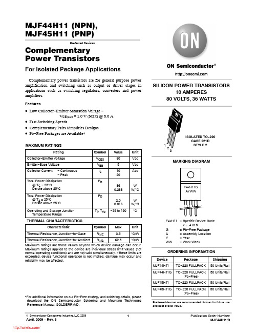
MJF44H11G;MJF45H11G;MJF44H11;MJF45H11;中文规格书,Datasheet资料
20 30 50 70 100
VCE, COLLECTOR-EMITTER VOLTAGE (VOLTS)
Figure 2. Maximum Rated Forward Bias Safe Operating Area
There are two limitations on the power handling ability of a transistor: average junction temperature and second breakdown. Safe operating area curves indicate IC − VCE limits of the transistor that must be observed for reliable operation; i.e., the transistor must not be subjected to greater dissipation than the curves indicate.
−
−
500
−
−
500
−
−
140
−
−
100
−
Unit Vdc mA mA Vdc Vdc
−
pF MHz
ns ns ns
r(t), TRANSIENT THERMAL RESISTANCE (NORMALIZED)
1.0 0.7 D = 0.5 0.5
0.3 0.2
0.2
0.1 0.1
0.07
0.05
0.05 0.02
MJF44H11 MJF45H11
Symbol VCEO(sus)
ICES IEBO VCE(sat) VBE(sat) hFE
W25Q128BVEIG;中文规格书,Datasheet资料

Publication Release Date: April 18, 20123V 128M-BITSERIAL FLASH MEMORY WITH DUAL AND QUAD SPITable of Contents1.GENERAL DESCRIPTION (5)2.FEATURES (5)3.PACKAGE TYPES AND PIN CONFIGURATIONS (6)3.1Pad Configuration WSON 8x6-mm (6)3.2Pad Description WSON 8x6-mm (6)3.3Pin Configuration SOIC 300-mil (7)3.4Pin Description SOIC 300-mil (7)3.5Ball Configuration TFBGA 8x6-mm (5x5 or 6x4 Ball Array) (8)3.6Ball Description TFBGA 8x6-mm (8)4.PIN DESCRIPTIONS (9)4.1Chip Select (/CS) (9)4.2Serial Data Input, Output and IOs (DI, DO and IO0, IO1, IO2, IO3) (9)4.3Write Protect (/WP) (9)4.4HOLD (/HOLD) (9)4.5Serial Clock (CLK) (9)5.BLOCK DIAGRAM (10)6.FUNCTIONAL DESCRIPTIONS (11)6.1SPI OPERATIONS (11)6.1.1Standard SPI Instructions (11)6.1.2Dual SPI Instructions (11)6.1.3Quad SPI Instructions (11)6.1.4Hold Function (11)6.2WRITE PROTECTION (12)6.2.1Write Protect Features (12)7.STATUS REGISTERS AND INSTRUCTIONS (13)7.1STATUS REGISTERS (13)7.1.1BUSY Status (BUSY) (13)7.1.2Write Enable Latch Status (WEL) (13)7.1.3Block Protect Bits (BP2, BP1, BP0) (13)7.1.4Top/Bottom Block Protect Bit (TB) (13)7.1.5Sector/Block Protect Bit (SEC) (13)7.1.6Complement Protect Bit (CMP) (14)7.1.7Status Register Protect Bits (SRP1, SRP0) (14)7.1.8Erase/Program Suspend Status (SUS) (14)7.1.9Security Register Lock Bits (LB3, LB2, LB1) (14)7.1.10Quad Enable Bit (QE) (15)7.1.11Status Register Memory Protection (CMP = 0) (16)7.1.12 Status Register Memory Protection (CMP = 1) (17)Publication Release Date: April 18, 20127.2 INSTRUCTIONS (18)7.2.1 Manufacturer and Device Identification ................................................................................ 18 7.2.2 Instruction Set Table 1 (Erase, Program Instructions) .......................................................... 19 7.2.3 Instruction Set Table 2 (Read Instructions) .......................................................................... 20 7.2.4 Instruction Set Table 3 (ID, Security Instructions) ................................................................ 21 7.2.5 Write Enable (06h) ............................................................................................................... 22 7.2.6 Write Enable for Volatile Status Register (50h) .................................................................... 22 7.2.7 Write Disable (04h) ............................................................................................................... 23 7.2.8 Read Status Register-1 (05h) and Read Status Register-2 (35h) ........................................ 24 7.2.9 Write Status Register (01h) .................................................................................................. 24 7.2.10 Read Data (03h) ................................................................................................................. 26 7.2.11 Fast Read (0Bh) ................................................................................................................. 27 7.2.12 Fast Read Dual Output (3Bh) ............................................................................................. 28 7.2.13 Fast Read Quad Output (6Bh) ............................................................................................ 29 7.2.14 Fast Read Dual I/O (BBh) ................................................................................................... 30 7.2.15 Fast Read Quad I/O (EBh) ................................................................................................. 32 7.2.16 Word Read Quad I/O (E7h) ................................................................................................ 34 7.2.17 Octal Word Read Quad I/O (E3h) ....................................................................................... 36 7.2.18 Set Burst with Wrap (77h) .................................................................................................. 38 7.2.19 Continuous Read Mode Bits (M7-0) ................................................................................... 39 7.2.20 Continuous Read Mode Reset (FFh or FFFFh) .................................................................. 39 7.2.21 Page Program (02h) ........................................................................................................... 40 7.2.22 Quad Input Page Program (32h) ........................................................................................ 41 7.2.23 Sector Erase (20h) ............................................................................................................. 42 7.2.24 32KB Block Erase (52h) ..................................................................................................... 43 7.2.25 64KB Block Erase (D8h) ..................................................................................................... 44 7.2.26 Chip Erase (C7h / 60h) ....................................................................................................... 45 7.2.27 Erase / Program Suspend (75h) ......................................................................................... 46 7.2.28 Erase / Program Resume (7Ah) ......................................................................................... 47 7.2.29 Power-down (B9h) .............................................................................................................. 48 7.2.30 Release Power-down / Device ID (ABh) ............................................................................. 49 7.2.31 Read Manufacturer / Device ID (90h) ................................................................................. 51 7.2.32 Read Manufacturer / Device ID Dual I/O (92h) ................................................................... 52 7.2.33 Read Manufacturer / Device ID Quad I/O (94h) ................................................................. 53 7.2.34 Read Unique ID Number (4Bh)........................................................................................... 54 7.2.35 Read JEDEC ID (9Fh) ........................................................................................................ 55 7.2.36 Read SFDP Register (5Ah) ................................................................................................ 56 7.2.37 Erase Security Registers (44h) ........................................................................................... 57 7.2.38 Program Security Registers (42h) ...................................................................................... 58 7.2.39 Read Security Registers (48h) . (59)8.ELECTRICAL CHARACTERISTICS (60)8.1Absolute Maximum Ratings (60)8.2Operating Ranges (60)8.3Power-up Timing and Write Inhibit Threshold (61)8.4DC Electrical Characteristics (62)8.5AC Measurement Conditions (63)8.6AC Electrical Characteristics (64)8.7AC Electrical Characteristics (cont’d) (65)8.8Serial Output Timing (66)8.9Serial Input Timing (66)8.10HOLD Timing (66)8.11WP Timing (66)9.PACKAGE SPECIFICATION (67)9.18-Pad WSON 8x6-mm (Package Code E) (67)9.216-Pin SOIC 300-mil (Package Code F) (68)9.324-Ball TFBGA 8x6-mm (Package Code B, 5x5-1 Ball Array) (69)9.424-Ball TFBGA 8x6-mm (Package Code C, 6x4 Ball Array) (70)10.ORDERING INFORMATION (71)10.1Valid Part Numbers and Top Side Marking (72)11.REVISION HISTORY (73)Publication Release Date: April 18, 20121. GENERAL DESCRIPTIONThe W25Q128BV (128M-bit) Serial Flash memory provides a storage solution for systems with limited space, pins and power. The 25Q series offers flexibility and performance well beyond ordinary Serial Flash devices. They are ideal for code shadowing to RAM, executing code directly from Dual/Quad SPI (XIP) and storing voice, text and data. The device operates on a single 2.7V to 3.6V power supply with current consumption as low as 4mA active and 1µA for power-down.The W25Q128BV array is organized into 65,536 programmable pages of 256-bytes each. Up to 256 bytes can be programmed at a time. Pages can be erased in groups of 16 (4KB sector erase), groups of 128 (32KB block erase), groups of 256 (64KB block erase) or the entire chip (chip erase). The W25Q128BV has 4,096 erasable sectors and 256 erasable blocks respectively. The small 4KB sectors allow for greater flexibility in applications that require data and parameter storage. (See Figure 2.)The W25Q128BV supports the standard Serial Peripheral Interface (SPI), and a high performance Dual/Quad output as well as Dual/Quad I/O SPI: Serial Clock, Chip Select, Serial Data I/O0 (DI), I/O1 (DO), I/O2 (/WP), and I/O3 (/HOLD). SPI clock frequencies of up to 104MHz are supported allowing equivalent clock rates of 208MHz (104MHz x 2) for Dual Output and 280MHz (70MHz x 4) for Quad SPI when using the Fast Read Quad SPI instructions. These transfer rates can outperform standard Asynchronous 8 and 16-bit Parallel Flash memories. The Continuous Read Mode allows for efficient memory access with as few as 8-clocks of instruction-overhead to read a 24-bit address, allowing true XIP (execute in place) operation.A Hold pin, Write Protect pin and programmable write protection, with top, bottom or complement array control, provide further control flexibility. Additionally, the device supports JEDEC standard manufacturer and device identification with a 64-bit Unique Serial Number.2. FEATURES• Family of SpiFlash Memories – W25Q128BV: 128M-bit/16M-byte – 256-byte per programmable page– Standard SPI: CLK, /CS, DI, DO, /WP, /Hold– Dual SPI: CLK, /CS, IO 0, IO 1, /WP, /Hold– Quad SPI: CLK, /CS, IO 0, IO 1, IO 2, IO 3• Highest Performance Serial Flash– 104/70MHz Dual Output/Quad SPI clocks– 208/280MHz equivalent Dual /Quad SPI– 35MB/S continuous data transfer rate– Up to 5X that of ordinary Serial Flash– More than 100,000 erase/program cycles (1)– More than 20-year data retention• Efficient “Continuous Read Mode” – Low Instruction overhead– Continuous Read with 8/16/32/64-Byte Wrap – As few as 8 clocks to address memory – Allows true XIP (execute in place) operation – Outperforms X16 Parallel Flash • Low Power, Wide Temperature Range– Single 2.7 to 3.6V supply– 4mA active current, <1µA Power-down current – -40°C to +85/105°C operating range • Flexible Architecture with 4KB sectors– Uniform Sector/Block Erase (4K/32K/64K-Byte)– Program one to 256 bytes– Erase/Program Suspend & Resume• Advanced Security Features – Software and Hardware Write-Protect – Top/Bottom, 4KB complement array protection – Lock-Down and OTP array protection – 64-Bit Unique Serial Number for each device – Discoverable Parameters (SFDP) Register – 3X256-Byte Security Registers with OTP locks– Volatile & Non-volatile Status Register Bits• Space Efficient Packaging – 8-pad WSON 8x6-mm – 16-pin SOIC 300-mil – 24-ball TFBGA 8x6-mm– Contact Winbond for KGD and other options Note 1. More than 100k Block Erase/Program cycles for Industrial and Automotive temperature; more than 10k fullchip Erase/Program cycles tested in compliance with AEC-Q100.3.PACKAGE TYPES AND PIN CONFIGURATIONSW25Q128BV is offered in an 8-pad WSON 8x6-mm (package code E), a 16-pin SOIC 300-mil (package code F) and two 24-ball 8x6-mm TFBGAs (package code B, C) as shown in Figure 1a-c respectively. Package diagrams and dimensions are illustrated at the end of this datasheet.3.1Pad Configuration WSON 8x6-mmFigure 1a. W25Q128BV Pad Assignments, 8-pad WSON 8x6-mm (Package Code E)3.2Pad Description WSON 8x6-mmPAD NO. PAD NAME I/O FUNCTION1 /CS I Chip Select Input2 DO (IO1) I/O Data Output (Data Input Output 1)*1(IO2)I/O Write Protect Input ( Data Input Output 2)*23 /WP4 GND Ground5 DI (IO0) I/O Data Input (Data Input Output 0)*16 CLK I Serial Clock Input(IO3)I/O Hold Input (Data Input Output 3)*27 /HOLD8 VCC PowerSupply*1: IO0 and IO1 are used for Standard and Dual SPI instructions*2: IO0 – IO3 are used for Quad SPI instructionsPublication Release Date: April 18, 20123.3 Pin Configuration SOIC 300-milFigure 1b. W25Q128BV Pin Assignments, 16-pin SOIC 300-mil (Package Code F)3.4 Pin Description SOIC 300-milPIN NO.PIN NAMEI/OFUNCTION1 /HOLD (IO3)I/OHold Input (Data Input Output 3)*22 VCC Power Supply3 N/C No Connect4 N/C No Connect5 N/C No Connect6 N/C No Connect7 /CS I Chip Select Input8DO (IO1)I/O Data Output (Data Input Output 1)*19 /WP (IO2)I/OWrite Protect Input (Data Input Output 2)*210 GND Ground 11 N/C No Connect 12 N/C No Connect 13 N/C No Connect 14 N/C No Connect 15 DI (IO0) I/O Data Input (Data Input Output 0)*116CLKISerial Clock Input*1: IO0 and IO1 are used for Standard and Dual SPI instructions.*2: IO0 – IO3 are used for Quad SPI instructions, /WP or /HOLD functions are only available for Standard/Dual SPI.3.5Ball Configuration TFBGA 8x6-mm (5x5 or 6x4 Ball Array)Figure 1c. W25Q128BV Ball Assignments, 24-ball TFBGA 8x6-mm (Package Code B, C)3.6Ball Description TFBGA 8x6-mmBALL NO. PIN NAME I/O FUNCTIONB2 CLK I Serial Clock InputB3 GND GroundSupplyB4 VCC PowerC2 /CS I Chip Select Input(IO2)I/O Write Protect Input (Data Input Output 2)*2C4 /WPD2 DO (IO1) I/O Data Output (Data Input Output 1)*1D3 DI (IO0) I/O Data Input (Data Input Output 0)*1(IO3)I/O Hold Input (Data Input Output 3)*2D4 /HOLDMultiple NC NoConnect*1: IO0 and IO1 are used for Standard and Dual SPI instructions.*2: IO0 – IO3 are used for Quad SPI instructions, /WP or /HOLD functions are only available for Standard/Dual SPI.Publication Release Date: April 18, 20124. PIN DESCRIPTIONS4.1 Chip Select (/CS)The SPI Chip Select (/CS) pin enables and disables device operation. When /CS is high the device is deselected and the Serial Data Output (DO, or IO0, IO1, IO2, IO3) pins are at high impedance. When deselected, the devices power consumption will be at standby levels unless an internal erase, program or write status register cycle is in progress. When /CS is brought low the device will be selected, power consumption will increase to active levels and instructions can be written to and data read from the device. After power-up, /CS must transition from high to low before a new instruction will be accepted. The /CS input must track the VCC supply level at power-up (see “Write Protection” and Figure 38). If needed a pull-up resister on /CS can be used to accomplish this.4.2 Serial Data Input, Output and IOs (DI, DO and IO0, IO1, IO2, IO3)The W25Q128BV supports standard SPI, Dual SPI and Quad SPI operation. Standard SPI instructions use the unidirectional DI (input) pin to serially write instructions, addresses or data to the device on the rising edge of the Serial Clock (CLK) input pin. Standard SPI also uses the unidirectional DO (output) to read data or status from the device on the falling edge of CLK.Dual and Quad SPI instructions use the bidirectional IO pins to serially write instructions, addresses or data to the device on the rising edge of CLK and read data or status from the device on the falling edge of CLK. Quad SPI instructions require the non-volatile Quad Enable bit (QE) in Status Register-2 to be set. When QE=1, the /WP pin becomes IO2 and /HOLD pin becomes IO3.4.3 Write Protect (/WP)The Write Protect (/WP) pin can be used to prevent the Status Register from being written. Used in conjunction with the Status Register’s Block Protect (CMP, SEC, TB, BP2, BP1 and BP0) bits and Status Register Protect (SRP) bits, a portion as small as a 4KB sector or the entire memory array can be hardware protected. The /WP pin is active low. When the QE bit of Status Register-2 is set for Quad I/O, the /WP pin function is not available since this pin is used for IO2. See Figure 1a-c for the pin configuration of Quad I/O operation.4.4 HOLD (/HOLD)The /HOLD pin allows the device to be paused while it is actively selected. When /HOLD is brought low, while /CS is low, the DO pin will be at high impedance and signals on the DI and CLK pins will be ignored (don’t care). When /HOLD is brought high, device operation can resume. The /HOLD function can be useful when multiple devices are sharing the same SPI signals. The /HOLD pin is active low. When the QE bit of Status Register-2 is set for Quad I/O, the /HOLD pin function is not available since this pin is used for IO3. See Figure 1a-c for the pin configuration of Quad I/O operation.4.5 Serial Clock (CLK)The SPI Serial Clock Input (CLK) pin provides the timing for serial input and output operations. ("See SPI Operations")5.BLOCK DIAGRAM ArrayFigure 2. W25Q128BV Serial Flash Memory Block Diagram分销商库存信息: WINBONDW25Q128BVEIG。
BUL44;BUL44G;中文规格书,Datasheet资料

VCE, VOLTAGE (VOLTS)
1.0
0.01
0.1
1.0
10
IC, COLLECTOR CURRENT (AMPS)
Characteristic
Symbol
Min
OFF CHARACTERISTICS
Collector−Emitter Sustaining Voltage (IC = 100 mA, L = 25 mH)
Collector Cutoff Current (VCE = Rated VCEO, IB = 0)
400
ICEO
−
ICES
−
−
−
IEBO
−
ON CHARACTERISTICS
Base−Emitter Saturation Voltage (IC = 0.4 Adc, IB = 40 mAdc) (IC = 1.0 Adc, IB = 0.2 Adc)
Collector−Emitter Saturation Voltage (IC = 0.4 Adc, IB = 40 mAdc)
BUL44G
SWITCHMODEt NPN Bipolar Power Transistor
For Switching Power Supply Applications
The BUL44G have an applications specific state−of−the−art die designed for use in 220 V line operated Switchmode Power supplies and electronic light ballasts.
Features
D45H11;中文规格书,Datasheet资料

D45H11 — PNP Power Amplifier© 2012 Fairchild Semiconductor Corporation D45H11 Rev. A11June 2012D45H11PNP Power Amplifier•This device is designed for power amplifier, regulator and switching circuits where speed is important.•Sourced from process 5Q.Absolute Maximum RatingsElectrical Characteristics T a = 25°C unless otherwise notedThermal Characteristics T a = 25°C unless otherwise noted* Note) Device mounted on FR-$ PCB 36mm*18mm*1.5mm: Mounting pad for the collector lead min. 6cm2.SymbolParameterValueUnitsV CEO Collector-Emitter Voltage-80V I C Collector Current - Continuous-10A T J , T STGOperating and Storage Junction Temperature Range-55 to +150°CSymbolParameter Test Condition Min.Max.UnitsOff Characteristics V (BR)CEO Collector-Emitter Breakdown Voltage I C = -100mA, I B = 0-80V I CBO Collector-Cutoff Current V CB = -80V, I E = 0-10μA I EBO Emitter-Cutoff Current V EB = -5V, I C = 0-100μAOn Characteristics *h FE DC Current GainV CE = -1V, I C = -2A V CE = -1V, I C = -4A 6040V CE (sat)Collector-Emitter Saturation Voltage I C = -8A,I B = -0.4A -1.0V V BE (sat)Base-Emitter Saturation Voltage I C = -8A,I B = -0.8A -1.5V V BE (on)Base-Emitter On Voltage V CE = -2V, I C = -10mA -0.54-0.65V Small Signal Characteristicsf TCurrent Gain Bandwidth ProductI C = -500mA, V CE = -10V40MHZSymbolParameterMax.UnitsP D Total Device DissipationDerate above 25°C60480W mW/°C R θJC Thermal Resistance, Junction to Case 2.1°C/W R θJAThermal Resistance, Junction to Ambient62.5°C/W1TO-2201. Base2. Collector3. EmitterMark: D45H11The following includes registered and unregistered trademarks and service marks, owned by Fairchild Semiconductor and/or its global subsidiaries, and is notAX-CAP¥*BitSiC¥Build it Now¥CorePLUS¥CorePOWER¥CROSSVOLT¥CTL¥Current Transfer Logic¥DEUXPEED®Dual Cool™ EcoSPARK®EfficientMax¥ESBC¥®Fairchild®Fairchild Semiconductor®FACT Quiet Series¥FACT®FAST®FastvCore¥FETBench¥FlashWriter®*FPS¥Global Power ResourceGreenBridge¥Green FPS¥Green FPS¥ e-Series¥G max¥GTO¥IntelliMAX¥ISOPLANAR¥Making Small Speakers Sound Louderand Better™MegaBuck¥MICROCOUPLER¥MicroFET¥MicroPak¥MicroPak2¥MillerDrive¥MotionMax¥Motion-SPM¥mWSaver¥OptoHiT¥OPTOLOGIC®OPTOPLANAR®®Programmable Active Droop¥QFET®QS¥Quiet Series¥RapidConfigure¥¥Saving our world, 1mW/W/kW at a time™SignalWise¥SmartMax¥SMART START¥Solutions for Your Success¥SPM®STEALTH¥SuperFET®SuperSOT¥-3SuperSOT¥-6SuperSOT¥-8SupreMOS®SyncFET¥Sync-Lock™®*The Power Franchise®TinyBoost¥TinyBuck¥TinyCalc¥TinyLogic®TINYOPTO¥TinyPower¥TinyPWM¥TinyWire¥TranSiC¥TriFault Detect¥TRUECURRENT®*P SerDes¥UHC®Ultra FRFET¥UniFET¥VCX¥VisualMax¥VoltagePlus¥XS™* Trademarks of System General Corporation, used under license by Fairchild Semiconductor.DISCLAIMERFAIRCHILD SEMICONDUCTOR RESERVES THE RIGHT TO MAKE CHANGES WITHOUT FURTHER NOTICE TO ANY PRODUCTS HEREIN TO IMPROVE RELIABILITY, FUNCTION, OR DESIGN. FAIRCHILD DOES NOT ASSUME ANY LIABILITY ARISING OUT OF THE APPLICATION OR USE OF ANY PRODUCT OR CIRCUIT DESCRIBED HEREIN; NEITHER DOES IT CONVEY ANY LICENSE UNDER ITS PATENT RIGHTS, NOR THE RIGHTS OF OTHERS. THESE SPECIFICATIONS DO NOT EXPAND THE TERMS OF FAIRCHILD’S WORLDWIDE TERMS AND CONDITIONS, SPECIFICALLY THE WARRANTY THEREIN, WHICH COVERS THESE PRODUCTS.LIFE SUPPORT POLICYFAIRCHILD’S PRODUCTS ARE NOT AUTHORIZED FOR USE AS CRITICAL COMPONENTS IN LIFE SUPPORT DEVICES OR SYSTEMS WITHOUT THE EXPRESS WRITTEN APPROVAL OF FAIRCHILD SEMICONDUCTOR CORPORATION.As used herein:1. Life support devices or systems are devices or systems which, (a)are intended for surgical implant into the body or (b) support or sustain life, and (c) whose failure to perform when properly used in accordance with instructions for use provided in the labeling, can be reasonably expected to result in a significant injury of the user. 2. A critical component in any component of a life support, device, orsystem whose failure to perform can be reasonably expected to cause the failure of the life support device or system, or to affect its safety or effectiveness.ANTI-COUNTERFEITING POLICYFairchild Semiconductor Corporation's Anti-Counterfeiting Policy. Fairchild's Anti-Counterfeiting Policy is also stated on our external website, , under Sales Support.Counterfeiting of semiconductor parts is a growing problem in the industry. All manufacturers of semiconductor products are experiencing counterfeiting of their parts. Customers who inadvertently purchase counterfeit parts experience many problems such as loss of brand reputation, substandard performance, failed applications, and increased cost of production and manufacturing delays. Fairchild is taking strong measures to protect ourselves and our customers from the proliferation of counterfeit parts. Fairchild strongly encourages customers to purchase Fairchild parts either directly from Fairchild or from Authorized Fairchild Distributors who are listed by country on our web page cited above. Products customers buy either from Fairchild directly or from Authorized Fairchild Distributors are genuine parts, have full traceability, meet Fairchild's quality standards for handling and storage and provide access to Fairchild's full range of up-to-date technical and product information. Fairchild and our Authorized Distributors will stand behind all warranties and will appropriately address any warranty issues that may arise. Fairchild will not provide any warranty coverage or other assistance for parts bought from Unauthorized Sources. Fairchild is committed to combat this global problem and encourage our customers to do their part in stopping this practice by buying direct or from authorized distributors.PRODUCT STATUS DEFINITIONSDefinition of TermsDatasheet Identification Product Status DefinitionAdvance Information Formative / In DesignDatasheet contains the design specifications for product development. Specifications may change分销商库存信息: FAIRCHILDD45H11。
EMC45DRYI中文资料(List Unclassifed)中文数据手册「EasyDatasheet - 矽搜」

106.68 109.22 121.92 124.46 129.54 149.86
B
+_ 0.20
12.70 15.24 17.78 20.32 22.86
27.94 33.02 35.56 40.64 45.72 48.26
50.80 53.34 58.42 60.96 66.04 68.58
.275 [6.98]
.225 [5.72]
字母b SIDE
0.016 [0.41]厚, 总体PLATED ONLY
.007 [0.18] THICK
EYELET (TE)
EYELET (RE)
FITS .043 [1.09]
直角
(RA)
.125 [3.18]
.185 [4.70]
.050 [1.27]
C = PPS /铍镍(咨询工厂) N = PEEK /铍铜(咨询工厂) W = PEEK /铍镍(咨询工厂)
F = PPS / Pfinodal ***(咨询工厂)
咨询工厂其他材料
触点表面涂层
接触面
Z = 0.000010"金 X = 0.000030"金 G = 0.000010"金奖 Y = 0.000030"金奖
5.275 5.575
5.475 5.775
6.275 6.575
ቤተ መጻሕፍቲ ባይዱ
E
+_.020
1.275 1.375 1.475 1.575 1.675
1.875 2.075 2.175 2.375 2.575 2.675
2.775 2.875 3.075 3.175 3.375 3.475
新世纪LED芯片45mil规格书

V.990105BCONTROLLEDDOCUMENTAPPROVAL SHEETProduct Type:Blue InGaN/ GaN LED DP5 (45X45) ChipsPart No: B4545ECD0Doc ID: MK-QA-010 Rev: E.Date : January 05, 2010Created By: Approved By:Heaven HsuO scar Chan Heaven HsuV.990105B 1.Scope:This specification applies to Blue InGaN/GaN LED chips,DP5(45X45) of Genesis Photonics Inc.。
And Includes the inspection of electro-optical characteristics。
2.Materials:2.1 P-contact:ITO。
2.2 P-pad:Au。
2.3 N-pad:Au。
3.Mechanical specifications :3.1 Chip size:1143×1143µm ( ± 10µm )。
3.2 P-pad:φ 110µm ( ± 10µm )。
3.3 N-pad:φ 110µm ( ± 10µm )。
3.4 Chip thickness:150µm ( ± 10µm )。
3.5 Chip diagramTop view Cross section4.Electro-optical characteristics and specification:4.1 Test condition:Parameter Symbol Condition UnitDominant wavelength Wd If = 350 mA nmLuminous intensity Iv If = 350 mA mWForward voltage Vf If = 350 mA VReverse current Ir Vr = - 5 V µAV.990105B4.2 Characteristics:Maximum Ratings at T a=25℃Symbol Conditions RatingsDC Forward Current I F T j=125℃700mAJunction Temperature T j150℃Reverse Voltage V r T a=25℃-5VReverse Current I r V r=-5V<2µAAssembly Process Temp. 325℃(<5sec)Notes:Maximum ratings were measured in an integrating sphere using Au plated TO-39 headers without an encapsulate, and may differ with different package types..4.3 Model No:Part No : A B C D E F G H IBin : 1 2 3 4 5 6 7 – 8 9Exp:Part No: B4545ECD0Bin : V33 P45A-294.3.1 Code A B C D E F G H I :Product code: A B C D E F G H IProduct code4.3.2 Code 1 2 3 :Vf range(V): 1 2 3V31 3.1~3.2 V32 3.2~3.3 V33 3.3~3.4 V34 3.4~3.54.3.3 Code 4 :Electrical spec: 4P Vf<3.5 ; Ir<2µAV.990105B4.3.4 Code 5 6 7 :Wd range(nm): 5 6 744B 442.5~445.0 45A 450.0~452.5 45D 457.5~460.044C 445.0~447.5 45B 452.5~455.0 46A 460.0~462.544D 447.5~450.0 45C 455.0~457.5 46B 462.5~465.04.3.5 Code 8 9 :Iv range (mW): 8 926 180~20027 200~22028 220~24029 240~26030 260~28031 280~300Lot No:L/N: A B C D E – F G H I J – K L MExp:L/N:61621-18183-0015.Bin description:Below is a table which defines the specific part numbers or “bins” which are within the B4545ECD0 kit. Each tape will contain chips from only one bin, and a customer order for kit B4545ECD0 will befulfilled with a shipment of production devices which may contain any combination of tapesconsisting of any or all bins in the table.Wd Grade Iv Grade45A -29 -30 -3145B -29 -30 -3145C -29 -30 -3145D -28 -29 -30 -3146A -28 -29 -30 -3146B -28 -2946C -27 -28 -2946D -27 -28V.990105B6. Packing specification :6.1 LED chips are placed on the blue adhesive tape with the bonding pads facing up (i.e. sapphireis adhered to the tape) and covered with a glossy paper (See Figure 6-1)6.2 Chip array must be placed within the center of the blue adhesive tape and the bar code label islocated on the back of the blue tape at the left lower corner (See Figure. 6-2).6.3 Label specification :MIN AVG MAX STD Vf (V) -- actual spec actual Iv (mW) spec actual spec actual Wd (nm) spec actual spec actual6.4 Packaging dimensions (See table 6-1)ItemDimensionBlue adhesive tape 200 mm × 200 mm (±10mm) Mesh curtain 70 mm × 70 mm (±10mm) Backing glossy paper 200 mm × 210 mm (±10mm) Label location on blue tapeLower left corner; 10 ± 2 mmFig 6-1 Chip on tapeFig 6-2 Location of labelTable 6-1 Package dimensionsV.990105B6.5 Packaging for shipment6.5.1 The sheet (blue adhesion tape +mesh curtain+ glossy paper) must be packed in ananti-electrostatic bag and paper box for shipment(See Fig 6-3)6.5.2 The max numbers of blue tapes in a bag is 20 pieces 6.5.3 The ESD attention label is stamped on bag6.5.4 Each box and each sheet should be labeled with information describing its content.BagShipping AddressPacking ListESD labelV.990105BCriteria of Defective Chip1. Inspection Equipment and Method Inspecting Chip by Microscope Magnification: 30X2. Figure of ExampleItemDefective itemCriteria of Defect ChipExample1 Active Area Broken Rejected2 Active Area Dirty (1)Dirty Area≥ 10% of Active Area3Active Layer Breakage and Scratched1. Breakage and scratch must not cross active layer2. Breakage and Scratch ≥ 10% of Active Layer4Pad DirtyDirty Area≥ 10% of Pad AreaV.990105BItem Defective item Criteria of Defect Chip Example5 Pad Scratched1.Scratched Area ≥ 20% of Pad Area2.Scratched Length ≥ 1/3 of Pad Diameter3.Exposed Sub-tract6 Remnant Metal1. Remnant Area≥ 10% of Active Area2. Remnant metal ≥ 3 Spots and Spot Length ≥ 20 μm3. Remnant metal over active area7 Defective Scribe1. Double Chips2. Scribed on active area or N-pad3. Racked or Chipped Area ≥ 10% of the Original Area4. Un-scribed Area≥ 110% of the Original Area9Wrong LabelRejected --10 Inverse Protective Paper Rejected-- 11 The Amount of ChipsAmount per Blue Tape ≥ 50 pcs--V.990105BDominant wavelength shift vs Forward currentRelative luminous intensity vs Forward currentV.990105B Led Chip View angle Measurement1.Package typeChip on TO-39 Without Cap2.Measurement ConditionMeasurement Distance: 100mmOperating Angle From -900 to 9003.ResultRelative Intensity vs. Off Axis Angle ( View Angle)50% Power Angle:122.5 degreeNotes:The above diagram is measured with the current at 200mA using Au plated To39 headers without an encapsulate.。
- 1、下载文档前请自行甄别文档内容的完整性,平台不提供额外的编辑、内容补充、找答案等附加服务。
- 2、"仅部分预览"的文档,不可在线预览部分如存在完整性等问题,可反馈申请退款(可完整预览的文档不适用该条件!)。
- 3、如文档侵犯您的权益,请联系客服反馈,我们会尽快为您处理(人工客服工作时间:9:00-18:30)。
VCE(sat) VCE(sat) hFE
Vdc Vdc --
Dynamic Saturation Voltage: Determined 1.0 ms and 3.0 ms respectively after rising IB1 reaches 90% of final IB1 (see Figure 18)
Characteristic OFF CHARACTERISTICS Collector--Emitter Sustaining Voltage (IC = 100 mA, L = 25 mH) Collector Cutoff Current (VCE = Rated VCEO, IB = 0) Collector Cutoff Current (VCE = Rated VCES, VEB = 0) (TC = 125C) Emitter Cutoff Current (VEB = 9.0 Vdc, IC = 0) ON CHARACTERISTICS Base--Emitter Saturation Voltage (IC = 1.0 Adc, IB = 0.2 Adc) (IC = 2.0 Adc, IB = 0.4 Adc) Collector--Emitter Saturation Voltage (IC = 1.0 Adc, IB = 0.2 Adc) (TC = 125C) Collector--Emitter Saturation Voltage (IC = 2.0 Adc, IB = 0.4 Adc) (TC = 125C) DC Current Gain (IC = 0.3 Adc, VCE = 5.0 Vdc) (IC = 2.0 Adc, VCE = 1.0 Vdc) (IC = 10 mAdc, VCE = 5.0 Vdc) DYNAMIC CHARACTERISTICS Current Gain Bandwidth (IC = 0.5 Adc, VCE = 10 Vdc, f = 1.0 MHz) Output Capacitance (VCB = 10 Vdc, IE = 0, f = 1.0 MHz) Input Capacitance (VEB = 8.0 Vdc) (IC = 1.0 Adc IB1 = 100 mAdc VCC = 300 V) (IC = 2.0 Adc IB1 = 400 mAdc VCC = 300 V) 1.0 ms 3.0 ms 1.0 ms 3.0 ms (TC = 125C) (TC = 125C) (TC = 125C) (TC = 125C) ton toff VCE (Dyn sat) fT Cob Cib ---------------70 -2.6 ------------12 50 920 1.75 4.4 0.5 1.0 1.85 6.0 0.5 1.0 75 120 2.8 3.5 -200 -4.2 230 400 110 100 1.1 1.5 170 170 80 0.6 175 — 75 1200 --------110 -3.5 -170 -3.8 -350 -150 -1.7 -250 -120 0.9 300 ns ms MHz pF pF (TC = 125C) (TC = 125C) VBE(sat) ------14 -7.0 5.0 10 0.84 0.89 0.175 0.150 0.25 0.275 -32 14 12 22 1.2 1.25 0.25 -0.4 -34 ----Vdc VCEO(sus) ICEO ICES IEBO 400 ----------100 10 100 100 Vdc mAdc mAdc mAdc Symbol Min Typ Max Unit
TJ = 25C VCE , VOLTAGE (VOLTS)
VCE , VOLTAGE (VOLTS)
1.5 1 A 1.5 2 A A 3A 4A 5A 6A
1.0
1.0
0.1
IC/IB = 10 IC/IB = 5 TJ = 25C TJ = 125C 0.10 1.00 10.00
0.5 IC = 0.5 A 0 0.01
Stresses exceeding Maximum Ratings may damage the device. Maximum Ratings are stress ratings only. Functional operation above the Recommended Operating Conditions is not implied. Extended exposure to stresses above the Recommended Operating Conditions may affect device reliability. 1. Pulse Test: Pulse Width = 5 ms, Duty Cycle 10%.
1 0.01
0.10
1.00
10.00
1 0.01
0.10
1.00
10.00
IC, COLLECTOR CURRENT (AMPS)
IC, COLLECTOR CURRENT (AMPS)
Figure 1. DC Current Gain @ 1 Volt
2.0 10
Figure 2. DC Current Gain at @ 5 Volts
Features
Improved Efficiency Due to:
Low Base Drive Requirements (High and Flat DC Current Gain hFE) Low Power Losses (On-State and Switching Operations) Fast Switching: tfi = 100 ns (typ) and tsi = 3.2 ms (typ) @ IC = 2.0 A, IB1 = IB2 = 0.4 A Full Characterization at 125C Tight Parametric Distributions Consistent Lot--to--Lot These Devices are Pb--Free and are RoHS Compliant*
BUL45G NPN Silicon Power Transistor
High Voltage SWITCHMODE Series
Designed for use in electronic ballast (light ballast) and in SWITCHMODE Power supplies up to 50 W.
MAXIMUM RATINGS
Rating Collector--Emitter Sustaining Voltage Collector--Base Breakdown Voltage Emitter--Base Voltage Collector Current Base Current Total Device Dissipation @ TC = 25_C Derate above 25C Operating and Storage Temperature -- Continuous -- Peak (Note 1) Symbol VCEO VCES VEBO IC ICM IB PD TJ, Tstg Value 400 700 9.0 5.0 10 2.0 75 0.6 --65 to 150 Unit Vdc Vdc Vdc Adc Adc W W/_C _C
ORDERING INFORMATION
Device BUL45G Package TO--220 (Pb--Free) Shipping 50 Units / Rail
*For additional information on our Pb--Free strategy and soldering details, please download the ON Semiconductor Soldering and Mounting Techniques Reference Manual, SOLDERRM/D.
Vdc
SWITCHING CHARACTERISTICS: Resistive Load Turn--On Time Turn--Off Time (IC = 2.0 Adc, IB1 = IB2 = 0.4 Adc Pulse Width = 20 ms, (TC = 125C) Duty Cycle < 20% VCC = 300 V (TC = 125C) (IC = 2.0 Adc, IB1 = 0.4 Adc IB2 = 0.4 Adc)
SWITCHING CHARACTERISTICS: Inductive Load (VCC = 15 Vdc, LC = 200 mH, Vclamp = 300 Vdc) Fall Time Storage Time Crossover Time Fall Time Storage Time Crossover Time Fall Time Storage Time Crossover Time (TC = 125C) (TC = 125C) (TC = 125C) (IC = 1.0 Adc, IB1 = 100 mAdc (TC = 125C) IB2 = 0.5 Adc) (TC = 125C) (TC = 125C) (IC = 2.0 Adc, IB1 = 250 mAdc (TC = 125C) IB2 = 2.0 Adc) (TC = 125C) (TC = 125C) tfi tsi tc tfi tsi tc tfi tsi tc ns ms ns ns ms ns ns ms ns
2
/
BUL45G