The Ratio of the Direct Photon Production Cross Section at 630 GeV and at 1800 GeV
Fluorescence Spectroscopy - 朝阳科技大学荧光光谱朝阳科技大学-40页文档资料
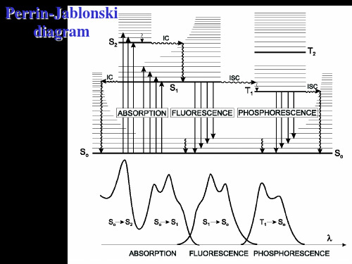
S is singlet and T is triplet.
The S0 state is the ground state and the subscript numbers identify individual states.
Energy level of MO
• Since emitted light only from the middle of the cuvette is detected the concentration must be low to assure accurate FF measurements.
Inner Filter Effect
Measurement of fluorescence quantum yields
em
em
fraction of intensity emitted at that fraction of total fluorescence
particular wavelength
that is detected
I0(ex)
If
(em)
=
IAbs
. (ex)
f
.
f(em).
K
em
em
fluorescence quantum yield
absorbed intensity at ex
I a ( b e ) s x I 0 (e ) 1 x 1 A (e 0 )x
measured intensity of fluorescence at em
Quantum Yield
Quantum Yield = FF • FF = number of fluorescence quanta emitted divided by number of quanta absorbed to a singlet excited state
放射物理单词
vacancy:空的
favored:可能是拼错了
Auger:同锇歇电子
Fraction:部分
Isomer:同质异能素(质子数和中子数都同,核能态不同)
Enunciate:清晰讲述/解释等
Penetrate:穿过
Instructive:指导的
nitrogen 氮
Chapter 4 (2)
1. dosimetry 放射剂量学
2. tissue-air 组织
3. backscatter逆散射
4. depict 描述 描写
5. irradiate 辐射 照射
6. calibration 教标
7. dosimeter 放射剂量计
perturb 扰动 摄动
homogeneous 同类的, 相似的
photon 光子
negligible 可忽略的
perturbation 扰动 摄动
finite 有限的
geometry 几何
composite 组成
equivalent 等效
affix 词缀 使附于
bracket 括号
Cumulate:应该是 accumulate 积累
Hypothetical:假设
Exponentially:指数地
rectangle :长方形
dosage:剂量值
proportional: 正比的
vertical:垂直的
horizontal:水平的
intersection:交叉的
collision 碰撞
bremsstrahlung 轫致(辐射)
一维光子晶体的能带结构计算与分析

medium layer A which is one of medium layers composing the photonic crystal at first,
or the optical thickness of the substitute layer is even times of A.By contraries,when
effects and new techniques.Hence it is essential to study the relationship between
structures and photonic band gaps. Transfer matrix method is a powerful and straightforward tool to analysis the band
dependence with the ratio of the medium layer’S refractive index which components the 1 D photonlc crystal,the larger the ratio of the refractive index(na/rib),the wider the
even times of COo.The relation ship between photonic band gap of 1 D temary photonic
medium crystal and the refractive index,thickness,number of the
layer is similar to 1 D
dielectric constant which can create some ranges of forbidden frequencies for
激光器驱动电路中英文翻译
中文2540字Laser driver circuitSmall changes will directly semiconductor laser drive current to the output intensity fluctuation. To stabilize the output power semiconductor laser, V oltage negative feedback principle to design a constant current driving circuit comprises a soft starting and current limiting protection circuit based on; At the same time, according to the need of the light source is modulated to eliminate the influence of background light and, integrated laser modulation circuit comprises a crystal oscillation circuit and divider circuit design. Making the specific circuit and complete the relevant experimental. The experimental results show that the circuit can provide a driving current of high stability, Current stability up to 0.05%; Soft start and current-limiting protection circuit can protect the semiconductor laser and enhance the impact capability. Modulation circuit generates a carrier signal needed for laser diode modulation and direct to complete the output light modulation, The switch can be conveniently realized from 256Hz to 512kHz range of 12 kinds of commonly used modulation frequency selection.Semiconductor laser with its excellent characteristics, high efficiency, simple structure, small is widely used in scientific research, national defense, medical, and other areas of processing, its drive technology becomes more and more important. Semiconductor laser is the ideal electron - photon direct conversion devices, quantum efficiency is very high, the current small changes will lead to a great change, the output light intensity of the therefore, semiconductor laser drive current requirements is very high. Driving technology of semiconductor laser usually adopts constant current drive mode, this work, through the principle of negative feedback control loop, directly provide the effective control of the drive current. In addition, the transient current or voltage spikes, and overcurrent, overvoltage will damage the semiconductor laser drive circuit, therefore should be considered in the protection circuit against electric shock measures and special.In some applications, DC semiconductor lasers produce DC drive light in the measurement process is vulnerable to interference from ambient light slow change, which could not be separated from the environment light required DC optical signal, the signal-to-noise ratio is too small, so to carry on the modulation. When the high-speed modulated semiconductor lasers, there will be dynamic characteristics iscomplex, such as the relaxation oscillation, since the pulse and multi-pulse phenomena. In this paper, experiments were conducted to study the characteristics of low frequency modulation. Semiconductor laser output is stable, and can be directly modulated, it has been widely applied in optical system, is the preferred source sensor system. This paper describes the design of a high stability driving current, modulation, simple operation and low cost driving circuit for the light source of optical fiber systems.In this paper, the design of driving the semiconductor laser modulation circuit composed of four parts, including constant current circuit, a soft start, current limit protection and modulation signal generating circuit. The constant current circuit to generate a high stable drive current. Soft start is the role of eliminating surge may be present in the circuit, to prevent the harm of surge for laser. To avoid damage due to overcurrent caused by semiconductor laser can not be restored, then adding current-limiting protection in a driver circuit. Circuit to realize the modulation and frequency can be adjusted to generate a modulated signal.The constant current circuit is shown in figure 1, The in-phase end voltage reference Vr into A1 op amp, the operational control amplifier conducting level, and thus to obtain the corresponding output current. The output current generated by sampling voltage sampling resistor Rs, the sampling voltage is amplified as the inverting input voltage feedback voltage feedback amplifier A1, and voltage and the in-phase input end of comparison, Q2 to adjust the output voltage through the triode, adjustment and output current of semiconductor lasers, so that the whole closed-loop feedback system in the dynamic balance.AFigure 1 Constant current mapBecause the switch instantaneous in power supply generates a voltage, current surge, as well as the surge interference effects are likely to cause the breakdown andthe damage of the semiconductor laser, and therefore must be in the design of soft start circuit drive laser, namely the use of the charge and discharge of RC circuit, delay time, the specific circuit as shown in Figure 2 as shown in. Switch S1 is closed, the current through the resistor R1 and capacitor C3 to charge, the base electrode of the triode Q voltage gradually rises. As the capacitor charging and the conduction of the triode, output voltage V o is achieved from 0 to the maximum rise slowly, until the capacitor charge saturation, the voltage and current stabilizing. When the power supply is disconnected, the process of reverse, so as to realize the current and voltage decreases slowly.Figure 2 Soft start circuit diagramLaser soft start time and the charging capacitor and the corresponding resistance, when the capacitor charging tends to saturation, the output voltage soft start circuit can achieve maximum. Power supply voltage is V I, the capacitor voltage is V o, the capacitor charging formula:1(1)RC iV V e-=-According to this formula can calculate the electric charge and discharge time.Semiconductor laser with other devices, have normal working current, if the current exceeds this range, the laser will be damaged, therefore must restrict current laser in the set range.Emitter voltage transistor Q2 as the feedback voltage terminal phase in A3 op amp, when the feedback voltage is less than the limit voltage V, A3 op amp output low level, the transistor Q1 is turned on, this time by a triode Q2 output voltage feedback voltage is greater than the limit; when the voltage of V, A3 op amp output high, triode Q1 cutoff, this limits the triode Q2 emission increases very current, and is limited to a specific value. So even if the current caused by Vr control voltage exceeds the setvalue, the triode Q1 and Q2 are connected in series, so the total current will be clamped in the setting current value.Modulation signal generating circuit is composed of a crystal oscillating circuit and divider circuit is composed of two parts, used to generate the high stability of frequency, duty cycle square wave signal is stable. Crystal oscillating circuit directly generated by the active oscillator, oscillation frequency is 1MHz. Frequency divider circuit composed of a CMOS integrated circuit 4040.1MHz pulse signal after the frequency by 4040, pin output frequency from the switch is selected, the duty cycle is 50%, amplitude is 5V square wave signal. The modulation frequency dividing frequency were 256Hz, 512Hz, 1kHz, 2kHz,4kHz,8kHz,16kHz,32kHz, 64kHz128kHz, 256kHz, 512kHz..Driving an important technical parameters of circuit for current stability. Current stability is in a certain period of time, several measurements through the current size of the semiconductor laser, namely the ratio of output current stability for the relative change amount and input current, stability calculation, there will be current relative change is defined as the measurement of the maximum and minimum values, will measure the average value as the input current value.Drive circuit based on voltage negative feedback principle, by constant current drive mode to realize the control of the injection current and output power of semiconductor laser, and it can provide high stable output current, current stability 0.05%. Drive circuit with soft start, current limit circuit protection, reduce the damage of semiconductor laser to surge breakdown and current, the modulation circuit and the drive circuit effectively combined, realize the frequency is, the development of new technology of optical fiber communication is essential.The causes of dispersion: One is the light emitted by the light source is not monochromatic light; two is the modulation signal has a certain bandwidth.The dispersion of the classification: By different modes or different frequency (or wavelength) light signal components, transmission in optical fibers, due to the physical phenomenon of different group velocities cause signal distortion is called fiber dispersion. The fiber dispersion is divided into mode dispersion (or intermodal distortion), material dispersion and waveguide dispersion. After two kinds of dispersion is the dispersion a pattern, also known as intra-modal dispersion.Dispersion harm: Fiber dispersion in optical signal waveform distortion, performance for the pulse width, it is the time domain characteristics of optical fiber.In digital communication system, pulse broadening of optical signal is an important index. Pulse broadening is too large can cause adjacent pulse gap decreases, the adjacent pulse will overlap and regenerative repeater decision errors occur, which increases the BER, transmission bandwidth narrowing, limit the transmission capacity of optical fiber.Said method of dispersion: Commonly used dispersion representation has maximum time delay for $S, pulse width R and optical bandwidth of 3dB B three. The maximum time delay difference delay description fiber in the fastest and most slow wave component. Used to describe the effect of fiber dispersion on the transmission signal pulse broadening and optical fiber bandwidth. A section of optical fiber as a network analysis of the dispersion characteristics, the available time domain method and frequency domain method. When in the time domain analysis, dispersion effect is represented by the pulse broadening, and analyzed in the frequency domain, the transmission bandwidth said.激光器驱动电路半导体激光器驱动电流的微小变化将直接导致其输出光强的波动。
太阳能电池行业英语词汇
Photovoltaic (PV) Array— An interconnected system of PV modules that function as a single electricity-producing unit. The modules are assembled as a discrete structure, with common support or mounting. In smaller systems, an array can consist of a single module.Photovoltaic (PV) Cell— The smallest semiconductor element within a PV moduleto perform the immediate conversion of light into electrical energy (direct currentvoltage and current). Also called a solar cell.Photovoltaic (PV) Conversion Efficiency— The ratio of the electric power produced by a photovoltaic device to the power of the sunlight incident on the device.Photovoltaic (PV) Device— A solid-state electrical device that converts light directly into direct current electricity of voltage-current characteristics that are a function of the characteristics of the light source and the materials in and design of the device. Solar photovoltaic devices are made of various semiconductor materials including silicon, cadmium sulfide, cadmium telluride, and gallium arsenide, and in single crystalline, multicrystalline, or amorphous forms.Photovoltaic (PV) Effect— The phenomenon that occurs when photons, the "particles" in a beam of light, knock electrons loose from the atoms they strike. When this property of light is combined with the properties of semiconductor s, electrons flow in one direction across a junction, setting up a voltage. With the addition of circuitry, current will flow and electric power will be available.Photovoltaic (PV) Generator— The total of all PV strings of a PV power supply system, which are electrically interconnected.Photovoltaic (PV) Module— The smallest environmentally protected, essentially planar assembly of solar cells and ancillary parts, such as interconnections, terminals, [and protective devices such as diodes] intended to generate direct current power under unconcentrated sunlight. The structural (load carrying) member of a module can either be the top layer (superstrate) or the back layer (substrate).Photovoltaic (PV) Panel— often used interchangeably with PV module (especially in one-module systems), but more accurately used to refer to a physically connected collection of modules (i.e., a laminate string of modules used to achieve a required voltage and current).Photovoltaic (PV) System— A complete set of components for converting sunlight into electricity by the photovoltaic process, including the array and balance of system components.Photovoltaic-Thermal (PV/T) System— A photovoltaic system that, in addition to converting sunlight into electricity, collects the residual heat energy and delivers both heat and electricity in usable form. Also called a total energy system.Physical Vapor Deposition— A method of depositing thin semiconductor photovoltaic films. With this method, physical processes, such as thermal evaporation or bombardment of ions, are used to deposit elemental semiconductor material on a substrate.P-I-N— A semiconductor photovoltaic (PV) device structure that layers an intrinsic semiconductor between a p-type semiconductor and an n-type semiconductor。
The Ratio of the Direct Photon Production Cross Section at 630 GeV and at 1800 GeV

Michael Strauss University of Oklahoma, Norman, OK D NOTE # XXXX Preliminary Version 0.3 February 28, 2001
We measure the ratio of the isolated direct photon prodution cross section at s = 630 GeV to that at s = 1800 GeV for the central ( < 0:9) and forward (1:6 < < 2:5) rapidity regions. We compare the result with next to leading order QCD predictions using CTEQ parton distribution functions.
1
The luminosity for the published Run 1A/1B cross sections is adjusted upward by 3.4% due to the E811 results.
2.1 1800 GeV Results
2.2 High ET Bins
In order to facilitate the measurement ratio in bins of xT = 2ET = s, the highest ET bins in the 630 GeV data were changed to exactly match those of the 1800 GeV data. The previous 630 GeV results had a single bin starting at xT = :0833 and extending to an xT value higher than the maximum 1800 GeV measurement. The new binning has two xT bins with :0833 < xT < :0944 and :0944 < xT < :1556. For the 630 GeV data, we set the maximum ET to be 49 GeV, or xT = 0:1556, which corresponds with them maximum ET of 140 GeV for the 1800 GeV data.
(完整版)光伏行业英文词汇.docx

光伏行业英文词汇Cell 电池Crystalline silicon晶体硅Photovoltaic光伏bulk properties体特性at ambient temperature在室温下wavelength波长absorption coefficient吸收系数electron-hole pairs电子空穴对photon光子density密度defect缺陷surface表面electrode电极p-type for hole extraction p型空穴型n-type for electron extraction n型电子型majority carriers多数载流子minority carriers少数载流子surface recombination velocity ( SRV)表面复合速率back surface field(BSF)背场at the heavily doped regions重掺杂区saturation current density Jo饱和电流密度thickness厚度contact resistance 接触电阻concentration 浓度 boron 硼Gettering techniques 吸杂nonhomogeneous 非均匀的solubility溶解度selective contacts 选择性接触insulator 绝缘体oxygen 氧气hydrogen 氢气Plasma enhanced chemical vapor deposition PECVDInterface界面The limiting efficiency极限效率reflection反射light- trapping光陷intrinsic material本征材料bifacial cells双面电池monocrystalline单晶float zone material FZ- Si Czochralski silicon Cz- Si industrial cells工业电池a high concentration of oxygen 高浓度氧Block or ribbon块或硅带Crystal defects晶体缺陷grain boundaries晶界dislocation位错solar cell fabrication太阳能电池制造impurity杂质P gettering effect 磷吸杂效果 Spin-on 旋涂supersaturation过饱和dead layer死层electrically inactive phosphorus 非电活性磷interstitial空隙the eutectic temperature共融温度boron - doped substrate掺硼基体passivated emitter and rear locally diffused cells PERL电池losses 损失the front surface前表面metallization techniques金属化技术metal grids金属栅线laboratory cells实验室电池the metal lines金属线selective emitter选择性发射极photolithographic光刻gradient 斜度precipitate沉淀物localized contacts局部接触point contacts点接触passivated emitter rear totally diffused PERTsolder 焊接bare silicon裸硅片high refraction index高折射系数reflectance反射encapsulation封装antireflection coating ARC减反射层an optically thin dielectric layer 光学薄电介层interference effects干涉效应texturing制绒alkaline solutions碱溶液etch 刻蚀 / 腐蚀anisotropically各向异性地plane 晶面pyramids金字塔a few microns几微米etching time and temperature腐蚀时间和温度manufacturing process制造工艺process flow工艺流程high yield高产量starting material原材料solar grade太阳级a pseudo -square shape单晶型状saw damage removal去除损伤层fracture裂纹acid solutions酸溶液immerse 沉浸tank 槽texturization制绒microscopic pyramids 极小的金字塔size 尺寸大小hinder the formation of the contacts 阻碍电极的形成the concentration ,the temperature and the agitation of the solution 溶液的浓度,温度和搅拌the duration of the bath溶液维持时间alcohol酒精improve改进增加homogeneity 同质性wettability润湿性phosphorus diffusion磷扩散eliminate adsorbed metallic impurities消除吸附的金属杂质quartz furnaces石英炉quartz boats石英舟quartz tube石英炉管bubbling nitrogen through liquidPOCL3小氮belt furnaces链式炉back contact cell背电极电池reverse voltage反向电压reverse current反向电流amorphous glass of phospho -silicates非晶玻璃diluted HF稀释 HF溶液junction isolation结绝缘coin -stacked 堆放barrel -type reactors桶状反应腔fluorine氟fluorine compound 氟化物simultaneously同时地high throughput高产出ARC deposition减反层沉积Titanium dioxide TiO2Refraction index折射系数Encapsulated cell封装电池Atmospheric pressure chemical vapor deposition APCVDSprayed from a nozzle喷嘴喷雾Hydrolyze水解Spin - on 旋涂Front contact print正电极印刷The front metallization前面金属化Low contact resistance tosilicon 低接触电阻Low bulk resistivity低体电阻率Low line width with high aspect ratio低线宽高比Good mechanical adhesion好机械粘贴solderability可焊性screen printing丝网印刷comblike pattern梳妆图案finger指条bus bars主栅线viscous粘的solvent溶剂back contact print背电极印刷both silver and aluminum银铝form ohmic contact 形成欧姆接触warp 弯曲cofiring of metal contacts电极共烧organic components of the paste 浆料有机成分burn off烧掉sinter烧结perforate穿透testing and sorting 测试分选 I-V curve I-V 曲线Module 组件Inhomogeneous 不均匀的Gallium镓Degradation衰减A small segregation coefficient 小分凝系数Superposition重合The fourth quadrant第四象限The saturation current饱和电流 Io Fill factor填充因子 FF Graphically用图象表示The maximum theoretical FF理论上Empirically经验主义的Normalized Voc规范化 VocThe ideality factor n- factor理想因子Terrestrial solar cells地球上的电池At a temperature of 25C 25度下Under AM1.5 conditions在 AM1.5环境下Efficiency is defined as××定义为Fraction 分数Parasitic resistances寄生电阻Series resistance串联电阻Shunt resistance并联电阻The circuit diagram电路图Be sensitive to temperature易受Asymmetric 不对称的温度影响High resolution高分辨率The band gap of a semiconductor 半Base resistivity基体电阻率导体能隙The process flow工艺流程The intrinsic carrier Antireflection coating减反射层concentration 本征载流子的浓度Cross section of a solar cell太Reduce the optical losses减少光阳能电池横截面Dissipation损耗Light -generated current光生电流Incident photons入射光子The ideal short circuit flow理想短路电路The depletion region耗尽区Quantum efficiency量子效率Blue response 蓝光效应Spectral response光谱响应Light - generated carriers光生载流子Forward bias正向偏压Simulation模拟Equilibrium平衡损Deuterated silicon nitride含重氢氮化硅Buried contact solar cells BCSC Porous silicon PS多孔硅Electrochemical etching电化学腐蚀Screen printed SP丝网印刷A sheet resistance of 45-50 ohm/sq45 到 50 方块电阻The reverse saturation current density Job反向饱和电流密度Destructive interference相消干涉Surface textingInverted pyramid倒金字塔Four point probe四探Block-cast multicrystalline Saw damage etch silicon整多晶硅Alkaline 碱的Parasitic junction removal寄生Cut groove开槽的去除Conduction band Iodine ethanol碘酒Valence band 价Deionised water去离子水B and O simultaneously in silicon Viscosity粘性硼氧共存Mesh screen 网孔Iodine/methanol solution碘酒 / 甲Emulsion乳胶醇溶液Rheology 流学Properties of light光特性Spin -on dopants旋涂Electromagnetic radiation磁Spray -on dopants涂射The metallic impurities金属The visible light可光One slot for two wafers一个槽两The wavelength ,denoted by R 用 R 片表示波Throughput量An inverse relationship A standard POCL3 diffusion准between ⋯⋯ and ⋯⋯ given by thePOCL3散Back-to -back diffusion背靠背散Heterojunction with intrinsic thin -layer HIT 池Refine 提Dye sensitized solar cell染料敏化太阳池Organic thin film solar cell有机薄膜池Infra red外光Unltra violet紫外光Parasitic resistance寄生阻Theoretical efficiency理效率Busbar 主Kerf loss失Electric charge荷Covalent bonds 共价The coefficient of thermal expansion (CTE)膨系数Bump 鼓泡Alignment基准Fiducial mark基准符号Squeegee 橡胶Isotropic plasma texturing 各向等离子制equation :相反关系,可用方程表示Spectral irradiance分光照度⋯⋯is shown in the figure below. Directly convert electricity into sunlight 直接将成光Raise an electron to a higher energy state 子升入更高能External circuit外路Meta-stableLight-generated current光生流Sweep apart by the electric field Quantum efficiency量子效率The fourth quadrant第四象限The spectrum of the incident light 入射光The AM1.5 spectrumThe FF is defined as the ratio of ⋯⋯ to ⋯⋯Graphically 如所示Screen-printed solar cells网印刷池Phosphorous diffusion磷散A simple homongeneousdiffusion 均匀散Blue response光相Shallow emitter 浅结 Commercial production 商业生产Surface texturing to reduce reflection表面制绒Etch pyramids on the wafer surface with a chemical solutionCrystal orientationTitanium dioxide TiO2PasteInorganic无机的Glass 玻璃料DopantCompositionParticle sizeDistributionEtch SiNxContact pathSintering aidAdhesion 黏合性Ag powderMorphology 形态CrystallinityGlass effect on Ag/Siinterface Reference cellOrganicResin树脂Carrier载体Rheology 流变性Printability印刷性Aspect ratio高宽比Functional groupMolecular weightAdditives添加剂Surfactant表面活性剂Thixotropic agent触变剂Plasticizer可塑剂Solvent 溶剂Boiling pointVapor pressure蒸汽压Solubility溶解性Surface tension表面张力Solderability Viscosity黏性Solids contentFineness of grind,研磨细度Dried thicknessFired thicknessDrying profilePeak firing temp300 mesh screenEmulsion thickness乳胶厚度StorageShelf life保存期限Thinning稀释Eliminate Al bead formation消除铝珠Low bowingWet depositPattern design: 100um*74太阳电池solar cell单晶硅太阳电池single crystalline silicon solar cell多晶硅太阳电池so multi crystalline silicon solar cell非晶硅太阳电池amorphous silicon solar cell薄膜太能能电池Thin-film solar cell多结太阳电池multijunction solar cell化合物半导体太阳电池 compound semiconductor solar cell用化合物半导体材料制成的太阳电池带硅太阳电池 silicon ribbon solar cell光电子 photo-electron短路电流 short-circuit current (Isc)开路电压 open-circuit voltage (Voc)最大功率 maximum power (Pm)最大功率点maximum power point最佳工作点电压 optimum operating voltage (Vn)最佳工作点电流 optimum operating current (In)填充因子 fill factor(curve factor)曲线修正系数 curve correction coefficient太阳电池温度solar cell temperature串联电阻series resistance并联电阻 shunt resistance转换效率 cell efficiency暗电流 dark current暗特性曲线dark characteristic curve光谱响应 spectral response(spectral sensitivity)太阳电池组件 module(solar cell module)隔离二极管blocking diode旁路二极管bypass (shunt) diode组件的电池额定工作温度NOCT ( nominal operating cell temperature)短路电流的温度系数temperature coefficients of Isc开路电压的温度系数temperature coefficients of Voc峰值功率的温度系数temperature coefficients of Pm组件效率Module efficiency峰瓦 watts peak额定功率rated power额定电压rated voltage额定电流rated current太阳能光伏系统solar photovoltaic (PV) system并网太阳能光伏发电系统Grid-Connected PV system独立太阳能光伏发电系统Stand alone PV system太阳能控制器 solar controller逆变器 inverter孤岛效应islanding逆变器变换效率inverter efficiency方阵 (太阳电池方阵 ) array ( solar cell array)子方阵 sub-array (solar cell sub-array)充电控制器charge controller直流 / 直流电压变换器 DC/DC converter(inverter)直流 / 交流电压变换器 DC/AC converter(inverter)电网 grid irradiance (solar global irradiance)太阳跟踪控制器 sun-tracking ontroller辐射计 radiometer并网接口 utility interface方位角 Azimuth angle光伏系统有功功率 active power of PV倾斜角 Tilt anglepower station太阳常数 solar constant光伏系统无功功率reactive power of大气质量 (AM) air massPV power station光伏系统功率因数 power factor of PV太阳高度角 solar elevation angle power station标准太阳电池 standard solar cell 公共连接点 point of common coupling(reference solar cell)接线盒 junction box太阳模拟器 solar simulator发电量 power generation太阳电池的标准测试条件为:环境温输出功率 output power 度 25±2℃,用标准测量的光源辐照度为交流电 Alternating current1000W/m2 并且有标准的太阳光谱辐断路器 Circuit breaker照度分布。
光伏行业英文词汇精编版

光伏行业英文词汇公司标准化编码 [QQX96QT-XQQB89Q8-NQQJ6Q8-MQM9N]太阳电池solar cell通常是指将太阳光能直接转换成电能的一种器件。
硅太阳电池silicon solar cell硅太阳电池是以硅为基体材料的太阳电池。
单晶硅太阳电池single crystalline silicon solar cell单晶硅太阳电池是以单晶硅为基体材料的太阳电池。
非晶硅太阳电池(a—si太阳电池)amorphous silicon solar cell用非晶硅材料及其合金制造的太阳电池称为非晶硅太阳电池,亦称无定形硅太阳电池,简称a—si太阳电池。
多晶硅太阳电池polycrystalline silicon solar cell多晶硅太阳电池是以多晶硅为基体材料的太阳电池。
聚光太阳电池组件photovoltaic concentrator module系指组成聚光太阳电池,方阵的中间组合体,由聚光器、太阳电池、散热器、互连引线和壳体等组成。
电池温度cell temperature系指太阳电池中P-n结的温度。
太阳电池组件表面温度solar cell module surface temperature系指太阳电池组件背表面的温度。
大气质量(AM)Air Mass (AM)直射阳光光束透过大气层所通过的路程,以直射太阳光束从天顶到达海平面所通过的路程的倍数来表示。
太阳高度角solar太阳高度角solar elevation angle太阳光线与观测点处水平面的夹角,称为该观测点的太阳高度角。
辐照度irradiance系指照射到单位表面积上的辐射功率(W/m2)。
总辐照(总的太阳辐照)total irradiation (total insolation)在一段规定的时间内,(根据具体情况而定为每小时,每天、每周、每月、每年)照射到某个倾斜表面的单位面积上的太阳辐照。
直射辐照度direct irradiance照射到单位面积上的,来自太阳圆盘及其周围对照射点所张的圆锥半顶角为8o的天空辐射功率。
- 1、下载文档前请自行甄别文档内容的完整性,平台不提供额外的编辑、内容补充、找答案等附加服务。
- 2、"仅部分预览"的文档,不可在线预览部分如存在完整性等问题,可反馈申请退款(可完整预览的文档不适用该条件!)。
- 3、如文档侵犯您的权益,请联系客服反馈,我们会尽快为您处理(人工客服工作时间:9:00-18:30)。
Events
40 30 20 10 0
Events
0 0.2 0.4
6 4 2 0
0
0.2
0.4
log(1+log(1+E1))
log(1+log(1+E1))
Events
8 6 4 2 0 0 0.2 0.4
log(1+log(1+E1))
Figure 1: Distributions of log(1 + log(1 + E1 )) for the central η region in ET bins of 7.35–9.10, 9.10–12.6, 12.6–14.7, 14.7–18.9, 18.9–26.25, 26.25– 29.75, and >29.75 GeV. The solid line is total MC fit to the data. The dashed line is the photon contribution, the dotted line is the neutral jet background contribution, and the dash-dot line is the contribution from jets containing charged tracks. 3
Events
15
Events
0 0.2 0.4
3
10
2
5
1
0
0
0
0.2
0.4
log(1+log(1+E1))
log(1+log(1+E1))
Events
3
2
1
0
0
0.2
0.4
log(1+log(1+E1))
Figure 2: Distributions of log(1 + log(1 + E1 )) for the forward η region in ET bins of 7.35–9.10, 9.10–12.6, 12.6–14.7, 14.7–18.9, 18.9–26.2, 26.25–29.75, and >29.75 GeV. The solid line is total MC fit to the data. The dashed line is the photon contribution, the dotted line is the neutral background contribution, and the dash-dot line is the contribution from jets containing charged tracks. 4
1
Introduction
The results from the published Run 1A/1B direct photon cross section [2, 1] and the direct photon cross section at 630 GeV/c2 [3] are combined in this note to give the ratio of the cross sections. The measurement of the ratio is less sensitive to common systematic uncertainties and gives an important comparison between data and theoretical predictions.
2
2.1
Analysis Additions
1800 GeV Results
The luminosity for the published Run 1A/1B cross sections is adjusted upward by 3.4% due to the E811 results.
1
√ In order to facilitate the measurement ratio in bins of xT = 2ET / 2, the highest ET bins in the 630 GeV data were changed to exactly match those of the 1800 GeV data. The previous 630 GeV results had a single bin starting at xT = .0833 and extending to an xT value higher than the maximum 1800 GeV measurement. The new binning has two xT bins with .0833 < xT < .0944 and .0944 < xT < .1556. For the 630 GeV data, we set the maximum ET to be 49 GeV, or xT = 0.1556, which corresponds with them maximum ET of 140 GeV for the 1800 GeV data.
2.2
High ET Bins
2.3
Tracking Efficiency
The method to determine the tracking efficiency for the 630 GeV analysis in DØ Note #3699 is different than that in the published 1800 GeV analysis. In addition, the uncertainty in the tracking efficiency is the largest systematic uncertainty in the EC region (1.6 < |η | < 2.5) in the 630 analysis. Therefore, we have redone the tracking efficiency using the same method as that used in the 1800 GeV analysis. In the original 630 GeV analysis the charged track efficiency, (ǫd ), was determined from the data using Z 0 decays. This efficiency was then used in the Monte Carlo allowing events with charged tracks to pass the “no track” cut. However, because certain events with charged tracks were rejected in the Monte Carlo during generation, it was expected that the number of events with charged tracks in the data may be higher than that determined from tracking efficiency alone. Consequently, the purity fit allowed for an additional contribution from events with charged tracks. This method would work extremely well if the actual background from events with charged tracks was greater than or equal to that determined from the Z 0 decays. However, if the actual background from events with charged tracks is lower than that estimated from Z 0 decays, a large systematic error may be introduced. Therefore, we have changed the method for determing the background from charged tracks to that used in the published 1A/1B result. The amount of background consisting of events with charged tracks which are not reconstructed, is completely determined by the fit to the purity distribution. The purity with the new ET bins described above, combined with fitting for the entire background from charged tracks is shown in Figs. 1 and 2 using the variable log(1 + log(1 + E1 )) as the discriminant in the CC and EC, respectively. Applying the Run 1A/1B method to determine the charged track back2