APD3224PBC中文资料
MAX322CPA+中文资料

_______________General DescriptionThe MAX320/MAX321/MAX322 are precision, dual,SPST analog switches designed to operate from ±3V to ±8V dual supplies. The MAX320 has two normally open (NO) switches and the MAX321 has two normally closed (NC) switches. The MAX322 has one NO and one NC switch. Low power consumption (1.25mW)makes these parts ideal for battery-powered equip-ment. They offer low leakage currents (100pA max) and fast switching speeds (t ON = 150ns max, t OFF = 100ns max).The MAX320 series, powered from ±5V supplies, offers 35Ωmax on-resistance (R ON ), 2Ωmax matching between channels, and 4Ωmax R ON flatness.These switches also offer 5pC max charge injection and a minimum of 2000V ESD protection per Method 3015.7.For equivalent devices specified for single-supply oper-ation, see the MAX323/MAX324/MAX325 data sheet.For quad versions of these switches, see the MAX391/MAX392/MAX393 data sheet.________________________ApplicationsBattery-Operated Systems Sample-and-Hold Circuits Heads-Up Displays Guidance and Control Systems Audio and Video Switching Military RadiosTest Equipment Communications Systems ±5V DACs and ADCsPBX, PABX____________________________Featureso Low On-Resistance, 35Ωmax (16Ωtypical)o R ON Matching Between Channels <2Ωo R ON Flatness <4Ωo Guaranteed Charge Injection <5pC o Bipolar Supply Operation (±3V to ±8V)o Low Power Consumption, <1.25mW o Low Leakage Current Over Temperature, <2.5nA at +85°C o Fast Switching, t ON <150ns, t OFF <100ns o Guaranteed Break-Before-Make (MAX322 only)______________Ordering InformationMAX320/MAX321/MAX322Precision, Dual-Supply, SPSTAnalog Switches________________________________________________________________Maxim Integrated Products 1_____________________Pin Configurations/Functional Diagrams/Truth TablesCall toll free 1-800-998-8800 for free samples or literature.19-0350; Rev 0; 12/94* Contact factory for dice specifications.** Contact factory for availability.Voltage Referenced to V-V+................................................................(V- - 0.3V) to +17V IN_, COM_, NC_, NO_ (Note 1).........(V- - 0.3V) to (V+ + 0.3V)Continuous Current (any terminal)......................................30mA Peak Current, COM_, NO_, NC_(pulsed at 1ms, 10% duty cycle max)..............................100mA ESD per Method 3015.7..................................................>2000V Continuous Power DissipationPlastic DIP (derate 9.09mW/°C above +70°C).............727mW Narrow SO (derate 5.88mW/°C above +70°C).............471mWµMAX (derate 4.10mW/°C above +70°C).....................330mW CERDIP (derate 8.00mW/°C above +70°C)..................640mW Operating Temperature RangesMAX32_C_ _........................................................0°C to +70°C MAX32_E_ _......................................................-40°C to +85°C MAX32_MJA...................................................-55°C to +125°C Storage Temperature Range.............................-65°C to +150°C Lead Temperature (soldering, 10sec).............................+300°CM A X 320/M A X 321/M A X 322Precision, Dual-Supply, SPST Analog Switches 2_______________________________________________________________________________________Stresses beyond those listed under “Absolute Maximum Ratings” may cause permanent damage to the device. These are stress ratings only, and functional operation of the device at these or any other conditions beyond those indicated in the operational sections of the specifications is not implied. Exposure to absolute maximum rating conditions for extended periods may affect device reliability.ABSOLUTE MAXIMUM RATINGSNote 1:Signals on NC_, NO_, COM_, or IN_ exceeding V+ or V- are clamped by internal diodes. Limit forward diode current tomaximum current rating.ELECTRICAL CHARACTERISTICS(V+ = +5V ±10%, V- = -5V ±10%, V INH = 3.5V, V INL = 2.5V, T A = T MIN to T MAX , unless otherwise noted.)MAX320/MAX321/MAX322Precision, Dual-Supply, SPSTAnalog Switches_______________________________________________________________________________________3ELECTRICAL CHARACTERISTICS(V+ = +5V ±10%, V- = -5V ±10%, V INH = 3.5V, V INL = 2.5V, T A = T MIN to T MAX , unless otherwise noted.)Note 2:The algebraic convention where the most negative value is a minimum and the most positive value a maximum is used in this data sheet.Note 3:Guaranteed by design.Note 4:∆R ON = ∆R ON max - ∆R ON min.Note 5:Flatness is defined as the difference between the maximum and minimum value of on-resistance as measured over the specified analog signal range.Note 6:Leakage parameters are 100% tested at maximum rated hot temperature and guaranteed by correlation at +25°C.Note 7:Off Isolation = 20 log 10[ V COM ⁄ (V NC or V NO )], V COM = output, V NC or V NO = input to off switch.Note 8:Between any two switches.M A X 320/M A X 321/M A X 322Precision, Dual-Supply, SPST Analog Switches 4_________________________________________________________________________________________________________________________________Typical Operating Characteristics(V+ = +5V, V- = -5V, T A = +25°C, unless otherwise noted.)0.0001-556585OFF LEAKAGE CURRENT vs. TEMPERATURE10TEMPERATURE (°C)O F F L E A K A G E C U R R E N T (n A )-1552545-351051250.10.00110.011000-8-602ON-RESISTANCE vs. VOLTAGE AT COM PIN30V COM (V)R O N (Ω)-4-24682052510150-5-3-4-234ON-RESISTANCE vs. VOLTAGE AT COM PIN(OVER TEMPERATURE)30V COM (V)R O N (Ω)-11252052515100-5-1ON-RESISTANCE MATCH vs. VOLTAGE AT COM PIN (OVER TEMPERATURE)V COM (V)∆R O N (Ω)130.300.350.100.050.400.450.200.250.150.505-30.0001-556585ON LEAKAGE CURRENT vs. TEMPERATURE10TEMPERATURE (°C)O N L E A K A G E C U R R E N T (n A )-1552545-351051250.10.00110.011000-556585SUPPLY CURRENT vs. TEMPERATURE100120M A X 320-07TEMPERATURE (°C)I S U P P L Y (µA )2545-35-15510512580204060140-20-5CHARGE INJECTION vs. VOLTAGE AT COM PIN15M A X 320-06V COM (V)Q (p C )-1050-15105-10-520-4-3-21234MAX320/MAX321/MAX322Precision, Dual-Supply, SPSTAnalog Switches_______________________________________________________________________________________5__________Applications InformationLogic LevelsCalculate the logic thresholds typically as follows: V IH =(V+ - 1.5V) and V IL = (V+ - 2.5V).Power-supply consumption is minimized when IN1 and IN2 are driven with logic-high levels equal to V+ and logic-low levels well below the calculated V IL of (V+ - 2.5V). IN1and IN2 can be driven to V- without damage.Analog Signal LevelsAnalog signals that range over the entire supply voltage (V- to V+) can be switched, with very little change in on-resistance over the entire voltage range (see Typical Operating Characteristics ). All switches are bidirec-tional, so NO_, NC_, and COM_ pins can be used as either inputs or outputs.Power-Supply Sequencing and Overvoltage ProtectionDo not exceed the absolute maximum ratings, because stresses beyond the listed ratings may cause perma-nent damage to the devices.Proper power-supply sequencing is recommended for all CMOS devices. Always apply V+, followed by V-,before applying analog signals or logic inputs, especial-ly if the analog or logic signals are not current-limited. Ifthis sequencing is not possible, and if the analog or logic inputs are not current-limited to <30mA, add two small signal diodes (D1, D2) as shown in Figure 1.Adding protection diodes reduces the analog signal range to a diode drop (about 0.7V) below V+ for D1,and a diode drop above V- for D2. Leakage is not affected by adding the diodes. On-resistance increas-es by a small amount at low supply voltages. Maximum supply voltage (V- to V+) must not exceed 17V.Adding protection diode D1 causes the logic thresh-olds to be shifted relative to the positive power-supply rail. This can be significant when low positive supply voltages (+5V or less) are used. Driving IN1 and IN2 all the way to the supply rails (i.e., to a diode drop higher than the V+ pin or a diode drop lower than the V- pin) is always acceptable.The protection diodes D1 and D2 also protect against some overvoltage situations. With the circuit of Figure 1,if the supply voltage is below the absolute maximum rating and if a fault voltage up to the absolute maximum rating is applied to an analog signal pin, no damage will result. For example, with ±5V supplies, analog sig-nals up to ±8.5V will not damage the circuit of Figure 1.If only a single fault signal is present, the fault voltage can rise to +12V or to -12V without damage._____________________Pin DescriptionFigure 1. Overvoltage Protection Using Two External Blocking DiodesM A X 320/M A X 321/M A X 322Precision, Dual-Supply, SPST Analog Switches 6_______________________________________________________________________________________Figure 4. Charge InjectionFigure 2. Switching TimeFigure 3. Break-Before-Make Interval (MAX322 only)______________________________________________Test Circuits/Timing DiagramsMAX320/MAX321/MAX322Precision, Dual-Supply, SPSTAnalog Switches_______________________________________________________________________________________7Figure 6. Crosstalk_________________________________Test Circuits/Timing Diagrams (continued)Figure 8. Channel-On CapacitanceFigure 7. Channel-Off Capacitance__Ordering Information (continued)___________________Chip Topography0.075" (1.90mm)0.055" (1.40mm)V+ IN2V-IN1COM2NO2 (MAX320) NC2 (MAX321/2)COM1NO1 (MAX320/2) NC1 (MAX321)* Contact factory for dice specifications.** Contact factory for availability.TRANSISTOR COUNT: 91SUBSTRATE CONNECTED TO V+M A X 320/M A X 321/M A X 322Precision, Dual-Supply, SPST Analog Switches________________________________________________________Package Informationimplied. Maxim reserves the right to change the circuitry and specifications without notice at any time.8___________________Maxim Integrated Products, 120 San Gabriel Drive, Sunnyvale, CA 94086 (408) 737-7600©1994 Maxim Integrated ProductsPrinted USAis a registered trademark of Maxim Integrated Products.。
PSL-646U线路保护测控装置(多合一)技术说明书_V3.00_印刷
目录
版本声明 1. 概述 ............................................................................................................................................................ 1
国电南自 DL/T 1075-2007
PSL-646U 线路保护测控装置(多合一)
技术说明书
国电南京自动化股份有限公司 GUODIAN NANJING AUTOMATION CO.,LTD
PSL-646U 线路保护测控装置
技术说明书 (多合一)
V 3.00 国电南京自动化股份有限公司
2015 年 3 月
版本声明
z 本说明书适用于 PSL-646U 线路保护测控装置(多合一)。保护的设计标准引用了国网公司 Q/GDW 766 -2014《10kV~110(66)kV 线路保护及辅助装置标准化设计规范》。
z 本说明书适用于 PSL-646U 线路保护测控装置(多合一)V3.00 及以上版本的保护软件。
1.1. 保护功能配置 ...................................................................................................................................... 1 1.2. 测控功能配置 ..............................................
LM324D中文资料

ORDERING INFORMATIONQUAD OPERATION AMPLIFIERSLM324 is consists of four independent, high gain, internally frequency compensated operational amplifiers which were designed specifically to operate from a single power supply over a wide voltage range.Operation from split power supplies is also possible so long as the difference between the two supplies is 3 volts to 32 volts voltage.Application areas include transducer amplifier, DC gain blocks and all the conventional OP amp circuits which now can be easily implemented in single power supply systems.EQUIMMENT CIRCUITHTCDevice Package LM324D 14 SOP LM324N 14 DIPFor more information, or to purchase call E.C.C. Inc @ 1-800-214-8769ABSOLUTE MAXIMUM RATINGSCHARACTERISTIC Power Supply Voltage Differential Input Voltage Input VoltageOutput Short Circuit to GND V CC •15V T A =25• (One Amp)Power DissipationOperating Temperature Range Storage Temperature RangeElectrical characterisitics at specified free-air temperature, V CC =5V(unless otherwise noted)V IOV CC =5V to MAX, Input Offset VoltageV IC =V ICR MIN, V O =1.4VV IOAverage Temperature Coefficient of Input Offset Voltage I IOInput Offset Current lloAverage Temperature Coefficient of Input Offset Current I IBInput Bias Current V ICRCommon-Mode Input Voltage RangeR L •2•V OHV CC =MAX, R L =2• High-Level Output Voltage V CC =MAX, R L •10• V OLLow-Level Output Voltage A VDV CC =15V, Large-Signal Differential V O =1V to 11V, Voltage Amplification R L •2•CMRRV CC =5V to MAX, Common-Mode Rejection Ratio VIC=VICR MIN, K SVR Supply Voltage Rejection Ratio( V CC / V IO ) V 01/V 02Crosstalk AttenuationV CC =15V,V ID =1V, V O =0I O V CC =15V,Output CurrentV ID =1V, V O =15V V ID =1V, V O =200• I OSV CC at 5V, Short-Circuit Output CurrentGND at -5V, V O =0 I CC V O -2.5V, No LoadSupply Current (Four Amplifiers) V CC =MAX, V O =0.5V CC , No loadotherwise specified <<MAX>> V CC for testing purpose is 30V. Full range is 0• to 70•.HTCFor more information, or to purchase call E.C.C. Inc @ 1-800-214-8769V Continuous SYMBOL VALUE UNIT V V CC ±18 or 32V V I-0.3 to +32V I(DIFF)32T OPR 0~+70•P D 570•T STG-65 to +150•PARAMETER*TEST CONDITIONSLM324D UNIT MINTYP MAX •Full Range 925•37Full Range7•/•V O =1.4V25•250•Full Range 150Full Range10•/•V O =1.4V 25•-20-250•Full Range-500V CC =5V to MAX 25•0toV CC -1.5Full Range 0toV CC -2VV 2825• R L •10•Full RangeFull Range 27V CC -1.5Full Range 26520•25•25100V/•Full Range1525•6580• V CC =5V to MAX 25•65100• f=1 kHz to 20kHz25•120•25•-20-30•Full Range -1025•1020Full Range 525•123025•±40±60•Full Range 0.7 1.2•Full Range 1.13HTC For more information, or to purchase call E.C.C. Inc @ 1-800-214-8769HTC For more information, or to purchase call E.C.C. Inc @ 1-800-214-8769。
19032中文说明书

1. 1.1 1.2
2.
3.
4. 4.1 4.2 4.3 4.4 4.5
4.5.1 4.5.2 4.5.3
4.6
4.6.1 4.6.2
4.7
4.7.1 4.7.2
4.8
4.8.1 4.8.2 4.8.3
4.9 4.10 4.11 4.12 4.13
5. 5.1 5.2
5.2.1 5.2.2 5.2.3 5.2.4 5.2.5
讀取記憶體................................................................................................................ 4-8 儲存記憶體................................................................................................................ 4-8 刪除記憶體................................................................................................................ 4-8
測試參數 (PROGRAM) 設定 ....................................................................4-10
操作方式.................................................................................................................. 4-10 各項參數設定資料說明.......................................................................................... 4-10
爱莫斯迪PDG32G0400E5WJ电源防御铆封电路保护器说明书
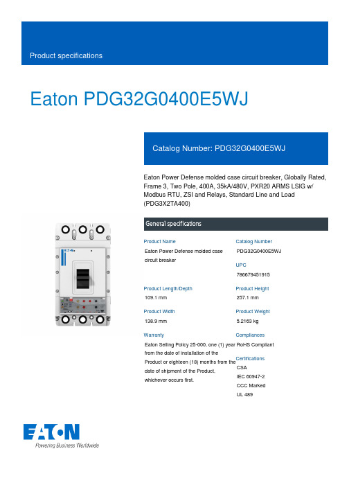
Eaton PDG32G0400E5WJEaton Power Defense molded case circuit breaker, Globally Rated, Frame 3, Two Pole, 400A, 35kA/480V, PXR20 ARMS LSIG w/ Modbus RTU, ZSI and Relays, Standard Line and Load (PDG3X2TA400)General specificationsEaton Power Defense molded case circuit breakerPDG32G0400E5WJ 786679451915109.1 mm 257.1 mm 138.9 mm 5.2163 kg Eaton Selling Policy 25-000, one (1) year from the date of installation of theProduct or eighteen (18) months from thedate of shipment of the Product,whichever occurs first.RoHS Compliant CSAIEC 60947-2CCC MarkedUL 489Product NameCatalog Number UPCProduct Length/Depth Product Height Product Width Product Weight WarrantyCompliancesCertifications400 AComplete breaker 3Two-polePD3 Global Class A PXR 20 LSIG w/ARMSModbus RTU600 Vac600 VStandard Line and Load35 kAIC at 480 Vac 10 kAIC Icu @250 Vdc 65 kAIC @240V (UL)400 AEaton Power Defense MCCB PDG32G0400E5WJ 3D drawing Power Xpert Protection Manager x32Consulting application guide - molded case circuit breakers Power Xpert Protection Manager x64Amperage Rating Circuit breaker frame type Frame Number of poles Circuit breaker type Class Trip TypeCommunication Voltage rating Voltage rating - max TerminalsInterrupt rating Interrupt rating range Trip rating 3D CAD drawing packageApplication notesBrochuresStrandAble terminals product aidPower Defense technical selling bookletPower Defense molded case circuit breaker selection posterPower Defense brochureCatalogsMolded case circuit breakers catalogPower Xpert Release trip units for Power Defense molded case circuit breakersCertification reportsPDG3 45-400A CB reportPDG3 CSA certification 100-400aPDG3 CSA certification 250-600aPDG3 UL authorization 100-400aPDG3 UL authorization 250-600a TMTUPDG3B 450A-600A CB reportEU Declaration of Conformity - Power Defense molded case circuit breakersInstallation instructionsPower Defense Frame 1-2-3-4 IP door barrier assembly instructions - IL012278ENPower Defense Frame 3 interphase barrier - IL012229EN H03 Power Defense Frame 3 plug-in adapter installation instructions -IL012311ENPower Defense Frame 3 multi-tap terminal kit Cat NumPDG3X3(2)(4)TA6006W Instructions - IL012248ENPower Defense Frame 3 multi wire connector kit -PDG3X3(2)(4)TA4006W and PDG3X3(2)(4)TA4003W instructions-IL012247EN H01Power Defense Frame 4 locking devices and handle block instructions - IL012151ENPower Defense Frame 3 locking devices and handle block instructions - IL012150ENPower Defense Frame 3 handle mech direct rotary handle instructions - IL012111ENPower Defense Frame 3 reverse feed connector kit Cat NumPDG3X3(2)(4)TA400HRF instructions - IL012252ENPower Defense Frame 3 rear connection installation instructions -IL012300ENPower Defense Frame 3 terminal spreader assembly instructions -IL012301ENPower Defense Frame 2/3/4/5/6 voltage neutral sensor module wiringinstructions – IL012316ENPower Defense Frame 3 Breaker Instructions (IL012107EN).pdfPower Defense Frame 3 shunt trip UVR instructions - IL012140EN Power Defense Frame 3 extendable shaft rotary handle mech -IL012112ENPower Defense Frame 3 adapter kit installation instructions LZM3 to PD3 - IL012227ENPower Defense Frame 3 box terminal installation instructions -IL012299ENPower Defense Frame 3 multi-tap terminal kit Cat NumPDG3X3(2)(4)TA6006WSW instructions - IL012250ENPower Defense Frame 3 reverse feed connector kit Cat NumPDG3X3(2)(4)TA630RF instructions - IL012253ENPower Defense Frame 3 trip unit replacement instructions - IL012157EN Power Defense Frame 3 terminal kit Cat Num PDG3X3(2)(4)TA400RF instructions - IL012251ENPower Defense Frame 4 shunt trip UVR instructions - IL012129EN Power Defense Frame 3 Direct Rotary Handle Assy With Interlock Version Instructions (IL012139EN).pdfPower Defense Frame 3 Aux, Alarm, ST and UVR Animated Instructions.rh Power Defense Frame 3 finger protection assembly installation instructions - IL012279ENPower Defense Frame 4 reverse feed connector kit instructions for PDG4X3(2)(4)TA800RF instructions - IL012254ENInstallation videosPower Defense Frame 3 Handle Mech Variable Depth Rotary Handle Animated Instructions.rhPower Defense Frame 3 Shunt Trip_UVR Animated Instructions.pdf.rh Power Defense Frame 3 Handle Mech Direct Rotary Handle Animated Instructions.rhPower Defense Frame 3 trip unit replacement animated instructions.rh Power Defense Frame 3 Locking Devices and Handle Block Animated Instructions.pdf.rhMultimediaPower Defense Frame 3 Aux, Alarm, Shunt Trip, and UVR How-To Video Power Defense Frame 5 Trip Unit How-To VideoPower Defense Frame 3 Variable Depth Rotary Handle Mechanism Installation How-To VideoPower Defense Frame 6 Trip Unit How-To VideoPower Defense Frame 2 Variable Depth Rotary Handle Mechanism Installation How-To VideoPower Defense molded case circuit breakersEaton Corporation plc Eaton House30 Pembroke Road Dublin 4, Ireland © 2023 Eaton. All Rights Reserved. Eaton is a registered trademark.All other trademarks areproperty of their respectiveowners./socialmediaEaton Power Defense for superior arc flash safety Power Defense Breakers Eaton Specification Sheet - PDG32G0400E5WJ Power Defense time current curve Frame 3 - PD3Intelligent circuit protection yields space savings Single and double break MCCB performance revisited Intelligent power starts with accurate, actionable data Making a better machineMolded case and low-voltage power circuit breaker healthImplementation of arc flash mitigating solutions at industrial manufacturing facilitiesMolded case and low-voltage breaker health Safer by design: arc energy reduction techniquesSpecifications and datasheetsTime/current curvesWhite papers。
PMEM4020APD,115;中文规格书,Datasheet资料
1.Product profile1.1General descriptionCombination of a PNP transistor with low V CEsat and high current capability and a planar Schottky barrier rectifier with an integrated guard ring for stress protection in a SOT457(SC-74) small plastic package. NPN complement: PMEM4020AND1.2FeaturesI 600 mW total power dissipation I High current capability up to 2 AI Reduces printed-circuit board area required I Reduces pick and place costs I Small plastic SMD package ITransistorN Low collector-emitter saturation voltage I DiodeN Ultra high-speed switching N Very low forward voltage N Guard ring protected1.3ApplicationsI DC-to-DC converters I Inductive load driversI General purpose load driversI Reverse polarity protection circuits IMOSFET drivers1.4Quick reference dataPMEM4020APDPNP transistor/Schottky rectifier moduleRev. 02 — 31 August 2009Product data sheetTable 1.Quick reference data Symbol ParameterConditions Min Typ Max Unit PNP transistorV CEO collector-emitter voltage open base --−40V I Ccollector current (DC)continuous;T s ≤ 55°C[1]--−2A[1]Soldering point of collector or cathode tab.2.Pinning information3.Ordering information4.Marking5.Limiting valuesSchottky barrier rectifierV R continuous reverse voltage --40V I Fcontinuous forward current--1ATable 1.Quick reference data …continued Symbol ParameterConditionsMin Typ Max Unit Table 2.Discrete pinningPin Description Simplified outline Symbol1emitter 2not connected 3cathode 4anode 5base 6collector132456sym04036145Table 3.Ordering informationType numberPackage NameDescriptionVersion PMEM4020APDSC-74plastic surface mounted package; 6 leadsSOT457Table 4.MarkingType number Marking code PMEM4020APDD3Table 5.Limiting valuesIn accordance with the Absolute Maximum Rating System (IEC 60134).Symbol ParameterConditions Min Max Unit PNP transistorV CBO collector-base voltage open emitter -−40V V CEO collector-emitter voltage open base -−40V V EBOemitter-base voltageopen collector-−5V[1]Mounted on a FR4 printed-circuit board, single-sided copper, tin-plated, standard footprint.[2]Device mounted on a printed-circuit board, single-sided copper, tin-plated, 1cm 2 mounting pad for both collector and cathode.[3]Mounted on a ceramic printed-circuit board, single-sided copper, tin-plated, standard footprint.[4]Soldering point of collector or cathode tab.I Ccollector current (DC)continuous [1]-−0.75A continuous [2]-−1A continuous [3]-−1.3A continuous;T s ≤ 55°C[4]-−2A I CM peak collector current -−3A I BM peak base current -−1A P tottotal power dissipationT amb ≤ 25°C [1]-295mW T amb ≤ 25°C [2]-400mW T amb ≤ 25°C [3]-500mW T s ≤ 55°C[4]-1000mW T j junction temperature -150°C Schottky barrier rectifierV R continuous reverse voltage -40V I F continuous forward voltage -1A I FRM repetitive peak forward currentt p ≤ 1 ms;δ≤ 0.5- 3.5A I FSM non-repetitive peak forward currentt = 8 ms; square wave -10A P tottotal power dissipationT amb ≤ 25°C [1]-295mW T amb ≤ 25°C [2]-400mW T amb ≤ 25°C [3]-500mW T s ≤ 55°C[4]-1000mW T j junction temperature [2]-150°C Combined deviceP tot total power dissipation T amb ≤ 25°C[2]-600mW T stg storage temperature −65+150°C T ambambient temperature[2]−65+150°CTable 5.Limiting values …continuedIn accordance with the Absolute Maximum Rating System (IEC 60134).Symbol ParameterConditions Min Max Unit6.Thermal characteristics[1]For Schottky barrier rectifiers thermal run-away has to be considered, as in some applications the reverse power losses P R are a significant part of the total power losses. Nomograms for determining the reverse power losses P R and I F(AV) rating will be available on request.[2]Soldering point of collector or cathode tab.[3]Mounted on a ceramic printed-circuit board, single-sided copper, tin-plated, standard footprint.[4]Device mounted on a printed-circuit board, single-sided copper, tin-plated, 1cm 2 mounting pad for both collector and cathode tab.[5]Mounted on a FR4 printed-circuit board, single-sided copper, tin-plated, standard footprint.Table 6.Thermal characteristics [1]Symbol Parameter Conditions Min Typ Max Unit Single device R th(j-s)thermal resistance from junction to soldering point in free air [2]--95K/W R th(j-a)thermal resistance from junction to ambientin free air[3]--250K/W [4]--315K/W [5]--425K/W Combined device R th(j-a)thermal resistance from junction to ambientin free air[3]--208K/W7.Characteristics[1]Pulse test: t p ≤ 300µs;δ≤ 0.02Table 7.CharacteristicsT amb = 25°C unless otherwise specified Symbol ParameterConditionsMin Typ Max Unit PNP transistorI CBOcollector-base cut-off current V CB =−40 V; I E = 0 A --−100nA V CB =−40 V; I E = 0 A;T j = 150°C--−50µA I CEO collector-emitter cut-off current V CE =−30 V; I B = 0 A --−100nA I EBO emitter-base cut-off current V EB =−5 V; I C = 0 A --−100nAh FEDC current gainV CE =−5 V; I C =−1 mA 300--V CE =−5 V; I C =−100 mA 300--V CE =−5 V; I C =−500 mA 250-900V CE =−5 V; I C =−1 A 160--V CE =−5 V; I C =−2 A[1]50--V CEsatcollector-emitter saturation voltageI C =−100 mA; I B =−1 mA --−120mV I C =−500 mA; I B =−50 mA --−145mV I C =−1 A; I B =−100 mA --−260mV I C =−2 A; I B =−200 mA--−530mV R CEsat equivalent on-resistance I C =−1 A; I B =−100 mA [1]-180280m ΩV BEsat base-emittersaturation voltage I C =−1 A; I B =−100 mA [1]--−1.1V V BEon base-emitter turn-on voltageV CE =−5 V; I C =−1 A [1]--−1.0V f T transition frequency V CE =−10 V; I C =−50 mA;f = 100 MHz150--MHz C ccollector capacitanceV CB =−10 V; I E = i e = 0 A;f = 1 MHz --10pFSchottky barrier rectifier V Fcontinuous forward voltagesee Figure 1I F = 0.1 mA [1]-95130mV I F = 1 mA [1]-155210mV I F = 10 mA [1]-220270mV I F = 100 mA [1]-295350mV I F = 1000 mA[1]-540640mV I Rreverse currentsee Figure 2V R = 10 V [1]-720µA V R = 40 V[1]-30100µA C ddiode capacitanceV R = 1 V; f = 1 MHz;see Figure 3-4348pFSchottky barrier rectifier (1)T amb =150°C (2)T amb =85°C (3)T amb =25°CSchottky barrier rectifier (1)T amb =150°C (2)T amb =85°C (3)T amb =25°CFig 1.Forward current as a function of forward voltage; typical valuesFig 2.Reverse current as a function of reverse voltage; typical valuesSchottky barrier rectifier;T amb = 25°C; f = 1 MHzPNP transistor;V CE =−5 V (1)T amb = 150°C (2)T amb = 25°C (3)T amb =−55°CFig 3.Diode capacitance as a function of reverse voltage; typical valuesFig 4.DC current gain as a function of collector current; typical values0.60.40.2010310210110−1mdb669I F (mA)V F (V)(1)(2)(3)020103040V R (V)mdb670105104103102101I R (µA)(1)(2)(3)05102010008015604020mdb671V R (V)C d (pF)012002004006008001000mhc088−10−1h FE −10−1I C (mA)−102−103−104(1)(2)(3)PNP transistor;V CE =−5 V (1)T amb =−55°C (2)T amb = 25°C (3)T amb = 150°CPNP transistor;I C /I B = 10(1)T amb = 150°C (2)T amb = 25°C (3)T amb =−55°CFig 5.Base-emitter voltage as a function of collector current; typical valuesFig 6.Collector-emitter saturation voltage as a function of collector current; typical valuesPNP transistor;I C /I B = 10(1)T amb = 150°C (2)T amb = 25°C (3)T amb =−55°CPNP transistor;V CE =−10 VFig 7.Equivalent on-resistance as a function of collector current; typical valuesFig 8.Transition frequency as a function of collector current−10−1−10−1mhc089−10−1−1−10V BE (V)I C (mA)−103−102−104(1)(2)(3)−103−102−10−1mhc090−1−10V CEsat (mV)I C (mA)−102−103−104(1)(2)(3)10110−1102mhc091−10−1−1−10R CEsat (Ω)I C (mA)−103−102−104(1)(2)(3)0−100030010020025050150−200−400f T (MHz)I C (mA)−600−800mhc0928.Application informationFig 9.DC-to-DC converterFig 10.Inductive load driver (relays, motors andbuzzers) with free-wheeling diodemgu866V OUTV INCONTROLLERmgu867V CCIN9.Package outlineFig 11.Package outline SOT457 (SC-74)REFERENCESOUTLINE VERSION EUROPEAN PROJECTIONISSUE DATE IECJEDECJEITA SOT457SC-74w BM b pD epin 1indexAA 1L pQdetail XH EE v M AA B yscalecX13245601 2 mmPlastic surface-mounted package (TSOP6); 6 leadsSOT457UNIT A 1b p c D E H E L p Q y w v mm0.10.0130.400.253.12.70.260.101.71.3e 0.953.02.50.20.10.2DIMENSIONS (mm are the original dimensions)0.60.20.330.23A 1.10.905-11-0706-03-1610.Packing informationTable 8.Packing methodsThe indicated -xxx are the last three digits of the 12NC ordering code.[1]Type number Package Description Packing quantity300010000 PMEM4020APD SOT457 4 mm pitch, 8 mm tape and reel; T1-115-1354 mm pitch, 8 mm tape and reel; T2-125-165 [1]For further information and the availability of packing methods, see Section13.分销商库存信息: NXPPMEM4020APD,115。
APD3224PBCA-F01;中文规格书,Datasheet资料

Notes: 1.Wavelength: +/-1nm. 2. Forward Voltage: +/-0.1V.
Absolute Maximum Ratings at TA=25°C
Parameter Power dissipation DC Forward Current Peak Forward Current [1] Reverse Voltage Operating Temperature Storage Temperature
3.2x2.4mm SMD CHIP LED LAMP
Part Number: APD3224PBC/A-F01 Blue
ATTENTION
OBSERVE PRECAUTIONS FOR HANDLING ELECTROSTATIC DISCHARGE SENSITIVE DEVICES
Features
Description
The Blue source color devices are made with InGaN on SiC Light Emitting Diode. Static electricity and surge damage the LEDS. It is recommended to use a wrist band or anti-electrostatic glove when handling the LEDs. All devices, equipment and machinery must be electrically grounded.
Note: 1. 1/10 Duty Cycle, 0.1ms Pulse Width.
Blue 120 30 100 5 -40°C To +85°C -40°C To +85°C
APD-320G064中文资料
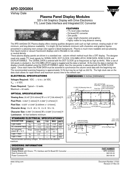
320 x 64 Full Field Pixel Pitch: 0.066 [1.68] Vertical 0.064 [1.63] Horizontal 0.148 [3.76] Mountng Holes (8) Pixel Size: 0.040 [1.02] Diameter 0.40 21.616 [549.05] [10.16] 5.478 4.198 5.778 [139.14] [106.63] [146.76] 0.150 [3.81] 0.54 [13.72] 0.83 0.150 [21.08] [3.81]
1.30 [33.02] Max. Pin #1 of P2 0.800 [20.32] Max. Component Height
....... ....... ....
0.35 ± 0.02 [8.89 ± 0.51]
Vil * Recommended operating voltages. All maximums are absolute maximum.
FEATURES
• TTL level video interface • On board DC converter • Slim profile • Large, bright characters and graphics • Highly visible for long distance viewing The APD-320G064 DC Plasma display offers viewing qualities designers seek such as high contrast, viewing angle of 150° minimum, and long distance readability. It is bright (50 foot lamberts minimum) with characters and graphics figures presented in a pleasing neon orange color against a black background. Plasma is much more readable and eye-pleasing than liquid crystal or vacuum fluorescent displays and is filterable to red, amber, or neutral density. These plasma display panels are driven in a standard row - column refresh method much like a CRT display. The designer need only supply TTL level signals for SERIAL DATA, DOT CLOCK, COLUMN LATCH, ROW DATA, ROW CLOCK and DISPLAY ENABLE. The SERIAL DATA is entered with the DOT CLOCK up to frequencies as high as 8mHz. After a row of 320 pixels is clocked in, the COLUMN LATCH signal is toggled and the data is latched. At the time the data is latched, the display is briefly disabled using the DISPLAY ENABLE signal, then the row pointer is advanced with the ROW CLOCK signal. Once each frame the ROW DATA must be asserted to synchronize the column serial data with the beginning row. The recommended scanning frequency is approximately 70 Hz but may be as high as 200 Hz. The high clock rate on the data clock allows for rapid refresh and maximum access time to the refresh ram.
- 1、下载文档前请自行甄别文档内容的完整性,平台不提供额外的编辑、内容补充、找答案等附加服务。
- 2、"仅部分预览"的文档,不可在线预览部分如存在完整性等问题,可反馈申请退款(可完整预览的文档不适用该条件!)。
- 3、如文档侵犯您的权益,请联系客服反馈,我们会尽快为您处理(人工客服工作时间:9:00-18:30)。
3.2x2.4mm SMD CHIP LED LAMP
APD3224PBC BLUE
Features
!3.2x2.4mm SMT LED, 2.4mm THICKNESS. !LOW POWER CONSUMPTION. !IDEAL FOR BACKLIGHT AND INDICATOR. !VARIOUS COLORS AND LENS TYPES AVAILABLE. !PACKAGE : 1500PCS / REEL.
PAGE: 4 OF 4
Absolute Maximum Ratings at T)=25°C °
Par am et er Power dissipation DC Forward Current Peak Forward Current [1] Reverse Voltage Operating /Storage Temperature
SPEC NO: DSAB2587 APPROVED : J. Lu
REV NO: V.3 CHECKED :Allen Liu
DATE:MAR/22/2003 DRAWN:D.L.HUANG
PAGE: 1 OF 4
元器件交易网
Selection Guide
Par t No . Dic e L en s Ty p e Iv (m c d ) @20m A Min . A P D 3 2 2 4P B C BLUE ( InGaN) WATER CLEAR 180 Ty p . 450 V i ew i n g An g l e 2θ1/2 20 °
DATE:MAR/22/2003 DRAWN:D.L.HUANG
PAGE: 2 OF 4
元器件交易网
Blue
APD3224PBC
SPEC NO: DSAB2587 APPROVED : J. Lu
REV NO: V.3 CHECKED :Allen Liu
DATE:MAR/22/2003 DRAWN:D.L.HUANG
Note: 1. θ1/2 is the angle from optical centerline where the luminous intensity is 1/2 the optical centerline value.
° Electrical / Optical Characeak λD ∆λ1/2 C VF IR Par am et er Peak Wavelength Dominate Wavelength Spectral Line Half-width Capacitance Forward Voltage Reverse Current Blue Blue Blue Blue Blue Blue D ev i c e Ty p . 468 470 25 65 3.65 4.2 10 Max . Un it s nm nm nm pF V uA Tes t Co n d it io n s I F =20mA I F =20mA I F =20mA VF = 0V;f=1MHz I F =20mA V R = 5V
PAGE: 3 OF 4
元器件交易网
APD3224PBC SMT Reflow Soldering Instructions
Number of reflow process shall be less than 2 times and cooling process to normal temperature is required between first and second soldering process.
Recommended Soldering Pattern (Units : mm)
Tape Specifications (Units : mm)
SPEC NO: DSAB2587 APPROVED : J. Lu
REV NO: V.3 CHECKED :Allen Liu
DATE:MAR/22/2003 DRAWN:D.L.HUANG
Description
The Blue source color devices are made with InGaN on SiC Light Emitting Diode.
Package Dimensions
Notes: 1. All dimensions are in millimeters (inches). 2. Tolerance is ±0.1(0.004") unless otherwise noted. 3. Specifications are subject to change without notice.
Note: 1. 1/10 Duty Cycle, 0.1ms Pulse Width.
B lu e 10 2 30 160 5 -40°C To +85°C
Un it s mW mA mA V
SPEC NO: DSAB2587 APPROVED : J. Lu
REV NO: V.3 CHECKED :Allen Liu