基于SPARC结构的RISC系统设计技术
sparc V8嵌入式体系结构

36
9. 1处理器状态寄存器 (Processor State Register) PSR
11
4.芯片描述(IU)
指令时序:S698_ECR 的指令按照功能分为6 类: 存储器存取指令、算术运算/逻辑运算/移位指令、 跳转控制指令、读/写寄存器指令、浮点运算指令 和其它指令。
12
4.芯片描述(IU)
存储器存取指令 存储器存取指令是唯一用来访问存储器的指令。 存储器存取指令用2个‘r’寄存器或者1个‘r’寄 存器和1个13-bit的无符号立即数计算出1个32bit、按字节排列的存储器地址,IU再在该地址 后面加上“地址空间标志符(ASI)”以决定处 理器是处于管理模式还是用户模式,是访问指令 存储器还是数据存储器。
2
2 .特点
基于AMBA 总线的可裁减结构: S698_ECR内部的AMBA总线包括2种总线: AHB和APB。APB总线用来访问片内外设的寄存器; AHB总线用作高速数据传输。
3
2 .特点
高性能的处理器内核(带有4K 字节的指令cache 和4K 字节的数据cache) 32-bit整型数处理单元 RISC结构 硬件乘法器和除法器 5级流水 优化的32/64-bit浮点数处理单元,符合 IEEE-754标准
15
4.芯片描述(IU)
S698对半字的大于一个字节类型的数据采用高地 址优先存储的方式。
16
4.芯片描述(IU)
算术运算/逻辑运算/移位指令 算术运算/逻辑运算/移位指令提供了算术运算、 逻辑运算和移位操作。这些指令除“SETHI”指令 之外,都包括2个操作码,并由这2个操作码运算 产生一个结果,这个结果或者放入目的寄存器中, 或者丢弃。“SETHI”指令是一条专门的指令,用 来和它后面的指令一起创建一个32位的常数并放 入r寄存器中。
risc-v 边缘计算

risc-v 边缘计算RISC-V是一种基于精简指令集(Reduced Instruction Set Computing,RISC)的开源指令集架构(Instruction Set Architecture,ISA)。
它的设计灵感主要来自于经典的RISC ISA,如MIPS和SPARC。
RISC-V指令集是简单、模块化和可扩展的,可以适应从微控制器到大型服务器的各种应用场景。
边缘计算是一种新兴的计算模型,旨在将数据处理和存储与数据源更接近的地方进行,以减少数据传输延迟和网络拥塞。
传统的计算模型将大量的数据发送到云端进行处理,然而,随着物联网和大数据应用的普及,这种模型已经显得低效且不可持续。
因此,边缘计算在解决这一问题上发挥了重要作用。
RISC-V和边缘计算之间存在着天然的互补关系。
首先,由于RISC-V指令集的简洁和可扩展性,它非常适合在边缘设备上进行实现。
边缘设备的计算能力通常有限,因此需要一种高效且灵活的指令集架构来实现各种计算任务。
RISC-V的设计理念正与此相符合。
其次,RISC-V的开源性使得开发者可以自由地对其进行修改和定制,以适应不同的边缘计算应用场景。
边缘计算的特点是具有高度的异构性,不同的边缘设备可能需要不同的计算资源和指令集扩展。
而RISC-V的开源性为开发者提供了更大的自由度,可以根据具体需求进行定制化。
此外,RISC-V的开放生态系统也为边缘计算提供了更多的可能性。
开源的设计模式使得RISC-V能够更加容易被整合到已有的边缘计算平台中。
从硬件角度来看,边缘设备的资源通常有限,而RISC-V基于模块化的设计使得它可以在不同的硬件平台上进行裁剪和优化。
从软件角度来看,RISC-V的开源体系使得开发者能够更加灵活地开发和优化边缘计算的应用程序。
除此之外,RISC-V还具备较低的能耗和更好的性能。
边缘计算的一个重要特征是设备在离线模式下需要更长的续航时间,而低能耗是实现这一目标的重要因素之一。
ASIC、NP、X86、RISC、DSP 、ARM、单片机几种常见技术介绍
RISC微处理器不仅精简了指令系统,采用超标量和超流水线结构;它们的指令数目只有几十条,却大大增强了并行处理能力。如:1987年Sun
Microsystem公司推出的SPARC芯片就是一种超标量结构的RISC处理器。而SGI公司推出的MIPS处理器则采用超流水线结构,这些RISC处理器在构建并行精简指令系统多处理机中起着核心的作用。
(2)程序和数据空间分开,可以同时访问指令和数据;
(3)片内具有快速RAM,通常可通过独立的数据总线在两块中同时访问;
(4)具有低开销或无开销循环及跳转的硬件支持;
(5)快速的中断处理和硬件I/O支持;
● 分级存储器组织: NP存储器一般包含多种不同性能的存储结构,对数据进行分类存储以适应不同的应用目的。
● 高速I/O接口:
NP具有丰富的高速I/O接口,包括物理链路接口、交换接口、存储器接口、PCI总线接口等。通过内部高速总线连接在一起,提供很强的硬件并行处理能力。
现代ASIC常包含整个32-bit处理器,类似ROM、RAM、EEPROM、Flash的存储单元和其他模块.
这样的ASIC常被称为SoC(片上系统)。
FPGA是ASIC的近亲,一般通过原理图、VHDL对数字系统建模,运用EDA软件仿真、综合,生成基于一些标准库的网络表,配置到芯片即可使用。它与ASIC的区别是用户不需要介入芯片的布局布线和工艺问题,而且可以随时改变其逻辑功能,使用灵活。
针对滤波、相关、矩阵运算等需要大量乘和累加运算的特点,DSP的算术单元的乘法器和加法器,可以在一个时钟周期内完成相乘、累加两个运算。近年出现的某些DSP如ADSP2106X、DSP96000系列DSP可以同时进行乘、加、减运算,大大加快了FFT的蝶形运算速度。
S698MIL-DKit S698-MIL 芯片应用开发系统 使用说明书

S698MIL-DKitS698-MIL芯片应用开发系统使用说明书V 3.2珠海欧比特控制工程股份有限公司 地址:广东省珠海市唐家东岸白沙路1号欧比特科技园邮编:519080 电话*************传真*************网址:S698-MIL芯片应用开发系统(S698MIL-DKit)使用说明书前言本说明书是S698-MIL芯片应用开发系统(S698MIL-DKit)使用说明书。
本开发系统使用的是SAILING S698-MIL处理器(以下简称S698-MIL处理器)是针对嵌入式实时控制及信息处理应用而研制的32位RISC嵌入式处理器,其设计遵循SPARC V8标准。
SPARC是国际上流行的处理器架构之一,在业内享有盛名,具备广大的用户群和广阔的应用领域。
S698-MIL是高性能的、SPARC V8架构的、32-bit RISC嵌入式微处理器,采用0.18 µm CMOS工艺制造,QFP160封装。
S698-MIL内部采用AMBA总线,内嵌32-bit整型数处理单元(包括4K字节的指令cache 和4K字节的数据cache),优化的32/64-bit浮点数处理单元,具有较强的运算能力;并且内嵌了大量的外设,主要包括:80-bits GPI口、4路UART接口、5个24-bits定时器、实时时钟、看门狗、PS/2接口、I2C总线接口、SPI总线接口、1个三磁道磁卡接口,3个智能卡接口等;另外,还内嵌了带有后备电源的、32K字节的RAM,掉电时可保存数据不致丢失。
S698-MIL是专为税控收款机、银行POS机等终端设备量身定做的一块微处理器。
S698-MIL内嵌有功能强大的调试单元DSU,DSU对外接口是一个普通的UART串口,通过DSU口,用户可以访问CPU内部所有寄存器和存储器资源,也可访问外部所有存储器和I/O外设,使硬件/软件调试变得极为方便。
S698-MIL支持标准C语言编写的程序,而且也支持ORBITA实时嵌入式操作系统ORBITA EOS,还支持实时嵌入式操作系统RTEMS及嵌入式操作系统uClinux。
SPARC V8处理器基于PC 104嵌入式计算机模块设计说明书
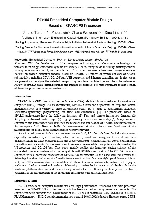
Joint International Mechanical, Electronic and Information Technology Conference (JIMET 2015)PC/104 Embedded Computer Module DesignBased on SPARC V8 ProcessorZhang Tong1,2, a *, Zhou Jiqin3,b,Zhang Weigong2,3,c , Ding Lihua1,2,d1College of Information Engineering, Capital Normal University, Beijing, 100048, China2Beijing Engineering Research Center of High Reliable Embedded System, Beijing, 100048, China 3Beijing Center for Mathematics and Information Interdisciplinary Sciences, Beijing, 100048, China a*****************,b******************,c*************,d****************Keywords: Embedded Computer, PC/104, Domestic processor, SPARC V8Abstract: With the development of the computer technology, microelectronics technology and network technology, embedded-systems are widely used in many fields including industry control, railway locomotive control, and vehicle, etc. This paper proposes a hardware design scheme of PC/104 embedded computer module based on SPARC V8 processor which consists of several sub-modules including CPU , PC/104 bus, USB controller and Ethernet controller, etc. In this paper, we present and analyze the detailed design of system level architecture and the sub-modules of PC/104 module. It has a certain reference and guidance significance to further promote the application of domestic processor in various industries.IntroductionSPARC is a CPU instruction set architecture (ISA), derived from a reduced instruction set computer (RISC) lineage. As an architecture, SPARC allows for a spectrum of chip and system implementations at a variety of price/performance points for a range of applications, including scientific/engineering, programming, real-time, and commercial [2]. The processors based on SPARC architecture have the following features: (1) Few and simple instruction formats. (2) Adopting hard-wired control logic. (3) High processing capacity and reliability [6]. Many domestic companies and universities have launched the research and application of SPARC microprocessor in the aerospace field. How to build the environment of the software and hardware of the microprocessors based on this architecture is worthy studying.As a kind of common industrial computer bus standard, PC/104 is defined for industrial control especially embedded system control, which is mostly used for management control and data transmission in the fields of aeronautical and space because of its small size, low power consumption and software universality. So it is significant to research the embedded computer module based on the V8 processor and PC/104 bus. This paper mainly studies the hardware design scheme of the embedded computer module which is compatible with PC/104 specification. The PC/104 module is equipped with a domestic processor of SPARC V8 architecture as the CPU and implements the following functions including the friendly human-machine interface, the high-speed data acquisition unit, the USB communication sub-module and Ethernet communication sub-module. In this paper, we have applied structured and modular philosophy to design the hardware, which leads to brisk the hardware platform structure and makes it easy to extend or cut. It can provide a general hardware platform for the development of the intelligent instrument with different functions.Structure DesignPC/104 embedded computer module uses the high-performance embedded domestic processor based on the SPARC V8 architecture, which has been applied in many aerospace products. The computer module supports the 16/8 bit mode of PC/104 bus. It contains a 128MB SDRAM, a 128MB FLASH memory, 4 RS232 serial communication ports, 2 10M/100M adaptive Ethernet ports, 2 USBports and a VGA display port with 1600*1200 display resolution. In this PC/104 module, we have configured VxWorks operating system including BSP, USB keyboard mouse driver, Ethernet driver, UART driver, TFFS file system and other software driver [1]. Drivers are designed for the corresponding hardware devices, such as USB, Ethernet, UART and display control circuit to manage the underlying hardware, which can provide a standardized and hardware-independent interface to the high-level application software. Fig. 1 shows the main block diagram of PC/104 embedded computer module.Fig. 1 The main block diagram of PC/104 embedded computer moduleHardware Module Design Based on Domestic ProcessorCPU Sub-module A 32-bit microprocessor based on SPARC V8 architecture with the high degree of integration and high performance is adopted in this design. Fig. 2 shows the internal structure of the processor. From Fig. 2, we can see the processor chip contains an on-chip integer processing unit IU, a floating-point unit (FPU), independent data caches and instruction caches, 5 stage pipeline, hardware multiplier and divider and so on. Moreover, interrupt controller, hardware debug unit with tracking buffer storage (DSU), two common timer (timer0, timer1), serial interface, PCI interface, watchdog timer and memory controller supporting PROM, SRAM, SDRAM and I/O space accessing and so on are integrated in this processor chip[4].Fig. 2 The structure diagram of SPARC V8 CPUPC/104 Bus Sub-module The electrical logic of PC/104 specification uses ISA bus specification. It defines two types ofaddress space including I/O space and memory space, supporting 8-bit and 16-bit data accessing. The hardware of PC/104 can configure 11 interrupt sources and provide 7 DMA Channels. Due to the characteristics of V8 processor chip, in the designing of PC/104 module, we use dual space mapping mode to support the 8/16 read-write functions of PC/104 bus. The I/O space of V8 processor has the following two regions:(1) One region is used to deal with the 16-bit read-write functions of PC/104 bus, which can be divided into two subspaces, namely I/O space and memory space. The PC/104 bus accessing operations to this space are all considered to be 16-bit read-write mode. In this region, the MEMCS16# and IOCS16# signals are all ignored (assuming the device accessed is 16 bits).(2) Another region is specifically designed for 8-bit read-write functions of PC/104 bus, which can also be divided into two subspaces, namely IO space and storage space. The PC/104 bus accessing operations to this space are considered to be 8-bit read-write mode. The accessed device is served as an 8-bit device or a 16-bit device by the MEMCS16# and IOCS16# signal and the PC/104 data bus is mapped into the corresponding space of the processor.In order to improve the efficiency of bus accessing and the controlling flexibility, we implement the bus sequential control logic circuits on a FPGA chip. Through this designing method, the PC/104 bus sequence can be set flexibly by configuring the software, for example, the length (T1) of the address latch signal (BALE) or the default length (T2) of the bus access cycle can be changed by modifying the control register. The PC/104 bus sequence waveforms are shown in Fig. 3. In this figure, the term T4 is the time gap between the BALE falling edge and read-write signal falling edge, which has a minimum value of zero.As shown in Fig. 3, the length of T1 can be set by the BALEW domain of PC/104 bus sequence control register (ISATIMING). The length of T4 is 0~10ns. The length of T3 is T2-T1-T3. The default value of T2 is set by the ISAW domain of ISATIMING register.Fig. 3 PC/104 bus waveform DiagramUSB Sub-module In this paper, we use CH374U (produced by Nanjing QinHeng Electronics Co.,Ltd.) as the USB controller of PC/104 embedded computer module and implement two USB1.0 ports (usb0, usb1), which can connect keyboard, mouse, or the other USB external devices. The interface of USB adopts PulseGuard ESD protection circuit to implement the over-voltage protection. CH374U supports both USB-HOST and USB-DEVICE mode with root hub of 3 ports. It has multiple transmission method, including low speed and full speed control transmission, bulk transmission, interrupt transmission, and synchronous transmission. CH374U uses four I/O registers to interact with the CPU and can generate an interrupt request to CPU. The four registers are all adopted 16-bit accessing mode, but only low 8 bits are effective. High 8 bits are read with constant zero and writing in is arbitrary. The hardware block diagram of USB is shown in Fig. 4.Fig. 4 USB signal connection diagramEthernet Sub-module The two-way 10M/100M adaptive Ethernet interface (LAN1, LAN2) is implemented with the module using DM9000CIEP owned by Davicom Semiconductor, Inc. In order to improve the reliability of the internal work of the PC/104 embedded computer module, the double isolation interface scheme is adopted in the Ethernet interface, namely the input and output signals separated by the transformer. Two way Ethernet interfaces can work independently and also can be redundant backup for each other used under the driver management [5]. The hardware block diagram is shown in Fig. 5.ADRESSBALER/WIOCHRDYRead DataWrite DataFig. 5 Ethernet signal connection DiagramTest resultsThe cast plate is made according to the above design and the module real figure is shown in Fig. 6. The PCB boards are put to the test and the tests are mainly about the validity of the various functions modules of the PC/104 embedded computer module. The tests are mainly as follows:Fig. 6 Module physical Diagram(1) CPU functional testing, the main function is to test the cache, perform the same cycle, it is 19us to open the cache code, 195us to close the cache code time.(2) In order to test the PC/104 module more fully, we design a motherboard with a CPLD chip which implements several registers including ISA bus interrupt request control register, accessing latency control register, clock-timing registers.The V8 PC/104 computer module can access these functional registers by internal ISA bus in order to control the CPLD to generate the bus interrupts or modify the bus latency. Using these control method, we can implement the test of PC/104 module.The generation and clear of the PC/104 bus interrupt signal is controlled by the interrupt request register and the interrupt enable register, which is how the bus interrupt signal is tested.The bus access cycle controller is mainly to test the validity of the bus access after inserting the different length of wait states the maximum of which is 256us. These waiting for the cycle controllers is only effective for testing the functional registers (IO address 0000 ~ 00FFH). The signal IOCHRDY is in the state of high resistance and the default cycle is adopted while the registers are accessed by other ISA address.The timer is set with a kind of bus clock when the clock timing is tested. And firstly the 33MHz (CPLD operating clock), 14.318MHz (bus BCLK clock), 14.318MHz (bus OSC clock) are respectively divided into 1MHz by an internal frequency divider, and then the signal is stipulated-timing-controlled by a set of registers. When it comes to overflowing in the timer, the interrupt request is applied to the ISA bus by the interrupt request signal (IRQ12, 14 or 15). And the timer can be tested by software reading the timer count.(3) Ethernet communication test: Two way Ethernet are connected to the test monitoring computer with the router. Ethernet transferring the data is normal and the average transfer rate is about 1Mbps, and the error rate is zero, and the packet loss rate is zero.(4) In the operating system, SDRAM memory which is not occupied by the operating system is accessing tested. In order to accurately test the validity of the data bus, writing-in data must have wide adaptability, including 0x55555555、0xaaaaaaaa、0x1、0x2、0x4、0x8、0x10、……、0x80000000. The data in two formats is mainly tested for reading the preliminarily stored data in the FLASH memory. One is the binary data stored in the space that is not changed into the file system, the other is a file stored in the file system, and the test results are correct. Display images and memory access test: After receiving the test command, the specific graphics display functions are called so that the specific graphics can be displayed on the display and the read and write accessing to the display buffer memory is normal. In the RS232 communication test, four RS232 interfaces of the V8 PC/104 computer module are two-two interconnected to send and receive data, and serial data transmission is normal, and the average Baud rate is about 90kbps, and the error rate is zero.ConclusionsThe embedded system has been widely used in the field of industrial control, such as industrial process control, intelligent instrument, and numerical control system. Especially with the network technology and communication technology rapidly booming, the networked site of the industrial control has become a trend. In this paper, after studying the development situation of the embedded system at home and abroad, the relatively complete solution to the embedded application system is designed with a high-performance domestic embedded processor based on SPARC V8 architecture. And the 128MB bytes of FLASH that is used to store all the program codes and parameters is extended in this system and the 128MB bytes of SDRAM that is used to store running programs and data is extended in this system and PC/104 bus is extended in this system to improve the efficiency of bus access and control flexibility. Moreover, USB, Ethernet communication interface and etc. are designed in this system. The testing results indicate that the function indexes and performance indexes meet the requirements. This module is featured in a small size, powerful functions, low power consumption, high reliability, good compatibility and low cost [3], which means it can be applied in different fields of the industrial occasions.AcknowledgmentsThis work was supported in part by the National Natural Science Foundation of China (No.61170009, No.61472260, No.61402302); Beijing Natural Science Foundation of China (No.4132016, No.4143060); the Project of Construction of Innovative Teams and Teacher Career Development for Universities and Colleges Under Beijing Municipality(No.IDHT20150507); the Scientific Research Base Development Program of the Beijing Municipal Commission of Education. References[1] Zhang Lihong, Ren Yu, Chen Jianzheng, Data Acquisition System Based On PC/104, Engineering and Test,2009,3[2] The SPARV Architecture Manual, Version 8[3] Cao Zhijin, Hou Xia, Wu Qiuping, Master-slave data acquisition systems and applications based on PC/104,Electrical Measurement and Instrumentation, 2003,4[4] Yu Dan, Zhang Zhuancheng, Feng Lijie, Lai Yuqiang, LEON2 processor-based SoC designs based on LEON2 processor, Modern electronic technology, 2005[5] Chen Yi, Wang Lei, Zhou guojia, Li Zhe, Radiation Monitoring Network and Ethernet Interface Based On CAN bus, Nuclear Electronics and Detection Technology,2011[6] Zhu Xiaoyan, Zhang Weigong, Wang Jianfeng, Duan Qingya, and Liu Shurong, “The design of high reliable serial system BUS”. Proceedings of Computer Design and Applications, Qinhuangdao,Hebei, China, 25-27 June 2010; pp.V4-14-V4-17.。
RISC和CISC的区别
RISC和CISC的区别RISC的简介RISC(reduced instruction set computer,精简指令集计算机)是一种执行较少类型计算机指令的微处理器(如下图)起源于80年代的MIPS主机,RISC机中采用的微处理器统称RISC处理器。
这样一来,它能够以更快的速度执行操作(每秒执行更多百万条指令,即MIPS)。
因为计算机执行每个指令类型都需要额外的晶体管和电路元件,计算机指令集越大就会使微处理器更复杂,执行操作也会更慢。
RISC的简单使得在选择如何使用微处理器上的空间时拥有更多的自由。
比起从前,高级语言编译器能产生更有效的代码,因为编译器使用RISC机器上的更小的指令集。
RISC微处理器不仅精简了指令系统,采用超标量和超流水线结构;它们的指令数目只有几十条,却大大增强了并行处理能力。
如:1987年Sun Microsystem公司推出的SPARC芯片就是一种超标量结构的RISC处理器。
而SGI公司推出的MIPS处理器则采用超流水线结构,这些RISC处理器在构建并行精简指令系统多处理机中起着核心的作用。
RISC处理器是当今UNIX领域64位多处理机的主流芯片。
其特点主要有:一,由于指令集简化后,流水线以及常用指令均可用硬件执行;二,采用大量的寄存器,使大部分指令操作都在寄存器之间进行,提高了处理速度;三,采用缓存-主存-外存三级存储结构,使取数与存数指令分开执行,使处理器可以完成尽可能多的工作,且不因存储器存取信息而放慢处理速度。
由于RISC处理器指令简单、采用硬布线控制逻辑、处理能力强、速度快,世界上绝大部分UNIX工作站和服务器厂商均采用RISC芯片作CPU用。
RISC芯片的工作频率一般在400MHZ数量级。
时钟频率低,功率消耗少,温升也少,机器不易发生故障和老化,提高了系统的可靠性。
单一指令周期容纳多部并行操作。
在RISC微处理器发展过程中。
曾产生了超长指令字(VLIW)微处理器,它使用非常长的指令组合,把许多条指令连在一起,以能并行执行。
第一章习题解答

第一章习题解答(P37)2、设机器字长为6 位,写出下列各数的原码、补码、反码和移码。
10101 11111 10000-10101 -11111 -10000解: ① [10101]原=[10101]补=[10101]反=010101B[10101]移=2n-1-1+010101=11111+10101=110100B② [-10101]原=110101B[-10101]反=101010B[-10101]补=101011B[-10101]移=11111-10101=001010B③ [11111]原=[11111]补= [11111]反=011111B[11111]移=11111+11111=111110B④ [-11111]原=111111B[-11111]反=100000B[-11111]补=100001B[-11111]移=11111-11111=000000B⑤ [10000]原=[10000]补=[10000]反=010000B[10000]移=11111+10000=101111B⑥ [-10000]原=110000B[-10000]反=101111B[-10000]补=110000B[-10000]移=11111-10000=001111B3、利用补码进行加减法运算比用原码进行运算有何优越性?答: 利用补码进行加减法运算比用原码进行运算的优越性主要表现在只用一套加法器电路就可以进行加减法运算,简化了电路,降低了运算器的成本。
5、设机器字长为8 位,最高位为符号位,试对下列各算式进行二进制补码运算。
(1) 16+6=?解:∵ [16]补=10H[6]补=06H∴ [16+6]补=[16]补+[6]补=10H+06H=16H(2) 8+18=?解:∵ [8]补=08H[18]补=12H∴ [8+18]补=[8]补+[18]补=08H+12H=1AH(3) 9+(-7)=?解:∵ [9]补=09H[-7]补=F9H∴ [9+(-7)]补=[9]补+[-7]补=09H+F9H=02H(4)-25+6=?解:∵ [-25]补=E7H[6]补=06H∴ [-25+6]补=[-25]补+[6]补=E7H+06H=EDH(5) 8-18=?解:∵ [8]补=08H[-18]补=EEH∴ [8-18]补=[8]补+[-18]补=08H+EEH=F6H(6) 9-(-7)=?解:∵ [9]补=09H[-(-7)]补=07H∴ [9-(-7)]补=[9]补+[-(-7)]补=09H+07H=10H (7) 16-6=?解:∵ [16]补=10H[-6]补=FAH∴ [16-6]补=[16]补+[-6]补=10H+FAH=0AH(8) -25-6=?解:∵ [-25]补=E7H[-6]补=FAH∴ [-25-6]补=[-25]补+[-6]补=E7H+FAH=E1H6、设机器字长为8 位,最高位为符号位,试用“双高位”法判别下述二进制运算有没有溢出产生。
CPU架构:CPU架构详细介绍

CPU架构:CPU架构详细介绍1 概述CPU架构是CPU商给CPU产品定的⼀个规范,主要⽬的是为了区分不同类型的CPU。
⽬前市场上的CPU分类主要分有两⼤阵营,⼀个是intel、AMD为⾸的复杂指令集CPU,另⼀个是以IBM、ARM为⾸的精简指令集CPU。
不同品牌的CPU,其产品的架构也不相同,Intel、AMD的CPU是X86架构,IBM公司的CPU是PowerPC架构,ARM公司的CPU是ARM架构,国内的飞腾CPU也是ARM架构。
此外还有MPIS架构、SPARC架构、Alpha架构。
2 X86架构X86架构(The X86 architecture)是微处理器执⾏的计算机语⾔指令集。
X86指令集是美国Intel公司为其第⼀块16位CPU(i8086)专门开发的,美国IBM公司1981年推出的世界第⼀台PC机中的CPU--i8088(i8086简化版)使⽤的也是X86指令。
同时电脑中为提⾼浮点数据处理能⼒⽽增加的X87芯⽚系列数字协处理器则另外使⽤X87指令,,包括后来 Intel 80186、80286、80386以及80486,由于以“86”作为结尾,以后就将X86指令集和X87指令集统称为X86指令集。
虽然随着CPU技术的不断发展,Intel陆续研制出更新型的i80386、i80486直到今天的Pentium 4(以下简为P4)系列,但为了保证电脑能继续运⾏以往开发的各类应⽤程序以保护和继承丰富的软件资源,所以Intel公司所⽣产的所有CPU仍然继续使⽤X86指令集,所以它的CPU仍属于X86系列。
x86架构CPU主要应⽤领域:个⼈计算机、服务器等。
在PC端市场Wintel组合(windows系统 + intel处理器)占据了⼤部分江⼭,另外⼀部分有ADM占领。
⽬前国内有兆芯,从AMD和VIA获取授权,研发⾃⼰的X86CPU,有其它国产CPU + 国产操作系统(linux系)可以⽤于教育和事业单位以及军⼯⾏针对的是特殊⽤户,国产CPU和操作系统想进⼊民⽤市场,由于性能、价格以及⽣态系统等,仍需要继续优化打磨以及⼀个合适契机。
- 1、下载文档前请自行甄别文档内容的完整性,平台不提供额外的编辑、内容补充、找答案等附加服务。
- 2、"仅部分预览"的文档,不可在线预览部分如存在完整性等问题,可反馈申请退款(可完整预览的文档不适用该条件!)。
- 3、如文档侵犯您的权益,请联系客服反馈,我们会尽快为您处理(人工客服工作时间:9:00-18:30)。
$ 指令 A(+YI 的引入 )B>CA 像 一 般 的 C2)A 计 算 机 一 样 在 AB$ 和 主存之间设置 A(+YI , 用于解决速度匹配的问题。 同 时, )B>CA 为了能够实现高效的流水线机制,要求
每条指令都能 在 单 周 期 内 完 成 , 故采用了“ 哈佛结 构” ,即:设置两个彼此独立的指令 A(+YI 和数据
!,067 8 9,还配备了 -37 的二级高速缓存,性能很
好。 $%&’()*(’+ ! 和 ):%(’;9 操作系统的应用实现了 百分之 百 的 二 进 制 兼 容 , 完 全 支 持 客 户 的 软 件 投 资, 得到众多的独立软件供应商的支持。不仅如此, 为了帮助原设备厂商尽快把产品推向市场, 集中精 力开发产品, )<= 公司还开发了 )*(’+ 处理器主板, 包括 >?@ 和 A:.*(+&BA2 两个系列。
" 面向寄存器堆的结构 C2)A 设计思想的最主要特点是所有的操作都
是面向寄存器的。寄存器—寄存器操作的指令充分 利用了当今 1N)2 工艺技术中的高速片上频宽来进 行数据传送, 从而 加 快 了 速 度 , 而且还简化了指令 控制逻辑, 这样又进一步缩小了硬布线逻辑构成的 控制部件的芯片面积, 使整个芯片上可以提供更多 的寄存器。 在 )B>CA 完全遵循了 C2)A 的这一思想, 设计中定义了一个较大容量的寄存器堆( 一般至少
2,3042* 结构的 ’5678", 90:;- 的 )<=4- >7 结构的 9)*?@&A, )BCD>5 的 E(2) ’&""" 结 构 的 E,FG,,H0I>。
受设计技术和生产工艺等多方面的约束, 国内 在 ’()* 微处理器方面的研究和应用水平,与国外 的差距仍然很大。总的来讲, 处理器性能较低, 且依 赖于进口, 无法满足航天器实现更多自主控制和数 据处理的需求。为了改变这一现状, 我国急需在设 计过程中采用一种能够在外层空间环境下正常工 作、在宇宙线照射条件下不出现暂态误动作的、 以 容错功能为主导的计算机体系结构。欧空局为了摆 脱美国对其空间能力的制约而独立开发了一种基 于 )25’* >7 结 构 的 面 向 空 间 应 用 的 微 处 理 器 :
A(+YI。指令 A(+YI 用于取指令,只读不写;数据 既读又写。就控制而言, 指令 A(+YI 用于存取数据,
3.
微电子学与计算机
!""! 年第 ## 期
89OME 比数据 89OME 的简单。这种结构使得取指令
和存取数据可以并行执行, 从而提高了系统的执行 效率。例如: 原本至少需要两个机器周期才能完成 的 \*Zb 1 )2*PR 指令现在也可在单周期内实现。
&""、 R""、 8""ETU 等版本 的 处 理 器 。 #@@@ 年 ? 月 ,
!""! 年第 ## 期
微电子学与计算机
DT
它采用先进的 ",#-.. 工艺 $%&’()*(’+ ! 首次亮相, 制造。该处理器全部采用 /0 位结构和 12) 指令集, 时钟频率从 /""345 起, 可用于高达 #""" 个处理器 协同工作的系统上。 $%&’()*(’+ ! 的内存带宽达到
C2)A 处理器更容易设计和纠错。 )B>CA 是 一 种 C2)A 类 型 的 AB$ 指 令 集 体 系 结构。它以 A(%;H:’=;( 7I’JI%IK 大学( #L-"F#L-! 年) 设计出的 7I’JI%IK C2)A 2M22 为基础, 但不同的是: )B>CA 具有较为灵活的寄存器管理模式,不再像 7I’JI%IK C2)A 2M22 中 那 样 束 缚 在 进 程 的 调 用 和 返 回 ( A>NNO P3BN)中,而是用独立的指令( )>1QO 来进行寄存器管理。 作为 C2)A 类型的体 CQ)?RCQ) 系结构, )B>CA 在 其 具 体 定 义 中 充 分 体 现 了 C2)A
37-/L"" 有 G 个 窗 口 , AK*’I99 的 AXGA/"# 有 - 个 ! "#$%& !" %’"& #$%& 精简指令集计算 ) 的设计思想是为了简 C2)A (
化硬件设计, 即硬件只执行很有限的最常用的那部 分指令 , 大 部 分 复 杂 的 操 作 则 使 用 成 熟 的 编 译 技 术, 由简单指令合成。这使得设计师可以用相对少 的晶体管设计出极快的微处理器。一般来说, C2)A 处理器比同等的 A2)A 处理器要快 D"EFGDE , 同时 窗口。我们可以把窗口看作是一个用于传递参数以 及存储局部数据和返回地址的 A(+YI 。利用寄存器 窗口的重叠和当前窗口的指针改变可以实现过程 调用 8 返回时传递参数和结果的功能。由于窗口构 成环形结构, 因此当窗口不够用产生溢出时必须防 止破坏最早窗口的内容, 为此专门设置一个窗口用 于陷阱处理程序。上溢陷阱处理程序把最早的一个 或几个窗口的内容保存到存储器中。因为这个过程 对用户来讲是透明的, 故可以认为有无限多个窗口 可使用。 规整化的指令格式 # 简单化、 在 C)2A 中,为了提高其性能,必须充分利用 做 AB$ 与 A(+YI 之 间 传 送 数 据 8 指 令 的 高 速 频 宽 , 到基本指令能在一个机器周期内完成。这就需要采 用流水线技术, 充分利用计算机内部操作的并发性 来提高执行效率。为此, 要求 C2)A 的指令格式简单 化、 规整化。在 )B>CA 中所有的指令均为 T! 位宽, 而且指令中操作码字段、 操作数字段都具有统一的 即: 指令的操作 格式。 )B>CA 采用三地址指令格式, 数放在两个寄 存 器 中 ( 或一个在寄存器中, 另一个 为立即数) , 并将最终结果放在第三个寄存器中。这 种体系结构使得指令的操作可以规整化, 有利于流 水线的执行, 还可以提高译码操作效率, 并使译码 控制逻辑电路简化。
A’*&!。这一成功经验对我国航天 ’()* 系统设计
的发展起到了一定的启发和引导作用。在综合考虑 卫星、 飞船 、 空间站等航天飞行器对微处理器的需 求以及目前国内外研究状况等各种因素的前提下, 我国目前在航天系统应用研究中普遍采用了
)MF 公司自己研发的 )25’* 芯片。 根 据 )MF 公 司 未 来 的 发 展 规 划 , 在 ?R 位 主要有 & 个系列, 首先是可 S/L4=)<=4- 处理器方面, 扩展式 H 系列, 主要用于高性能、 易扩展的多处理器 系统。目前 S/L4=)<=4- !H 的频率已达到 78"ETU。 并且即将推出 S/L4=)<=4- "H 和 S/L4=)<=4- #H 等型 号。其中 S/L4=)<=4- "H 的频率为 #QTU, S/L4=)<=4它将多种系 #H 则为 #P8QTU。其次是集成式 ; 系列,
有 T! 个寄存器) 。例如: U<V;&9< 公司的 37-/L"# 芯 片中寄存器组的容量为 #!"WT! 位。所有的寄存器 主要分为两种 类 型 : 一类是只能由系统访问, 而用 户不能访问的系统寄存器; 另一类是用于通常操作 的工作寄存器。 寄存器窗口” 的方式对寄存 器 组 )B>CA 采用“ 进行管理。 “ 寄存器窗口” 这一概念是由 $A 7I’JI%IK 针对提高编译器效率以及大量减少存储器 NR>S 8 它将工作寄存器组成若 )?RCQ 指令而首先提出的。 干个窗口, 建立起环形结构, 利用重叠寄存器窗口 技术来加快程序的运转。例如: U<V;&9< 公 司 的
的设计思想。具体来讲, 为了提高流水线的执行效 率并使优化编译器能生成优化代码, )B>CA 实现了 下述特征: 简单而 且 统 一 格 式 的 指 令 译 码 、 大部分 指令在单周期内执行、只有 NR>S 8 )?RCQ 指令可 以访问存储器、 简单的寻址方式、 三地址指令格式 等等。)B>CA 系统中体现出的 C2)A 设计思想主要 包括以下几点:
8!
微电子学与计算机
!""! 年第 ## 期
*+ #$%&’ ,-% &(#’ #$./01
9K0 ’()* )VHL0: 60H;GF 90-KF,/,GV W=H01 ,F LK0 )25’* 54-K;L0-LM40
西安微电子技术研究所
6
23
+ቤተ መጻሕፍቲ ባይዱ5
X西安 7#""8RY
指出 )25’* 体系结构已成为航天 ’()* 系统设计的基 78 文章首先介绍了国内外 ’()* 系统的研究现状,
础。并着重说明了 )25’* 系统的发展现状及其体现出的 ’()* 设计思想, 最后强调了改进体系结构的重要性和 意义。 寄存器窗口, 体系结构 ’()*, *=-K0, 9:;8 )25’*,
!
!"
随着超大规模集成电路和深亚微米工艺日趋