1802443中文资料
440P-M18001中文资料
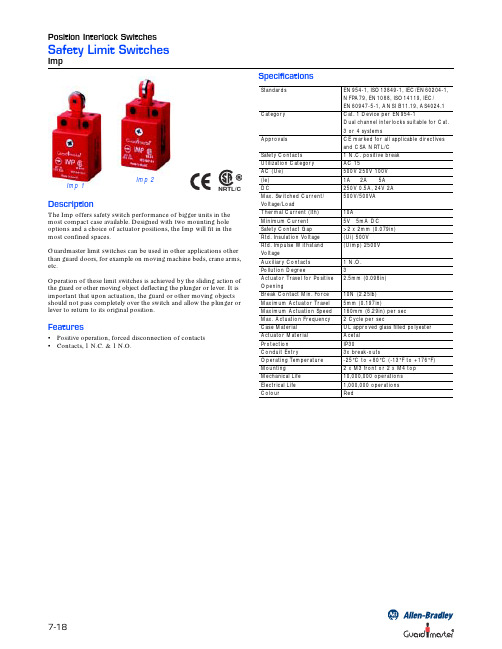
7-18Position Interlock SwitchesSafety Limit SwitchesImpDescriptionThe Imp offers safety switch performance of bigger units in the most compact case available. Designed with two mounting hole options and a choice of actuator positions, the Imp will fit in the most confined spaces.Guardmaster limit switches can be used in other applications other than guard doors, for example on moving machine beds, crane arms, etc.Operation of these limit switches is achieved by the sliding action of the guard or other moving object deflecting the plunger or lever. It is important that upon actuation, the guard or other moving objects should not pass completely over the switch and allow the plunger or lever to return to its original position.Features•Positive operation, forced disconnection of contacts •Contacts, 1 N.C. & 1 N.O.Imp 1Imp 2SpecificationsStandardsEN954-1, ISO13849-1, IEC/EN60204-1, NFPA79, EN1088, ISO14119, IEC/EN60947-5-1, ANSI B11.19, AS4024.1CategoryCat. 1 Device per EN954-1Dual channel interlocks suitable for Cat. 3 or 4 systemsApprovalsCE marked for all applicable directives and CSA NRTL/C Safety Contacts 1 N.C. positive break Utilization Category AC 15AC (Ue)500V 250V 100V (le)1A 2A 5A DC250V 0.5A, 24V 2A Max. Switched Current/Voltage/Load500V/500VA Thermal Current (lth)10AMinimum Current 5V 5mA DCSafety Contact Gap >2 x 2mm (0.079in)Rtd. Insulation Voltage (Ui) 500V Rtd. Impulse Withstand Voltage(Uimp) 2500V Auxiliary Contacts 1 N.O.Pollution Degree3Actuator Travel for Positive Opening2.5mm (0.098in)Break Contact Min. Force 10N (2.25lb)Maximum Actuator Travel 5mm (0.197in)Maximum Actuation Speed 160mm (6.29in) per sec Max. Actuation Frequency 2 Cycle per secCase Material UL approved glass filled polyester Actuator Material Acetal Protection IP30Conduit Entry3x break-outsOperating T emperature -25°C to +80°C (-13°F to +176°F)Mounting2 x M3 front or 2 x M4 top Mechanical Life 10,000,000 operations Electrical Life 1,000,000 operations ColourRedPosition Interlock Switches7-19Safety Limit SwitchesImpProduct SelectionDimensions—mm (inches)Connections。
1827185中文资料
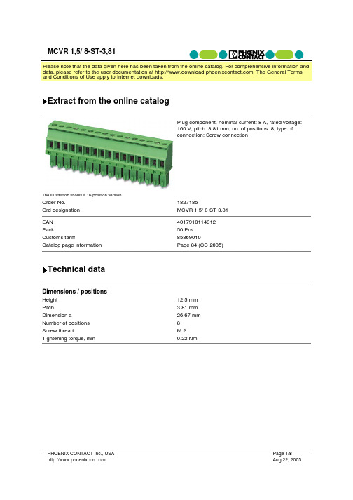
Extract from the online catalogThe illustration shows a 16-position version Plug component, nominal current: 8 A, rated voltage: 160 V, pitch: 3.81 mm, no. of positions: 8, type of connection: Screw connectionOrder No.Ord designation MCVR 1,5/ 8-ST-3,81 Catalog page information Page 84 (CC-2005) Technical dataTightening torque, min 0.22 NmTechnical dataInsulating material group IRated surge voltage (III/3) 2.5 kVRated surge voltage (III/2) 2.5 kVRated surge voltage (II/2) 2.5 kVRated voltage (III/2) 160 VRated voltage (II/2) 320 VConnection in acc. with standard EN-VDE8 ANominal current IN160 VNominal voltage UNNominal cross section 1.5 mm²Maximum load current 8 A (with 1.5 mm² conductor cross section) Insulating material PAInflammability class acc. to UL 94 V0Internal cylindrical gage A1Stripping length 7 mmConnection dataConductor cross section, rigid min. 0.14 mm²Conductor cross section, rigid max. 1.5 mm²Conductor cross section flexible min. 0.14 mm²Conductor cross section, flexible max. 1.5 mm²0.25 mm²Conductor cross section flexible, with ferrule withoutplastic sleeve min.Conductor cross section flexible, with ferrule without1.5 mm²plastic sleeve max.0.25 mm²Conductor cross section flexible, with ferrule with plasticsleeve min.0.5 mm²Conductor cross section flexible, with ferrule with plasticsleeve max.Conductor cross section AWG/kcmil min. 28Conductor cross section AWG/kcmil max 162 conductors with same cross section, solid min. 0.08 mm²2 conductors with same cross section, solid max. 0.5 mm²2 conductors with same cross section, flexible, min. 0.08 mm²2 conductors with same cross section, flexible max. 0.75 mm²0.25 mm²2 conductors with same cross section, flexible, ferruleswithout plastic sleeve min.0.34 mm²2 conductors with same cross section, flexible, ferruleswithout plastic sleeve, max.2 conductors with same cross section, flexible, TWIN0.5 mm²ferrules with plastic sleeve, min.2 conductors with identical cross section, flexible TWIN0.5 mm²ferrules with plastic sleeve, max.CertificatesCSA300 V Nominal voltage UNNominal current I8 ANAWG/kcmil 28-16 CULNominal voltage U300 VN8 A Nominal current INAWG/kcmil 30-14250 V Nominal voltage UNNominal current I8 ANAWG/kcmil 30-14 ULNominal voltage U300 VN8 A Nominal current INAWG/kcmil 30-14250 V Nominal voltage UN8 A Nominal current INAWG/kcmil 30-14Drawings Dimensioned drawingApproval logoAccessoriesItem Designation DescriptionMarking1051993B-STIFT Marker pen, for manual labeling of unprinted Zack strips, smear-proof and waterproof, line thickness 0.5 mm0804109SK 3,81/2,8:FORTL.ZAHLEN Marker card, printed horizontally, self-adhesive, 10-sectionmarker strip, 14 identical decades marked 1-10, 11-20 etc. up to91-(99)100, sufficient for 140 terminal blocks0805056SK 3,81/2,8:SO Marker card, special printing, self-adhesive, labeled acc. tocustomer requirements, 14 identical marker strips per card, max.25-position labeling per strip.0803883SK U/2,8 WH:UNBEDRUCKT Unprinted marker cards, DIN A4 format, pitch as desired, self-adhesive, with 50 stamped marker strips, 185 mm strip length,can be labeled with the CMS system or manually with the M-PENTools1205037SZS 0,4X2,5Screwdriver, bladed, matches all screw terminal blocks up to 1.5mm² connection cross section, blade: 0.4 x 2.5 mmAdditional productsItem Designation DescriptionGeneral1897869EMC 1,5/ 8-G-3,81Header, nominal current: 8 A, rated voltage: 160 V, pitch: 3.81mm, no. of positions: 8, mounting: press in1860702EMCV 1,5/ 8-G-3,81Header, nominal current: 8 A, rated voltage: 160 V, pitch: 3.81mm, no. of positions: 8, mounting: press in1857948IMC 1,5/ 8-ST-3,81Plug component, nominal current: 8 A, rated voltage: 160 V,pitch: 3.81 mm, no. of positions: 8, type of connection: Screwconnection1803332MC 1,5/ 8-G-3,81Header, nominal current: 8 A, rated voltage: 160 V, pitch: 3.81mm, no. of positions: 8, mounting: Soldering1908826MC 1,5/ 8-G-3,81 THT Header, nominal current: 8 A, rated voltage: 160 V, pitch: 3.81mm, no. of positions: 8, mounting: SMD / THT1830017MCD 1,5/ 8-G-3,81Header, nominal current: 7 A, rated voltage: 160 V, pitch: 3.81mm, no. of positions: 8, mounting: Soldering1843130MCD 1,5/ 8-G1-3,81Header, nominal current: 7 A, rated voltage: 160 V, pitch: 3.81mm, no. of positions: 8, mounting: Soldering1830460MCDV 1,5/ 8-G-3,81Header, nominal current: 7 A, rated voltage: 160 V, pitch: 3.81mm, no. of positions: 8, mounting: Soldering1847796MCDV 1,5/ 8-G1-3,81Header, nominal current: 7 A, rated voltage: 160 V, pitch: 3.81mm, no. of positions: 8, mounting: Soldering1861785MCO 1,5/ 8-GL-3,81Header, nominal current: 8 A, rated voltage: 125 V, pitch: 3.81mm, no. of positions: 8, mounting: Soldering1861701MCO 1,5/ 8-GR-3,81Header, nominal current: 8 A, rated voltage: 125 V, pitch: 3.81mm, no. of positions: 8, mounting: Soldering1803484MCV 1,5/ 8-G-3,81Header, nominal current: 8 A, rated voltage: 160 V, pitch: 3.81mm, no. of positions: 8, mounting: Soldering1908978MCV 1,5/ 8-G-3,81 THT Header, nominal current: 8 A, rated voltage: 160 V, pitch: 3.81mm, no. of positions: 8, mounting: SMD / THT1837492MCVDU 1,5/ 8-G-3,81Header, nominal current: 8 A, rated voltage: 160 V, pitch: 3.81mm, no. of positions: 8, mounting: Soldering1832798MCVK 1,5/ 8-G-3,81Header, nominal current: 8 A, rated voltage: 160 V, pitch: 3.81mm, no. of positions: 8, mounting: Mounting rail1827334SMC 1,5/ 8-G-3,81Header, nominal current: 8 A, rated voltage: 160 V, pitch: 3.81mm, no. of positions: 8, mounting: SolderingAddressPHOENIX CONTACT Inc., USA 586 Fulling Mill Road Middletown, PA 17057USAPhone (800) 888-7388Fax (717) 944-1625 Phoenix ContactTechnical modifications reserved;。
LV244A中文资料

PACKAGING INFORMATIONOrderable Device Status(1)PackageType PackageDrawingPins PackageQtyEco Plan(2)Lead/Ball Finish MSL Peak Temp(3)SN74LV244ADBLE OBSOLETE SSOP DB20TBD Call TI Call TISN74LV244ADBR ACTIVE SSOP DB202000Green(RoHS&no Sb/Br)CU NIPDAU Level-1-260C-UNLIMSN74LV244ADBRE4ACTIVE SSOP DB202000Green(RoHS&no Sb/Br)CU NIPDAU Level-1-260C-UNLIMSN74LV244ADGVR ACTIVE TVSOP DGV202000Green(RoHS&no Sb/Br)CU NIPDAU Level-1-260C-UNLIMSN74LV244ADGVRE4ACTIVE TVSOP DGV202000Green(RoHS&no Sb/Br)CU NIPDAU Level-1-260C-UNLIMSN74LV244ADW ACTIVE SOIC DW2025Green(RoHS&no Sb/Br)CU NIPDAU Level-1-260C-UNLIMSN74LV244ADWE4ACTIVE SOIC DW2025Green(RoHS&no Sb/Br)CU NIPDAU Level-1-260C-UNLIMSN74LV244ADWR ACTIVE SOIC DW202000Green(RoHS&no Sb/Br)CU NIPDAU Level-1-260C-UNLIMSN74LV244ANSR ACTIVE SO NS202000Green(RoHS&no Sb/Br)CU NIPDAU Level-1-260C-UNLIMSN74LV244ANSRE4ACTIVE SO NS202000Green(RoHS&no Sb/Br)CU NIPDAU Level-1-260C-UNLIMSN74LV244ANSRG4ACTIVE SO NS202000Green(RoHS&no Sb/Br)CU NIPDAU Level-1-260C-UNLIMSN74LV244APW ACTIVE TSSOP PW2070Green(RoHS&no Sb/Br)CU NIPDAU Level-1-260C-UNLIMSN74LV244APWE4ACTIVE TSSOP PW2070Green(RoHS&no Sb/Br)CU NIPDAU Level-1-260C-UNLIMSN74LV244APWG4ACTIVE TSSOP PW2070Green(RoHS&no Sb/Br)CU NIPDAU Level-1-260C-UNLIM SN74LV244APWLE OBSOLETE TSSOP PW20TBD Call TI Call TISN74LV244APWR ACTIVE TSSOP PW202000Green(RoHS&no Sb/Br)CU NIPDAU Level-1-260C-UNLIMSN74LV244APWRE4ACTIVE TSSOP PW202000Green(RoHS&no Sb/Br)CU NIPDAU Level-1-260C-UNLIMSN74LV244APWRG4ACTIVE TSSOP PW202000Green(RoHS&no Sb/Br)CU NIPDAU Level-1-260C-UNLIMSN74LV244APWT ACTIVE TSSOP PW20250Green(RoHS&no Sb/Br)CU NIPDAU Level-1-260C-UNLIMSN74LV244APWTE4ACTIVE TSSOP PW20250Green(RoHS&no Sb/Br)CU NIPDAU Level-1-260C-UNLIMSN74LV244ARGYR ACTIVE QFN RGY201000Green(RoHS&no Sb/Br)CU NIPDAU Level-2-260C-1YEAR SN74LV244ARGYRG4ACTIVE QFN RGY20TBD Call TI Call TI(1)The marketing status values are defined as follows:ACTIVE:Product device recommended for new designs.LIFEBUY:TI has announced that the device will be discontinued,and a lifetime-buy period is in effect.NRND:Not recommended for new designs.Device is in production to support existing customers,but TI does not recommend using this part in a new design.PREVIEW:Device has been announced but is not in production.Samples may or may not be available.OBSOLETE:TI has discontinued the production of the device.(2)Eco Plan-The planned eco-friendly classification:Pb-Free(RoHS),Pb-Free(RoHS Exempt),or Green(RoHS&no Sb/Br)-please check /productcontent for the latest availability information and additional product content details.TBD:The Pb-Free/Green conversion plan has not been defined.Pb-Free(RoHS):TI's terms"Lead-Free"or"Pb-Free"mean semiconductor products that are compatible with the current RoHS requirements for all6substances,including the requirement that lead not exceed0.1%by weight in homogeneous materials.Where designed to be soldered at high temperatures,TI Pb-Free products are suitable for use in specified lead-free processes.Pb-Free(RoHS Exempt):This component has a RoHS exemption for either1)lead-based flip-chip solder bumps used between the die and package,or2)lead-based die adhesive used between the die and leadframe.The component is otherwise considered Pb-Free(RoHS compatible)as defined above.Green(RoHS&no Sb/Br):TI defines"Green"to mean Pb-Free(RoHS compatible),and free of Bromine(Br)and Antimony(Sb)based flame retardants(Br or Sb do not exceed0.1%by weight in homogeneous material)(3)MSL,Peak Temp.--The Moisture Sensitivity Level rating according to the JEDEC industry standard classifications,and peak solder temperature.Important Information and Disclaimer:The information provided on this page represents TI's knowledge and belief as of the date that it is provided.TI bases its knowledge and belief on information provided by third parties,and makes no representation or warranty as to the accuracy of such information.Efforts are underway to better integrate information from third parties.TI has taken and continues to take reasonable steps to provide representative and accurate information but may not have conducted destructive testing or chemical analysis on incoming materials and chemicals.TI and TI suppliers consider certain information to be proprietary,and thus CAS numbers and other limited information may not be available for release.In no event shall TI's liability arising out of such information exceed the total purchase price of the TI part(s)at issue in this document sold by TI to Customer on an annual basis.元器件交易网IMPORTANT NOTICETexas Instruments Incorporated and its subsidiaries (TI) reserve the right to make corrections, modifications,enhancements, improvements, and other changes to its products and services at any time and todiscontinue any product or service without notice. Customers should obtain the latest relevant informationbefore placing orders and should verify that such information is current and complete. All products are soldsubject to TI’s terms and conditions of sale supplied at the time of order acknowledgment.TI warrants performance of its hardware products to the specifications applicable at the time of sale inaccordance with TI’s standard warranty. Testing and other quality control techniques are used to the extentTI deems necessary to support this warranty. Except where mandated by government requirements, testingof all parameters of each product is not necessarily performed.TI assumes no liability for applications assistance or customer product design. Customers are responsiblefor their products and applications using TI components. To minimize the risks associated with customerproducts and applications, customers should provide adequate design and operating safeguards.TI does not warrant or represent that any license, either express or implied, is granted under any TI patentright, copyright, mask work right, or other TI intellectual property right relating to any combination, machine,or process in which TI products or services are used. Information published by TI regarding third-partyproducts or services does not constitute a license from TI to use such products or services or a warranty orendorsement thereof. Use of such information may require a license from a third party under the patents orother intellectual property of the third party, or a license from TI under the patents or other intellectualproperty of TI.Reproduction of information in TI data books or data sheets is permissible only if reproduction is withoutalteration and is accompanied by all associated warranties, conditions, limitations, and notices.Reproduction of this information with alteration is an unfair and deceptive business practice. TI is notresponsible or liable for such altered documentation.Resale of TI products or services with statements different from or beyond the parameters stated by TI forthat product or service voids all express and any implied warranties for the associated TI product or serviceand is an unfair and deceptive business practice. TI is not responsible or liable for any such statements.Following are URLs where you can obtain information on other Texas Instruments products and applicationsolutions:Products ApplicationsAmplifiers Audio /audioData Converters Automotive /automotive/broadband DSP BroadbandControl /digitalcontrolDigitalInterface Logic Military /military Power Mgmt Optical Networking /opticalnetworkSecurity /securityMicrocontrollers Low Power Wireless /lpw Telephony /telephonyVideo & Imaging /videoWireless/wirelessMailing Address: Texas InstrumentsPost Office Box 655303 Dallas, Texas 75265Copyright © 2007, Texas Instruments Incorporated。
ADR443A中文资料
Ultralow Noise, LDO XFET® VoltageReferences with Current Sink and SourceADR440/ADR441/ADR443/ADR444/ADR445 Rev. AInformation furnished by Analog Devices is believed to be accurate and reliable. However, noresponsibility is assumed by Analog Devices for its use, nor for any infringements of patents or other rights of third parties that may result from its use. Specifications subject to change without notice. No license is granted by implication or otherwise under any patent or patent rights of Analog Devices. T rademarks and registered trademarks are the property of their respective owners. One Technology Way, P.O. Box 9106, Norwood, M A 02062-9106, U.S.A. Tel: 781.329.4700 Fax: 781.461.3113 ©2006 Analog Devices, Inc. All rights reserved.FEATURESUltralow noise (0.1 Hz to 10 Hz)ADR440: 1 μV p-pADR441: 1.2 μV p-pADR443: 1.4 μV p-pADR444: 1.8 μV p-pADR445: 2.25 μV p-pSuperb temperature coefficientA Grade: 10 ppm/°CB Grade: 3 ppm/°CLow dropout operation: 500 mVInput range: (V OUT + 500 mV) to 18 VHigh output source and sink current: +10 mA and −5 mA Wide temperature range: −40°C to +125°C APPLICATIONSPrecision data acquisition systemsHigh resolution data convertersBattery-powered instrumentationsPortable medical instrumentsIndustrial process control systemsPrecision instrumentsOptical control circuitsPIN CONFIGURATIONS NOTES1. NC = NO CONNECT2. TP = TEST PIN (DO NOT CONNECT)TPV INNCGNDTPNCV OUTTRIM5428-1 Figure 1. 8-Lead SOIC_N (R-Suffix)5428-2 TPV INNCGNDTPNCV OUTTRIMNOTES1. NC = NO CONNECT2. TP = TEST PIN (DO NOT CONNECT) Figure 2. 8-Lead MSOP (RM-Suffix)GENERAL DESCRIPTIONThe ADR44x series is a family of XFET voltage references featuring ultralow noise, high accuracy, and low temperature drift performance. Using Analog Devices, Inc., patented temperature drift curvature correction and XFET (eXtra implanted junction FET) technology, voltage change vs. temperature nonlinearity in the ADR44x is greatly minimized. The XFET references offer better noise performance than buried Zener references, and XFET references operate offlow supply voltage headroom (0.5 V). This combination of features makes the ADR44x family ideally suited for precision signal conversion applications in high-end data acquisition systems, optical networks, and medical applications.The ADR44x family has the capability to source up to 10 mA of output current and sink up to 5 mA. It also comes with a trim terminal to adjust the output voltage over a 0.5% range without compromising performance. Offered in two electrical grades, the ADR44x family is avail-able in 8-lead MSOP and narrow SOIC packages. All versions are specified over the extended industrial temperature range of −40°C to +125°C.Table 1. Selection GuideModelOutputVoltage(V)InitialAccuracy, ±(mV)TemperatureCoefficient(ppm/°C)ADR440A 2.048 3 10ADR440B 2.048 1 3ADR441A 2.500 3 10ADR441B 2.500 1 3ADR443A 3.000 4 10ADR443B 3.000 1.2 3ADR444A 4.096 5 10ADR444B 4.096 1.6 3ADR445A 5.000 6 10ADR445B 5.000 2 3ADR440/ADR441/ADR443/ADR444/ADR445Rev. A | Page 2 of 20TABLE OF CONTENTSFeatures..............................................................................................1 Applications.......................................................................................1 Pin Configurations...........................................................................1 General Description.........................................................................1 Revision History...............................................................................2 Specifications.....................................................................................3 ADR440 Electrical Characteristics.............................................3 ADR441 Electrical Characteristics.............................................4 ADR443 Electrical Characteristics.............................................5 ADR444 Electrical Characteristics.............................................6 ADR445 Electrical Characteristics.............................................7 Absolute Maximum Ratings............................................................8 Thermal Resistance......................................................................8 ESD Caution..................................................................................8 Typical Performance Characteristics.............................................9 Theory of Operation......................................................................14 Power Dissipation Considerations...........................................14 Basic Voltage Reference Connections.....................................14 Noise Performance.....................................................................14 Turn-On Time............................................................................14 Applications.....................................................................................15 Output Adjustment....................................................................15 Bipolar Outputs..........................................................................15 Negative Reference.....................................................................15 Programmable Voltage Source.................................................16 Programmable Current Source................................................16 High Voltage Floating Current Source....................................16 Precision Output Regulator (Boosted Reference)..................17 Outline Dimensions.......................................................................18 Ordering Guide.. (19)REVISION HISTORY9/06—Rev. 0 to Rev. AUpdated Format..................................................................Universal Changes to Features..........................................................................1 Changes to Pin Configurations.......................................................1 Changes to the Specifications Section...........................................3 Changes to Figure 4 and Figure 5...................................................9 Inserted Figure 6 and Figure 7........................................................9 Changes to Figure 15......................................................................11 Changes to the Power Dissipation Considerations Section......14 Changes to Figure 35 and Figure 36.............................................15 Changes to Figure 38 and Table 9.................................................16 Updated Outline Dimensions.......................................................18 Changes to Ordering Guide..........................................................19 10/05—Revision 0: Initial VersionADR440/ADR441/ADR443/ADR444/ADR445Rev. A | Page 3 of 20SPECIFICATIONSADR440 ELECTRICAL CHARACTERISTICSV IN = 3 V to 18 V , T A = 25°C, C IN = C OUT = 0.1 μF, unless otherwise noted. Table 2.Parameter Symbol Conditions M in Typ M ax Unit OUTPUT VOL TAGE V O A Grade 2.045 2.048 2.051 V B Grade 2.047 2.048 2.049 V INITIAL ACCURACY V OERR A Grade 3 mV 0.15 % B Grade 1 mV 0.05 % TEMPERATURE DRIFT TCV O A Grade −40°C < T A < +125°C 2 10 ppm/°C B Grade −40°C < T A < +125°C 1 3 ppm/°C LINE REGULATION ΔV O /ΔV IN −40°C < T A < +125°C −20 +10 +20 ppm/V LOAD REGULATION ΔV O /ΔI LOAD I LOAD = 0 mA to 10 mA, V IN = 3.5 V,−40°C < T A < +125°C−50 +50 ppm/mA ΔV O /ΔI LOAD I LOAD = 0 mA to −5 mA, V IN = 3.5 V,−40°C < T A < +125°C−50 +50 ppm/mA QUIESCENT CURRENT I IN No load, −40°C < T A < +125°C 3 3.75 mA VOLTAGE NOISE e N p-p 0.1 Hz to 10 Hz 1 μV p-p VOLTAGE NOISE DENSITY e N 1 kHz 45 nV/√Hz TURN-ON SETTLING TIME t R 10 μs LONG-TERM STABILITY 1V O 1000 hours 50 ppm OUTPUT VOL TAGE HYSTERESIS V O_HYS 70 ppm RIPPLE REJECTION RATIO RRR f IN = 10 kHz −75 dB SHORT CIRCUIT TO GND I SC 27 mA SUPPLY VOL TAGE OPERATING RANGE V IN 3 18 V SUPPLY VOL TAGE HEADROOM V IN − V O 500 mV1The long-term stability specification is noncumulative. The drift in the subsequent 1000-hour period is significantly lower than in the first 1000-hour period.ADR440/ADR441/ADR443/ADR444/ADR445Rev. A | Page 4 of 20ADR441 ELECTRICAL CHARACTERISTICSV IN = 3 V to 18 V , T A = 25°C, C IN = C OUT = 0.1 μF, unless otherwise noted. Table 3.Parameter Symbol Conditions M in Typ Max Unit OUTPUT VOL TAGE V O A Grade 2.497 2.500 2.503 V B Grade 2.499 2.500 2.501 V INITIAL ACCURACY V OERR A Grade3 mV 0.12 % B Grade 1 mV 0.04 % TEMPERATURE DRIFT TCV O A Grade −40°C < T A < +125°C 2 10 ppm/°C B Grade −40°C < T A < +125°C 1 3 ppm/°C LINE REGULATION ΔV O /ΔV IN −40°C < T A < +125°C 10 20 ppm/V LOAD REGULATION ΔV O /ΔI LOAD I LOAD = 0 mA to 10 mA, V IN = 4 V,−40°C < T A < +125°C−50 +50 ppm/mA ΔV O /ΔI LOAD I LOAD = 0 mA to −5 mA, V IN = 4 V,−40°C < T A < +125°C−50 +50 ppm/mA QUIESCENT CURRENT I IN No load, −40°C < T A < +125°C 3 3.75 mA VOLTAGE NOISE e N p-p 0.1 Hz to 10 Hz 1.2 μV p-p VOLTAGE NOISE DENSITY e N 1 kHz 48 nV/√Hz TURN-ON SETTLING TIME t R 10 μsLONG-TERM STABILITY 1V O 1000 hours 50 ppm OUTPUT VOL TAGE HYSTERESIS V O_HYS 70 ppm RIPPLE REJECTION RATIO RRR f IN = 10 kHz −75 dB SHORT CIRCUIT TO GND I SC 27 mA SUPPL Y VOL TAGE OPERATING RANGE V IN 3 18 V SUPPLY VOL TAGE HEADROOM V IN − V O 500 mV1The long-term stability specification is noncumulative. The drift in subsequent 1000-hour period is significantly lower than in the first 1000-hour period.ADR440/ADR441/ADR443/ADR444/ADR445Rev. A | Page 5 of 20ADR443 ELECTRICAL CHARACTERISTICSV IN = 3.5 V to 18 V , T A = 25°C, C IN = C OUT = 0.1 μF, unless otherwise noted. Table 4.Parameter Symbol Conditions M in Typ M ax Unit OUTPUT VOL TAGE V O A Grade 2.996 3.000 3.004 V B Grade 2.9988 3.000 3.0012 V INITIAL ACCURACY V OERR A Grade4 mV 0.13 % B Grade 1.2 mV 0.04 % TEMPERATURE DRIFT TCV O A Grade −40°C < T A < +125°C 2 10 ppm/°C B Grade −40°C < T A < +125°C 1 3 ppm/°C LINE REGULATION ΔV O /ΔV IN −40°C < T A < +125°C 10 20 ppm/V LOAD REGULATION ΔV O /ΔI LOAD I LOAD = 0 mA to 10 mA, V IN =5 V,−40°C < T A < +125°C−50 +50 ppm/mA ΔV O /ΔI LOAD I LOAD = 0 mA to −5 mA, V IN = 5 V,−40°C < T A < +125°C−50 +50 ppm/mA QUIESCENT CURRENT I IN No load, −40°C < T A < +125°C 3 3.75 mA VOLTAGE NOISE e N p-p 0.1 Hz to 10 Hz 1.4 μV p-p VOLTAGE NOISE DENSITY e N 1 kHz 57.6 nV/√Hz TURN-ON SETTLING TIME t R 10 μs LONG-TERM STABILITY 1V O 1000 hours 50 ppm OUTPUT VOL TAGE HYSTERESIS V O_HYS 70 ppm RIPPLE REJECTION RATIO RRR f IN = 10 kHz −75 dB SHORT CIRCUIT TO GND I SC 27 mA SUPPLY VOL TAGE OPERATING RANGE V IN 3.5 18 V SUPPLY VOL TAGE HEADROOM V IN − V O 500 mV1The long-term stability specification is noncumulative. The drift in the subsequent 1000-hour period is significantly lower than in the first 1000-hour period.ADR440/ADR441/ADR443/ADR444/ADR445Rev. A | Page 6 of 20ADR444 ELECTRICAL CHARACTERISTICSV IN = 4.6 V to 18 V , T A = 25°C, C IN = C OUT = 0.1 μF, unless otherwise noted. Table 5.Parameter Symbol Conditions M in Typ Max Unit OUTPUT VOL TAGE V O A Grade 4.091 4.096 4.101 V B Grade 4.0944 4.096 4.0976 V INITIAL ACCURACY V OERR A Grade5 mV 0.13 % B Grade 1.6 mV 0.04 % TEMPERATURE DRIFT TCV O A Grade −40°C < T A < +125°C 2 10 ppm/°C B Grade −40°C < T A < +125°C 1 3 ppm/°C LINE REGULATION ΔV O /ΔV IN −40°C < T A < +125°C 10 20 ppm/V LOAD REGULATION ΔV O /ΔI LOAD I LOAD = 0 mA to 10 mA, V IN = 5.5 V,−40°C < T A < +125°C−50 +50 ppm/mA ΔV O /ΔI LOAD I LOAD = 0 mA to −5 mA, V IN = 5.5 V,−40°C < T A < +125°C−50 +50 ppm/mA QUIESCENT CURRENT I IN No load, −40°C < T A < +125°C 3 3.75 mA VOLTAGE NOISE e N p-p 0.1 Hz to 10 Hz 1.8 μV p-p VOLTAGE NOISE DENSITY e N 1 kHz 78.6 nV/√Hz TURN-ON SETTLING TIME t R 10 μsLONG-TERM STABILITY 1V O 1000 hours 50 ppm OUTPUT VOL TAGE HYSTERESIS V O_HYS 70 ppm RIPPLE REJECTION RATIO RRR f IN = 10 kHz −75 dB SHORT CIRCUIT TO GND I SC 27 mA SUPPLY VOL TAGE OPERATING RANGE V IN 4.6 18 V SUPPLY VOL TAGE HEADROOM V IN − V O 500 mV1The long-term stability specification is noncumulative. The drift in the subsequent 1000-hour period is significantly lower than in the first 1000-hour period.ADR440/ADR441/ADR443/ADR444/ADR445Rev. A | Page 7 of 20ADR445 ELECTRICAL CHARACTERISTICSV IN = 5.5 V to 18 V , T A = 25°C, C IN = C OUT = 0.1 μF, unless otherwise noted. Table 6.Parameter Symbol Conditions M in Typ Max Unit OUTPUT VOL TAGE V O A Grade 4.994 5.000 5.006 V B Grade 4.998 5.000 5.002 V INITIAL ACCURACY V OERR A Grade 6 mV 0.12 % B Grade 2 mV 0.04 % TEMPERATURE DRIFT TCV O A Grade −40°C < T A < +125°C 2 10 ppm/°C B Grade −40°C < T A < +125°C 1 3 ppm/°C LINE REGULATION ΔV O /ΔV IN −40°C < T A < +125°C 10 20 ppm/V LOAD REGULATION ΔV O /ΔI LOAD I LOAD = 0 mA to 10 mA, V IN = 6.5 V,−40°C < T A < +125°C−50 +50 ppm/mA ΔV O /ΔI LOAD I LOAD = 0 mA to −5 mA, V IN = 6.5 V,−40°C < T A < +125°C−50 +50 ppm/mA QUIESCENT CURRENT I IN No load, −40°C < T A < +125°C 3 3.75 mA VOLTAGE NOISE e N p-p 0.1 Hz to 10 Hz 2.25 μV p-p VOLTAGE NOISE DENSITY e N 1 kHz 90 nV/√Hz TURN-ON SETTLING TIME t R 10 μsLONG-TERM STABILITY 1V O 1000 hours 50 ppm OUTPUT VOL TAGE HYSTERESIS V O_HYS 70 ppm RIPPLE REJECTION RATIO RRR f IN = 10 kHz –75 dB SHORT CIRCUIT TO GND I SC 27 mA SUPPLY VOL TAGE OPERATING RANGE V IN 5.5 18 V SUPPLY VOL TAGE HEADROOM V IN − V O 500 mV1The long-term stability specification is noncumulative. The drift in the subsequent 1000-hour period is significantly lower than in the first 1000-hour period.ADR440/ADR441/ADR443/ADR444/ADR445Rev. A | Page 8 of 20ABSOLUTE MAXIMUM RATINGST A = 25°C, unless otherwise noted. Table 7.Parameter RatingSupply Voltage 20 VOutput Short-Circuit Duration to GND IndefiniteStorage Temperature Range −65°C to +125°C Operating Temperature Range −40°C to +125°C Junction Temperature Range −65°C to +150°CLead Temperature, Soldering (60 sec) 300°CStresses above those listed under Absolute Maximum Ratings may cause permanent damage to the device. This is a stress rating only; functional operation of the device at these or any other conditions above those indicated in the operationalsection of this specification is not implied. Exposure to absolute maximum rating conditions for extended periods may affect device reliability. THERMAL RESISTANCEθJA is specified for the worst-case conditions, that is, a device soldered in a circuit board for surface-mount packages.Table 8. Thermal Resistance Package Type θJA θJC Unit 8-Lead SOIC_N (R-Suffix) 130 43 °C/W8-Lead MSOP (RM-Suffix) 190°C/WESD CAUTIONADR440/ADR441/ADR443/ADR444/ADR445Rev. A | Page 9 of 20TYPICAL PERFORMANCE CHARACTERISTICSV IN = 7 V , T A = 25°C, C IN = C OUT = 0.1 μF, unless otherwise noted.TEMPERATURE (°C)O U T P U T V O L T A G E (V )2.50202.50152.50052.50102.50002.49952.4990–405–10–2550352011095806512505428-003Figure 3. ADR441 Output Voltage vs. TemperatureTEMPERATURE (°C)O U T P U T V O L T A G E (V )3.00203.00153.00003.00053.00102.99952.99852.99902.9980Figure 4. ADR443 Output Voltage vs. TemperatureTEMPERATURE (°C)O U T P U T V O L T A G E (V )4.09804.09754.09604.09654.09704.09554.09454.09504.0940Figure 5. ADR444 Output Voltage vs. Temperature 2.0512.0502.0492.0482.0472.0462.045–40–20020100806040120TEMPERATURE (°C)O U T P U T V O L T A G E (V )05428-042Figure 6. ADR440 Output Voltage vs. Temperature5.0065.0045.0025.0004.9984.9964.994–40–20020100806040120TEMPERATURE (°C)O U T P U T V O L T A G E (V )05428-043Figure 7. ADR445 Output Voltage vs. TemperatureINPUT VOLTAGE (V)S U P P L Y C U R R E NT (m A )4.03.53.02.52.0Figure 8. ADR441 Supply Current vs. Input VoltageADR440/ADR441/ADR443/ADR444/ADR445Rev. A | Page 10 of 20TEMPERATURE (°C)S U P P L Y C U R R E N T (m A )4.03.53.02.52.0–405–10–2550352011095806512505428-007Figure 9. ADR441 Supply Current vs. TemperatureINPUT VOLTAGE (V)S U P P L Y C U R R E N T (m A )05428-008Figure 10. ADR445 Supply Current vs. Input VoltageTEMPERATURE (°C)Q U I E S C E N T C U R R E N T (m A )3.253.153.052.952.852.75–405–10–2550352011095806512505428-009Figure 11. ADR445 Quiescent Current vs. Temperature TEMPERATURE (°C)L I N E R E G U L A T I O N (p p m /V )1086240–405–10–2550352011095806512505428-010Figure 12. ADR441 Line Regulation vs. TemperatureTEMPERATURE (°C)L O A D R E G U L A T I O N (p p m /m A )60555040354530Figure 13. ADR441 Load Regulation vs. TemperatureTEMPERATURE (°C)L I N E R E G U L A T I O I N (p p m /V )76541230–405–10–2550352011095806512505428-012Figure 14. ADR445 Line Regulation vs. TemperatureADR440/ADR441/ADR443/ADR444/ADR445TEMPERATURE (°C)L O A D R E G U L A T I O N (p p m /m A )50403020–30–40–20–10010–5005428-013Figure 15. ADR445 Load Regulation vs. TemperatureLOAD CURRENT (mA)D I F FE R E N T I A L V O L T A G E (V )0.70.60.50.30.20.10.4005428-014Figure 16. ADR441 Minimum Input/Output Differential Voltage vs. Load CurrentTEMPERATURE (°C)M I N I M U MH E A D R O O M (V )0.50.40.30.20.1005428-015Figure 17. ADR441 Minimum Headroom vs. TemperatureLOAD CURRENT (mA)D I F FE R E N T I AL V O L T A G E (V )1.00.90.80.70.60.50.30.20.10.40Figure 18. ADR445 Minimum Input/Output Differential Voltage vs. Load CurrentTEMPERATURE (°C)M I N I M UM H E A D R O O M (V )0.50.40.30.20.1Figure 19. ADR445 Minimum Headroom vs. Temperature05428-018V OUT = 1V/DIVV IN = 5V/DIVC IN , C OUT = 0.1µFTIME = 10µs/DIVFigure 20. ADR441 Turn-On ResponseADR440/ADR441/ADR443/ADR444/ADR44505428-019V OUT = 1V/DIVV IN = 5V/DIVC IN , C OUT = 0.1µFTIME = 200µs/DIVFigure 21. ADR441 Turn-Off Response05428-020V OUT = 1V/DIVV IN = 5V/DIVC IN = 0.1µF C OUT = 10µFTIME = 200µs/DIVFigure 22. ADR441 Turn-On Response05428-0212V/DIV4V2mV/DIVC IN = 0.1µF C OUT = 10µFTIME = 100µs/DIVFigure 23. ADR441 Line Transient Response05428-022LOAD OFFLOAD ON5mV/DIVC IN , C OUT = 0.1µF TIME = 200µs/DIVFigure 24. ADR441 Load Transient Response05428-023LOAD OFFLOAD ON5mV/DIVC IN = 0.1µF C OUT = 10µF TIME = 200µs/DIVFigure 25. ADR441 Load Transient Response05428-024CH1 p-p 1.18µV1µV/DIVTIME = 1s/DIVFigure 26. ADR441 0.1 Hz to 10.0 Hz Voltage NoiseADR440/ADR441/ADR443/ADR444/ADR44505428-025CH1 p-p 49µVFigure 27. ADR441 10 Hz to 10 kHz Voltage Noise05428-026CH1 p-p 2.24µVFigure 28. ADR445 0.1 Hz to 10.0 Hz Voltage Noise05428-027CH1 p-p 66µVFigure 29. ADR445 10 Hz to 10 kHz Voltage Noise DEVIATION (PPM)N U M B E R O F P A R T S1601412108642–130–150–11–90–70–50–1–3135711913015Figure 30. ADR441 Typical Output Voltage HysteresisFREQUENCY (Hz)O U T P U T I M P E D A N C E (Ω)10987564321Figure 31. Output Impedance vs. FrequencyFREQUENCY (Hz)R I P P L E R E J E C T I O N R A T I O (d B )100k 1M10k 1k 10005428-030–100–20–30–40–50–60–70–80–90–100Figure 32. Ripple Rejection Ratio vs. FrequencyADR440/ADR441/ADR443/ADR444/ADR445THEORY OF OPERATIONThe ADR44x series of references uses a new reference generation technique known as XFET (eXtra implanted junction FET). This technique yields a reference with low dropout, good thermal hysteresis, and exceptionally low noise. The core of the XFET reference consists of two junction field-effect transistors (JFETs), one of which has an extra channel implant to raise its pinch-off voltage. By running the two JFETs at the same drain current, the difference in pinch-off voltage can be amplified and used to form a highly stable voltage reference.The intrinsic reference voltage is around 0.5 V with a negative temperature coefficient of about –120 ppm/°C. This slope isessentially constant to the dielectric constant of silicon, and it can be closely compensated for by adding a correction term generated in the same fashion as the proportional-to-temperature (PTAT) term used to compensate band gap references. The advantage of an XFET reference is its correction term, which is approx-imately 20 times lower and requires less correction than that of a band gap reference. Because most of the noise of a band gap reference comes from the temperature compensation circuitry, the XFET results in much lower noise.Figure 33 shows the basic topology of the ADR44x series. The temperature correction term is provided by a current source with a value designed to be proportional to absolute temperature. The general equation is()PTAT P OUT I R1V G V ×−=Δ (1) where:G is the gain of the reciprocal of the divider ratio.ΔV P is the difference in pinch-off voltage between the two JFETs. I PTAT is the positive temperature coefficient correction current. ADR44x devices are created by on-chip adjustment of R2 and R3 to achieve the different voltage option at the reference output.I PTATOUT P PTAT INOUT05428-033Figure 33. Simplified Schematic DevicePOWER DISSIPATION CONSIDERATIONSThe ADR44x family of references is guaranteed to deliver load currents to 10 mA with an input voltage that ranges from 3 V to 18 V . When these devices are used in applications at higher currents, users should use the following equation to account for the temperature effects of increases in power dissipation:A JA D J T P T +θ×= (2) where:T J and T A are the junction and ambient temperatures, respectively.P D is the device power dissipation.θJA is the device package thermal resistance.BASIC VOLTAGE REFERENCE CONNECTIONSThe ADR44x family requires a 0.1 μF capacitor on the input and the output for stability. While not required for operation, a 10 μF capacitor at the input can help with line voltage transient performance.NOTES1. NC = NO CONNECT2. TP = TEST PIN (DO NOT CONNECT)05428-034VFigure 34. Basic Voltage Reference ConfigurationNOISE PERFORMANCEThe noise generated by the ADR44x family of references is typically less than 1.4 μV p-p over the 0.1 Hz to 10.0 Hz band for ADR440, ADR441, and ADR443. Figure 26 shows the 0.1 Hz to 10 Hz noise of the ADR441, which is only 1.2 μV p-p. The noise measurement is made with a band-pass filter made of a 2pole high-pass filter with a corner frequency at 0.1 Hz and a 2pole low-pass filter with a corner frequency at 10.0 Hz.TURN-ON TIMEUpon application of power (cold start), the time required for the output voltage to reach its final value within a specified error band is defined as the turn-on settling time . Two compo-nents normally associated with this are the time for the active circuits to settle and the time for the thermal gradients on the chip to stabilize. Figure 20 and Figure 21 show the turn-on and turn-off settling times for the ADR441.ADR440/ADR441/ADR443/ADR444/ADR445APPLICATIONSOUTPUT ADJUSTMENTThe ADR44x family features a TRIM pin that allows the user to adjust the output voltage of the part over a limited range. This allows errors from the reference and overall system errors to be trimmed out by connecting a potentiometer between the output and the ground, with the wiper connected to the TRIM pin. Figure 35 shows the optimal trim configuration. R1 allows fine adjustment of the output and is not always required. R P should be sufficiently large so that the maximum output current from the ADR44x is not exceeded.V O = ±0.5%05428-035Figure 35. ADR44x Trim FunctionUsing the trim function has a negligible effect on the temperature performance of the ADR44x. However, all resistors need to be low temperature coefficient resistors, or errors can occur.BIPOLAR OUTPUTSBy connecting the output of the ADR44x to the invertingterminal of an operational amplifier, it is possible to obtain both positive and negative reference voltages. Care must be taken when choosing Resistor R1 and Resistor R2 (see Figure 36). They must be matched as closely as possible to ensure minimal differences between the negative and positive outputs. In addition, care must be taken to ensure performance over temperature. Use low temperature coefficient resistors if the circuit is used over temperature; otherwise, differences exist between the two outputs.–5V05428-036Figure 36. ADR44x Bipolar OutputsNEGATIVE REFERENCEFigure 37 shows how to connect the ADR44x and a standard operational amplifier, such as the OP1177, to provide negative voltage. This configuration provides two main advantages. First, it only requires two devices; therefore, it does not require excessive board space. Second, and more importantly, it does not require any external resistors. This means the performance of this circuit does not rely on choosing low temperature coefficient resistors to ensure accuracy.REF05428-037Figure 37. ADR44x Negative ReferenceV OUT is at virtual ground, and the negative reference is taken directly from the output of the operational amplifier. If the negative supply voltage is close to the reference output, the operational amplifier must be dual supply and have low offset and rail-to-rail capability.ADR440/ADR441/ADR443/ADR444/ADR445PROGRAMMABLE VOLTAGE SOURCETo obtain different voltages than those offered by the ADR44x, some extra components are needed. In Figure 38, two potentiometers are used to set the desired voltage, while the buffering amplifier provides current drive. The potentiometer connected between V OUT and GND, with its wiper connected to the noninverting input of the operational amplifier, takes care of coarse trim. The second potentiometer, with its wiperconnected to the trim terminal of the ADR44x, is used for fine adjustment. Resolution depends on the end-to-end resistance value and the resolution of the selected potentiometer.REF05428-038Figure 38. Programmable Voltage SourceFor a completely programmable solution, replace the two potentiometers in Figure 38 with one Analog Devices dual digital potentiometer, offered with either an SPI® or an I 2C® interface. These interfaces set the position of the wiper on both potentiometers and allow the output voltage to be set. Table 9 lists compatible Analog Devices digital potentiometers. Table 9. Digital Potentiometer PartsPart No. No. ofChannels No. ofPositions ITF R (kΩ)V DD 1AD5251 2.00 64.00 I 2C 1, 10, 50, 100 5.5AD5207 2.00 256.00 SPI 10, 50, 1005.5 AD5242 2.00 256.00 I 2C 10, 100, 1M 5.5AD5262 2.00 256.00 SPI 20, 50, 20015 AD5282 2.00 256.00 I 2C 20, 50, 100 15 AD5252 2.00 256.00 I 2C 1, 10, 50, 1005.5AD5232 2.00 256.00 SPI 10, 50, 100 5.5 AD5235 2.00 1024.00 SPI 25, 250 5.5 ADN2850 2.001024.00 SPI 25, 2505.51Can also use a negative supply.Adding a negative supply to the operational amplifier allows the user also to produce a negative programmable reference, by connecting the reference output to the inverting terminal of the operational amplifier. Choose feedback resistors to minimize errors over temperature.PROGRAMMABLE CURRENT SOURCEIt is possible to build a programmable current source using a setup similar to the programmable voltage source, as shown in Figure 39. The constant voltage on the gate of the transistor sets the current through the load. Varying the voltage on the gate changes the current. This circuit does not require a dual digital potentiometer.05428-039Figure 39. Programmable Current SourceHIGH VOLTAGE FLOATING CURRENT SOURCEUse the circuit in Figure 40 to generate a floating current source with minimal self heating. This particular configuration can operate on high supply voltages, determined by the breakdown voltage of the N-channel JFET.SST111VISHAYS05428-040Figure 40. Floating Current Source。
1809831中文资料
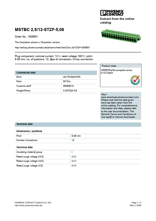
Extract from the onlinecatalogMSTBC 2,5/12-STZF-5,08Order No.: 1809831The illustration shows a 15-position versionhttp://eshop.phoenixcontact.de/phoenix/treeViewClick.do?UID=1809831Plug component, nominal current: 12 A, rated voltage: 320 V, pitch:5.08 mm, no. of positions: 12, type of connection: Crimp connectionhttp://Please note that the data givenhere has been taken from theonline catalog. For comprehensiveinformation and data, please referto the user documentation. TheGeneral Terms and Conditions ofUse apply to Internet downloads. Technical dataDimensions / positionsPitch 5.08 mmNumber of positions12Technical dataInsulating material group IRated surge voltage (III/3) 4 kVRated surge voltage (III/2) 4 kVRated surge voltage (II/2) 4 kVRated voltage (III/2)320 VRated voltage (II/2)630 VConnection in acc. with standard EN-VDENominal current I N12 ANominal voltage U N320 VNominal cross section 2.5 mm2Maximum load current12 AInsulating material PAInflammability class acc. to UL 94V0Connection dataConductor cross section stranded min.0.5 mm2Conductor cross section stranded max. 2.5 mm2Conductor cross section AWG/kcmil min.20Conductor cross section AWG/kcmil max14Certificates / ApprovalsApproval logoCSANominal voltage U N300 VNominal current I N10 AAWG/kcmil20-14CULNominal voltage U N300 VNominal current I N10 AAWG/kcmil20-14ULNominal voltage U N300 VNominal current I N10 AAWG/kcmil20-14Certification CB, CSA, CUL, UL, VDE-PZIAccessoriesItem Designation DescriptionMarking0804293SK 5,08/3,8:FORTL.ZAHLEN Marker card, printed horizontally, self-adhesive, 12 identicaldecades marked 1-10, 11-20 etc. up to 91-(99)100, sufficient for120 terminal blocksPlug/Adapter1734634CP-MSTB Coding profile, is inserted into the slot on the plug or invertedheader, red insulating material3190564MSTBC-MT 0,5-1,0Module female contact, is inserted into the plug housing MSTBCafter crimping the conductor, for conductors from 0.5 to 1.0 mm²3190645MSTBC-MT 0,5-1,0 BA Module female contact, is inserted into the MSTBC connectorshell after the conductor has been crimped, for conductors from0.5 - 1.0 mm², ribbon contact3190551MSTBC-MT 1,5-2,5Module female contact, is inserted into the plug housing MSTBCafter crimping the conductor, for conductors from 1.5 to 2.5 mm²3190658MSTBC-MT 1,5-2,5 BA Module female contact, is inserted into the MSTBC connectorshell after the conductor has been crimped, for conductors from1.5 -2.5 mm², ribbon contact1810529STZ 2-MSTBC-5,08Strain relief for snapping into the latching chambers of the plugcomponents, 2-pos., labeling with ZB 61810532STZ 4-MSTBC-5,08Strain relief for snapping into the latching chambers of the plugcomponents, 4-pos., labeling with ZB 61810516STZ 8-MSTBC-5,08Strain relief for snapping into the latching chambers of the plugcomponents, 8-pos., labeling with ZB 61810503STZ 12-MSTBC-5,08Strain relief for snapping into the latching chambers of the plugcomponents, 12-pos., labeling with ZB 6Tools1204038CRIMPFOX MT 2,5Crimping pliers, for crimping conductors to the module femalecontacts STG-MTN, crimp range: 0.5-2.5 mm², AWG: 20-14 1205037SZS 0,4X2,5Screwdriver, bladed, matches all screw terminal blocks up to 1.5mm² connection cross section, blade: 0.4 x 2.5 mm Additional productsItem Designation DescriptionGeneral1803057MSTBVK 2,5/12-GF-5,08Header, nominal current: 12 A, rated voltage: 320 V, pitch: 5.08mm, no. of positions: 12, mounting: Mounting rail1788444MVSTBU 2,5/12-GFB-5,08Header, nominal current: 12 A, rated voltage: 320 V, pitch: 5.08mm, no. of positions: 12, mounting: Direct mounting3002034UK 3-MSTB-5,08Modular terminal blocks with plug entry, cross section: 0.2 - 2.5mm², AWG: 30 - 12, width: 5.1 mm, color: gray3002076UK 3-MVSTB-5,08Modular terminal blocks with plug entry, cross section: 0.2 - 2.5mm², AWG: 26 - 12, width: 5.1 mm, color: gray3002102UK 3-MVSTB-5,08-LA 24RD Modular terminal block with plug entry, nominal current: 12 A,rated voltage: 320 V, pitch: 5.08 mm, no. of positions: 1, mounting:mounting rail, with red light indicator, voltage light indicator: 24 VAC/DC, current light indicator: 3.3 mA3002063UK 3-MVSTB-5,08/EK Modular terminal blocks with plug entry, cross section: 0.2-2.5mm², AWG: 26-12, width: 5.1 mm, color: blue3002131UK 3D-MSTBV-5,08Modular terminal blocks with vertical plug entry, cross section: 0.2- 2.5 mm, AWG: 30 - 12, width: 5.1 mm, color: gray3002144UK 3D-MSTBV-5,08-LA 24RD Modular terminal block with vertical plug entry, color: Gray, withred light indicator, voltage light indicator: 24 V AC/DC, current lightindicator: 3.3 mA3002173UK 3D-MSTBV-5,08/EK Modular terminal blocks with plug entry, cross section: 0.2 - 2.5mm², AWG: 30 - 12, width: 5.1 mm, color: blue2770888UKK 3-MSTB-5,08Modular terminal blocks with 2 horizontal plug entries, crosssection: 0.2 - 2.5 mm, AWG: 30 - 12, width: 5.1 mm, color: gray 1876615UKK 3-MSTB-5,08-PE Ground terminal block, with 2 horizontal plug entries, nominalcurrent: 12 A, rated voltage: 320 V, pitch: 5.08 mm, no. ofpositions: 1, mounting: mounting rail.1788020UMSTBVK 2,5/12-GF-5,08Header, nominal current: 12 A, rated voltage: 320 V, pitch: 5.08mm, no. of positions: 12, mounting: Mounting rail1873016ZFKK 1,5-MSTBV-5,08Modular terminal blocks with plug entry, cross section: 0.2 - 1.5mm², width: 5.1 mm, color: grayDrawingsDimensioned drawingAddressPHOENIX CONTACT GmbH & Co. KGFlachsmarktstr. 832825 Blomberg,GermanyPhone +49 5235 3 00Fax +49 5235 3 41200http://www.phoenixcontact.de© 2008 Phoenix ContactTechnical modifications reserved;。
5554434-1中文资料

5554434-1 Product DetailsHome | Customer Support | Suppliers | Site Map | Privacy Policy | Browser Support© 2008 Tyco Electronics Corporation All Rights Reserved SearchProducts Documentation Resources My Account Customer Support Home > Products > By Type > CHAMP Connectors > Product Feature Selector > Product Details5554434-1Active 2.16 [.085] IDC ConnectorsAlways EU RoHS/ELV Compliant (Statement of Compliance)Product Highlights:?Connector?Number of Positions = 24?Receptacle?Shielded?With Panel AttachmentView all Features | Find SimilarProductsCheck Pricing &AvailabilitySearch for ToolingProduct FeatureSelectorContact Us AboutThis ProductQuick LinksDocumentation & Additional InformationProduct Drawings:?EMI RECEPTACLE ASSEMBLY, 24 POSITION, LOW PROFILE SH...(PDF, English)Catalog Pages/Data Sheets:?None AvailableProduct Specifications:?None AvailableApplication Specifications:?None AvailableInstruction Sheets:?None AvailableCAD Files: (CAD Format & Compression Information)?2D Drawing (DXF, Version O1)?3D Model (IGES, Version O1)?3D Model (STEP, Version O1)List all Documents Additional Information:?Product Line InformationRelated Products:?ToolingProduct Features (Please use the Product Drawing for all design activity)Product Type Features:?Product Type = Connector?Number of Positions = 24?Gender = Receptacle?Shielded = Yes?Mating Connector Lock = With?Mating Connector Lock Type = Screwlocks?Wire/Cable Type = Ribbon Cable?Profile = Standard?Screw Size = 6-32?Shield Material = Die Cast Metal?Boss on Shield = With?Strain Relief Clip Material = Thermoplastic?Color = Black?Comment = Boss is a 1.02 [.040] shoulder onfront of shield.Mechanical Attachment:?Panel Attachment = WithTermination Related Features:?Solder Tail Contact Plating = Gold Flash overNickelBody Related Features:?Ribbon Cable Centerline Spacing (mm [in]) =1.27 [0.050]?Shield Plating = Nickel Contact Related Features:?Contact Mating Area Plating Material = GoldFlash over Palladium Nickel over Nickel, Goldover Nickel?Contact Material = Copper AlloyHousing Related Features:?Housing Material = ThermoplasticIndustry Standards:?RoHS/ELV Compliance = RoHS compliant, ELVcompliant?Lead Free Solder Processes = Not relevant forlead free process?RoHS/ELV Compliance History = Always wasRoHS compliantOperation/Application:?Application = Interface Bus Application perIEEE-488Packaging Related Features:?Packaging Method = PreassembledOther:?Brand = AMPProvide Website Feedback | Contact Customer Support。
1928437资料
PHOENIX CONTACT GmbH & Co. KGPage 1 / 2http://www.phoenixcontact.deApr 12, 2008
Extract from the onlinecatalog FBSK 10-10Order No.: 1928437http://eshop.phoenixcontact.de/phoenix/treeViewClick.do?UID=1928437
Bridge, fully insulated, pitch 10 mm, 10-pos. Commercial dataEAN4017918613792Pack50 Pcs.Customs tariff85389099Weight/Piece0.01141 KGCatalog page informationPage 460 (CC-2007)
Product notesWEEE/RoHS-compliant since:01/01/2003
http://www.download.phoenixcontact.comPlease note that the data givenhere has been taken from theonline catalog. For comprehensiveinformation and data, please referto the user documentation. TheGeneral Terms and Conditions ofUse apply to Internet downloads.
元器件交易网www.cecb2b.comFBSK 10-10Order No.: 1928437
http://eshop.phoenixcontact.de/phoenix/treeViewClick.do?UID=1928437
PHOENIX CONTACT GmbH & Co. KGPage 2 / 2http://www.phoenixcontact.deApr 12, 2008
1.5KE36A,TVS瞬变二极管中文资料
1.5KE36A,TVS瞬变二极管中文资料POWER: 1500Wa t VOLTAGE RANGE: 6.8 - 440 VAXIAL LEADED TRANSIENT VOLTAGE SUPPRESS DIODE1.5KE6.8A(CA) - 1.5KE440A(CA)6.8V – 440V Standoff VoltageCase: JEDEC DO-201AD Molded Plastic FeaturesGlass Passivated Die Construction Uni- and Bi-Directional Versions Available Excellent Clamping Capability Fast Response TimePlastic Case Material has UL FlammabilityMechanical DataTerminals: Axial Leads, Solderable per MIL-STD-202, Method 208 Polarity: Cathode Band or Cathode Notch Marking: Unidirectional – Device Code and Cathode Band Bidirectional – Device Code OnlyMaximum Ratings and Electrical Characteristics@T A =25°C unless otherwise specifiedCharacteristicSymbol ValueUnit Peak Pulse Power Dissipation at T A = 25°C (Note 1, 2, 5) Figure 3P PPM 1500 MinimumW Peak Forward Surge Current (Note 3)I FSM 200A Peak Pulse Current on 10/1000μS Waveform (Note 1) Figure 1I PPM See Table 1A Steady State Power Dissipation (Note 2, 4)P M(AV) 5.0W Operating and Storage Temperature RangeT j , T STG-65 to +175°CNote: 1. Non-repetitive current pulse, per Figure 1 and derated above T A = 25°C per Figure 4.2. Mounted on 40mm 2 copper pad.3. 8.3ms single half sine-wave duty cycle = 4 pulses per minutes maximum.4. Lead temperature at 75°C = T L .5. Peak pulse power waveform is 10/1000μS.Weight: 1.20 grams (approx.)!94.085.57.0211.4510.513.4 1.5KE440CA1.5KE400CA 1.5KE350A 1.5KE220CA 1.5KE170CA 1.5KE150A 1.5KE82CA (uA)R RMW RMW@V leakage Reverse CurrentPulse Peak (A)Vc(V)(mA)BR MAX Current********************************(V)(BI)(Uni)Voltage Stand-Off Reverse Maximum Clamping V T PP(V)V @I Volgtage Breakdown Test (V)V T Volgtage @I PP 1.5KE62CA 1.5KE56CA 1.5KE51CA 1.5KE47CA 1.5KE43CA 1.5KE39CA 1.5KE36CA 1.5KE33CA 1.5KE30CA 1.5KE27CA 1.5KE24CA 1.5KE22CA 1.5KE20CA 1.5KE18CA 1.5KE16CA 1.5KE15CA 1.5KE13CA 1.5KE12CA 1.5KE11CA 1.5KE10CA 1.5KE9.1CA 1.5KE8.2CA 1.5KE7.5CA 1.5KE6.8CA 1.5KE6.8A 1.5KE7.5A 1.5KE8.2A 1.5KE9.1A 1.5KE10A 1.5KE11A 1.5KE12A 1.5KE13A 1.5KE15A 1.5KE16A 1.5KE18A 1.5KE20A 1.5KE22A 1.5KE24A 1.5KE27A 1.5KE30A 1.5KE33A 1.5KE36A 1.5KE39A1.5KE43A 1.5KE47A 1.5KE51A 1.5KE56A 1.5KE300CA 1.5KE250CA 1.5KE200CA 1.5KE180CA 1.5KE160CA 1.5KE150CA 1.5KE130CA 1.5KE120CA 1.5KE110CA 1.5KE100CA 1.5KE91CA 1.5KE75CA 1.5KE68CA 1.5KE62A 1.5KE68A 1.5KE75A 1.5KE82A 1.5KE91A 1.5KE100A 1.5KE110A 1.5KE120A 1.5KE130A 1.5KE160A 1.5KE170A 1.5KE180A 1.5KE200A 1.5KE220A 1.5KE250A 1.5KE300A 1.5KE400A 1.5KE440A1.5KE350CA 5.80 6.45 7.14 10 144.8 1000.06.407.13 7.88 10 11.3 134.5 500.0 7.79 8.61 10 12.1 125.6 200.0 7.78 8.65 9.55 1.0 113.4 50.0 8.55 9.50 10.5 1.0 14.5 104.8 10.0 9.40 10.11.6 1.0 15.6 97.4 5.0 10.212.6 1.0 16.7 91.0 5.011.1 12.4 13.7 1.0 18.2 83.5 5.0 12.8 14.3 15.8 1.0 21.2 71.75.013.615.2 16.8 1.0 22.5 67.6 5.0 15.3 17.1 18.9 1.0 25.2 60.3 5.0 17.119.0 21.0 1.0 27.7 54.9 5.0 18.820.923.1 1.0 30.6 49.7 5.020.5 22.8 25.2 1.0 33.2 45.8 5.023.1 25.7 28.4 1.0 37.5 40.5 5.0 25.6 28.5 31.5 1.0 41.4 36.7 5.0 28.2 31.4 34.7 1.0 45.7 33.3 5.030.8 34.2 37.8 1.0 49.9 30.5 5.033.3 37.1 41.0 1.0 53.9 28.2 5.0 36.8 40.9 45.2 1.0 59.3 25.6 5.0 40.2 44.7 49.4 1.0 64.8 23.5 5.0 43.648.553.6 1.0 70.1 21.7 5.047.8 53.2 58.8 1.0 77.0 19.7 5.053.0 58.9 65.1 1.0 85.0 17.9 5.058.1 64.6 71.4 1.0 92.0 16.5 5.0 64.1 71.3 78.8 1.0 103 14.8 5.0 70.1 77.9 86.1 1.0 113 13.5 5.0 77.8 86.5 95.5 1.0 125 12.2 5.095.0 105 1.0 137 11.1 5.0105 116 1.0 152 10.0 5.0102 114 126 1.0 165 9.2 5.0 111 124 137 1.0 179 8.5 5.0128 143 158 1.0 207 7.3 5.0136 152 168 1.0 219 6.9 5.0 145 162 179 1.0 234 6.5 5.0 154 171 189 1.0 246 6.2 5.0 171 190 210 1.0 274 5.5 5.0 185 209 231 1.0 328 4.6 5.0 214 237 263 1.0 344 4.4 5.0256 285 315 1.0 414 3.7 5.0300 333 368 1.0 482 3.2 5.0 342 380 420 1.0 548 2.8 5.0 376 418 462 1.0 600 2.5 5.0TYPE255075100125150175200100755025T ,AMBIENT TEMPERATURE (°C)Fig.4Pulse Derating CurveA P K P U L S E D E R A T I N G (%P K P W R O R C U R R E N T )25507510012515017520002.55.0T ,LEAD TEMPERATURE (°C)Fig.5,Steady State Power Derating LP ,S T E A D Y S T A T E P O W E R D I S S I P A T I O N (W )d 0.11.0T ,PULSE WIDTH (μs)Fig.3Pulse Rating Curvep 0.1101001.010100100010000P ,P E A K P U L S E P O W E R (k W )P 0123I ,P E A K P U L S E C U R R E N T (%) P p pt,TIME (ms)Fig.1Pulse Waveform110100100010100100010,000V ,REVERSE STANDOFF VOLTAGE (V) Fig.2Typical Junction CapacitanceRWM C ,C A P A C I T A N C E (p F ) j。
1874125资料
Extract from the onlinecatalogFKCVR 2,5/ 4-STF-5,08Order No.: 1874125The figure shows a 10-position version of the producthttp://eshop.phoenixcontact.de/phoenix/treeViewClick.do?UID=1874125Plug component, nominal current: 12 A, rated voltage: 250 V, pitch: 5.08 mm, no. of positions: 4, type of connection: Spring-cage connectionhttp://Please note that the data givenhere has been taken from theonline catalog. For comprehensiveinformation and data, please referto the user documentation. TheGeneral Terms and Conditions ofUse apply to Internet downloads. Technical dataDimensions / positionsPitch 5.08 mmDimension a15.24 mmNumber of positions4Technical dataInsulating material group IRated surge voltage (III/3) 4 kV Rated surge voltage (III/2) 4 kV Rated surge voltage (II/2) 4 kV Rated voltage (III/2)320 V Rated voltage (II/2)630 V Connection in acc. with standard EN-VDE Nominal current I N12 A Nominal voltage U N250 V Nominal cross section 2.5 mm2 Maximum load current12 A Insulating material PA Inflammability class acc. to UL 94V0 Internal cylindrical gage A2 Stripping length10 mmConnection dataConductor cross section solid min.0.2 mm2 Conductor cross section solid max. 2.5 mm2 Conductor cross section stranded min.0.2 mm2 Conductor cross section stranded max. 2.5 mm2 Conductor cross section stranded, with ferrule0.25 mm2 without plastic sleeve min.Conductor cross section stranded, with ferrule2.5 mm2 without plastic sleeve max.Conductor cross section stranded, with ferrule0.25 mm2 with plastic sleeve min.Conductor cross section stranded, with ferrule2.5 mm2 with plastic sleeve max.Conductor cross section AWG/kcmil min.24 Conductor cross section AWG/kcmil max122 conductors with same cross section, stranded,0.5 mm2 TWIN ferrules with plastic sleeve, min.2 conductors with same cross section, stranded,1.5 mm2 TWIN ferrules with plastic sleeve, max.Certificates / ApprovalsApproval logoCULNominal voltage U N300 VNominal current I N10 AAWG/kcmil26-12ULNominal voltage U N300 VNominal current I N10 AAWG/kcmil26-12Certification CB, CUL, GOST, UL, VDE-PZIAccessoriesItem Designation DescriptionAssembly1876880STZ 8-FKC-5,08Strain relief for snapping into the latching chambers of the plugcomponents, 8-pos.1876877STZ 4-FKC-5,08Strain relief for snapping into the latching chambers of the plugs,4-pos.Marking0804293SK 5,08/3,8:FORTL.ZAHLEN Marker card, printed horizontally, self-adhesive, 12 identicaldecades marked 1-10, 11-20 etc. up to 91-(99)100, sufficient for120 terminal blocksPlug/Adapter1734634CP-MSTB Coding profile, is inserted into the slot on the plug or invertedheader, red insulating material0201744MPS-MT Test plug, consisting of: Metal part for 2.3 mm diameter sockethole0201647RPS Reducing plug, for transition from 4 mm diameter test plug socket,insulation: grayTools1205053SZS 0,6X3,5Screwdriver, bladed, matches all screw terminal blocks up to 4.0mm² connection cross section, blade: 0.6 x 3.5 mm, without VDEapprovalAdditional productsItem Designation DescriptionGeneral1842380MDSTB 2,5/ 4-GF-5,08Header, nominal current: 10 A, rated voltage: 250 V, pitch: 5.08mm, no. of positions: 4, mounting: Soldering1776524MSTB 2,5/ 4-GF-5,08Header, nominal current: 12 A, rated voltage: 250 V, pitch: 5.08mm, no. of positions: 4, mounting: Soldering1788978MSTBVK 2,5/ 4-GF-5,08Header, nominal current: 12 A, rated voltage: 320 V, pitch: 5.08mm, no. of positions: 4, mounting: Mounting rail1788363MVSTBU 2,5/ 4-GFB-5,08Header, nominal current: 12 A, rated voltage: 320 V, pitch: 5.08mm, no. of positions: 4, mounting: Direct mounting3002076UK 3-MVSTB-5,08Modular terminal blocks with plug entry, cross section: 0.2 - 2.5mm², AWG: 26 - 12, width: 5.1 mm, color: gray3002102UK 3-MVSTB-5,08-LA 24RD Modular terminal block with plug entry, nominal current: 12 A,rated voltage: 320 V, pitch: 5.08 mm, no. of positions: 1, mounting:mounting rail, with red light indicator, voltage light indicator: 24 VAC/DC, current light indicator: 3.3 mA3002063UK 3-MVSTB-5,08/EK Modular terminal blocks with plug entry, cross section: 0.2-2.5mm², AWG: 26-12, width: 5.1 mm, color: blue3002131UK 3D-MSTBV-5,08Modular terminal blocks with vertical plug entry, cross section: 0.2- 2.5 mm, AWG: 30 - 12, width: 5.1 mm, color: gray3002144UK 3D-MSTBV-5,08-LA 24RD Modular terminal block with vertical plug entry, color: Gray, withred light indicator, voltage light indicator: 24 V AC/DC, current lightindicator: 3.3 mA3002173UK 3D-MSTBV-5,08/EK Modular terminal blocks with plug entry, cross section: 0.2 - 2.5mm², AWG: 30 - 12, width: 5.1 mm, color: blue1787940UMSTBVK 2,5/ 4-GF-5,08Header, nominal current: 12 A, rated voltage: 320 V, pitch: 5.08mm, no. of positions: 4, mounting: Mounting rail1873016ZFKK 1,5-MSTBV-5,08Modular terminal blocks with plug entry, cross section: 0.2 - 1.5mm², width: 5.1 mm, color: grayDrawings Dimensioned drawingAddressPHOENIX CONTACT GmbH & Co. KGFlachsmarktstr. 832825 Blomberg,GermanyPhone +49 5235 3 00Fax +49 5235 3 41200http://www.phoenixcontact.de© 2008 Phoenix ContactTechnical modifications reserved;。
FAN8024BD中文资料
I/O
Pin Function Description
I
CH1 input
- Connection with capacitor
- for CH1
I
OP-AMP CH2 input(+)
I
OP-AMP CH2 input(-)
O OP-AMP CH2 output
I
Feedback for CH1
- Signal Vcc
O Drive3 Output (-)
- Power Ground 2
- Feedback for CH4
- Power Supply 2
- Vcc ground
I
CH3 input
- Connection with capacitor
- for CH4
I
CH4 input
I
Bias voltage input
3. Separation Of Power Supply
Pin Number 1 2 3 4 5 6 7 8 9 10 11 12 13 14 15 16 17 18 19 20 21 22 23 24 25 26 27 28
Pin Name IN1
CAP1.1 CAP1.2
IN2.1 IN2.2 OUT2 FB1 VCC PVCC1 PGND1 DO2− DO2+ DO1− DO1+ DO4+ DO4− DO3+ DO3− PGND2 FB4 PVCC2 VCCGND IN3 CAP4.2 CAP4.1 IN4 REF STBY
TSTG
NOTE: 1. When mounted on a 50mm × 50mm × 1mm PCB (Phenolic resin material). 2. Power dissipation is reduced by -13.6mW/°C above Ta = 25°C 3. Should not exeed Pd(Power dissipation) and SOA(Safe operating area).
- 1、下载文档前请自行甄别文档内容的完整性,平台不提供额外的编辑、内容补充、找答案等附加服务。
- 2、"仅部分预览"的文档,不可在线预览部分如存在完整性等问题,可反馈申请退款(可完整预览的文档不适用该条件!)。
- 3、如文档侵犯您的权益,请联系客服反馈,我们会尽快为您处理(人工客服工作时间:9:00-18:30)。
Extract from the online
catalog
MDSTBW 2,5/ 2-G
Order No.: 1802443
The figure shows a 10-position version of the product
http://eshop.phoenixcontact.de/phoenix/treeViewClick.do?UID=1802443
Header, nominal current: 10 A, rated voltage: 250 V, pitch: 5.0 mm, no. of positions: 2, mounting: Soldering
http://
Please note that the data given
here has been taken from the
online catalog. For comprehensive
information and data, please refer
to the user documentation. The
General Terms and Conditions of
Use apply to Internet downloads. Technical data
Dimensions / positions
Pitch 5 mm
Dimension a 5 mm
Number of positions2
Pin dimensions 1 x 1 mm
Hole diameter 1.4 mm
Technical data
Insulating material group I
Rated surge voltage (III/3) 4 kV
Rated surge voltage (III/2) 4 kV
Rated surge voltage (II/2) 4 kV
Rated voltage (III/2)320 V
Rated voltage (II/2)400 V
Connection in acc. with standard EN-VDE
Nominal current I N10 A
Nominal voltage U N250 V
Maximum load current10 A
Insulating material PBT
Inflammability class acc. to UL 94V0
Certificates / Approvals
Approval logo
CSA
Nominal voltage U N300 V
Nominal current I N10 A
CUL
Nominal voltage U N300 V
Nominal current I N10 A
UL
Nominal voltage U N300 V
Nominal current I N10 A
Certification CB, CSA, CUL, GOST, UL, VDE-PZI
Accessories
Item Designation Description
Assembly
1767766MDSTBW 2,5-AS Ejectors, for assembly on each side of the header
1755477MSTB-BL Keying cap, for forming sections, plugs onto header pin, green
insulating material
Marking
0804183SK 5/3,8:FORTL.ZAHLEN Marker card, printed horizontally, self-adhesive, 12 identical
decades marked 1-10, 11-20 etc. up to 91-(99)100, sufficient for
120 terminal blocks
Plug/Adapter
1734401CR-MSTB Coding section, inserted into the recess in the header or the
inverted plug, red insulating material
Additional products
Item Designation Description
Assembly
1909210FKCT 2,5/ 2-ST Plug component, nominal current: 12 A, rated voltage: 250 V,
pitch: 5.0 mm, no. of positions: 2, type of connection: Spring-cage
connection
General
1910351FKC 2,5/ 2-ST Plug component, nominal current: 12 A, rated voltage: 250 V,
pitch: 5.0 mm, no. of positions: 2, type of connection: Spring-cage
connection
1909715FKCVR 2,5/ 2-ST Plug component, nominal current: 12 A, rated voltage: 250 V,
pitch: 5.0 mm, no. of positions: 2, type of connection: Spring-cage
connection
1910034FKCVW 2,5/ 2-ST Plug component, nominal current: 12 A, rated voltage: 250 V,
pitch: 5.0 mm, no. of positions: 2, type of connection: Spring-cage
connection
1779411FRONT-MSTB 2,5/ 2-ST Plug component, nominal current: 12 A, rated voltage: 250 V,
pitch: 5.0 mm, no. of positions: 2, type of connection: Screw
connection
1754449MSTB 2,5/ 2-ST Plug component, nominal current: 12 A, rated voltage: 250 V,
pitch: 5.0 mm, no. of positions: 2, type of connection: Screw
connection
1765771MSTBP 2,5/ 2-ST Plug component, nominal current: 12 A, rated voltage: 250 V,
pitch: 5.0 mm, no. of positions: 2, type of connection: Screw
connection
1779835MSTBT 2,5/ 2-ST Plug component, nominal current: 12 A, rated voltage: 250 V,
pitch: 5.0 mm, no. of positions: 2, type of connection: Screw
connection
1792016MVSTBR 2,5/ 2-ST Plug component, nominal current: 12 A, rated voltage: 250 V,
pitch: 5.0 mm, no. of positions: 2, type of connection: Screw
connection
1792524MVSTBW 2,5/ 2-ST Plug component, nominal current: 12 A, rated voltage: 250 V,
pitch: 5.0 mm, no. of positions: 2, type of connection: Screw
connection
1768765SMSTB 2,5/ 2-ST Plug component, nominal current: 12 A, rated voltage: 250 V,
pitch: 5.0 mm, no. of positions: 2, type of connection: Screw
connection
Drawings
Drilling diagram
Dimensioned drawing
Address
PHOENIX CONTACT GmbH & Co. KG
Flachsmarktstr. 8
32825 Blomberg,Germany
Phone +49 5235 3 00
Fax +49 5235 3 41200
http://www.phoenixcontact.de
© 2008 Phoenix Contact
Technical modifications reserved;。