MAX309EPE+中文资料
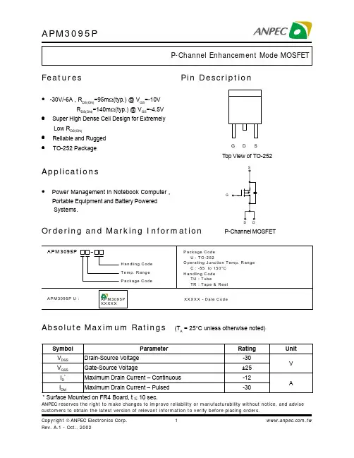
APM3095P中文资料
RDS(ON)-On-Resistance (Ω)
On-Resistance vs. Drain Current
0.24
0.21
0.18 -VGS=4.5V
0.15
0.12 -VGS=10V
0.09
0.06
0.03
0.00 012345678
-VSD -Source-to-Drain Voltage (V)
Power (W)
Single Pulse Power
250
200
150
100
50
0 1E-3 0.01
0.1 1 10
Time (sec)
100 1000
Normalized Effective Transient Thermal Impedance
2.18
2.39
0.89
1.27
0.508
0.89
5.207
5.461
0.46
0.58
0.46
0.58
5.334
6.22
6.35
6.73
3.96
5.18
9.398
10.41
0.51
0.64
1.02
0.89
2.032
Copyright ANPEC Electronics Corp.
6
Rev. A.1 - Oct., 2002
Symbol PD
TJ TSTG RθjA
Parameter Maximum Power Dissipation TA=25°C
TA=100°C Maximum Junction Temperature Storage Temperature Range Thermal Resistance – Junction to Ambient
MAX1239MEEE中文资料
Stresses beyond those listed under “Absolute Maximum Ratings” may cause permanent damage to the device. These are stress ratings only, and functional operation of the device at these or any other conditions beyond those indicated in the operational sections of the specifications is not implied. Exposure to absolute maximum rating conditions for extended periods may affect device reliability.
MAX1236–MAX1239
♦ ♦
Applications
Hand-Held Portable Applications Medical Instruments Battery-Powered Test Equipment Solar-Powered Remote Systems Received-Signal-Strength Indicators System Supervision
________________________________________________________________ Maxim Integrated Products
For pricing, delivery, and ordering information, please contact Maxim/Dallas Direct! at 1-888-629-4642, or visit Maxim’s website at .
MAX3095ESE+中文资料
________________________Applications
Telecommunications Equipment Rugged RS-422/RS-485/RS-423 Bus Receiver Receivers for ESD-Sensitive Applications Level Translators
Stresses beyond those listed under “Absolute Maximum Ratings” may cause permanent damage to the device. These are stress ratings only, and functional operation of the device at these or any other conditions beyond those indicated in the operational sections of the specifications is not implied. Exposure to absolute maximum rating conditions for extended periods may affect device reliability.
________________Functional Diagram
VCC
Байду номын сангаасG G A1
MAX3095 MAX3096
Y1
Pin Configuration
TOP VIEW
B1 1 A1 2 Y2 Y1 3 G 4 Y3 Y2 5 A2 6 Y4 B2 7 GND 8 16 VCC 15 B4 14 A4
For pricing, delivery, and ordering information, please contact Maxim/Dallas Direct! at 1-888-629-4642, or visit Maxim’s website at .
MAX2605-MAX2609中文资料
General DescriptionThe MAX2605–MAX2609 evaluation kits (EV kits) simplify evaluation of this family of voltage-controlled oscillators (VCOs). These kits enable testing of the devices’ per-formance and require no additional support circuitry.Both signal outputs use SMA connectors to facilitate connection to RF test equipment.These EV kits are fully assembled and tested. Their oscil-lation frequencies are set to approximately the midrange of the respective VCOs.Featureso Easy Evaluationo Complete, Tunable VCO Test Board with Tank Circuit o Low Phase Noiseo Fully Assembled and TestedEvaluate: MAX2605–MAX2609MAX2605–MAX2609 Evaluation Kits19-1673 Rev 0; 9/00Ordering InformationComponent SuppliersFor free samples and the latest literature, visit or phone 1-800-998-8800.For small orders, phone 1-800-835-8769.MAX2606 Component ListMAX2605 Component ListE v a l u a t e : M A X 2605–M A X 2609MAX2605–MAX2609 Evaluation Kits 2_______________________________________________________________________________________Quick StartThe MAX2605–MAX2609 evaluation kits are fully assembled and factory tested. Follow the instructions in the Connections a nd Setup section for proper device evaluation.Test Equipment Required•Low-noise power supplies (these are recommended for oscillator noise measurement). Noise or ripple will frequency-modulate the oscillator and cause spectral spreading. Batteries can be used in place of power supplies, if necessary.– Use a DC power supply capable of supplying +2.7V to +5.5V. Alternatively, use two or three 1.5V batteries.– Use a DC power supply capable of supplying +0.4V to +2.4V, continuously variable, for TUNE.Alternatively, use two 1.5V batteries with a resistive voltage divider or potentiometer.•An RF spectrum analyzer that covers the operating frequency range of the MAX2605–MAX2609• A 50Ωcoaxial cable with SMA connectors •An ammeter (optional)Connections and Setup1)Connect a DC supply (preset to +3V) to the V CC and GND terminals (through an ammeter, if desired) on the EV kit.2)Turn on the DC supply. If used, the ammeter readingMAX2607 Component ListMAX2608 Component ListEvaluate: MAX2605–MAX2609MAX2605–MAX2609 Evaluation Kits_______________________________________________________________________________________3approximates the typical operating current specified in the MAX2605–MAX2609 data sheet.3)Connect the VCO output (OUT+ or OUT-) to a spec-trum analyzer with a 50Ωcoaxial cable.4)Apply a positive variable DC voltage between 0.4V and 2.4V to TUNE.5)Check the tuning bandwidth on the spectrum analyz-er by varying the tuning voltage (+0.4V to +2.4V).Layout ConsiderationsThe EV kit PC board can serve as a guide for laying out a board using the MAX2605–MAX2609. Generally, the VCC pin on the PC board should have a decoupling capacitor placed close to the IC. This minimizes noisecoupling from the supply. Also, place the VCO as far away as possible from the noisy section of a larger sys-tem, such as a switching regulator or digital circuits.The VCO ’s performance is strongly dependent on the availability of the external tuning inductor. For best per-formance, use high-Q components and choose their val-ues carefully. To minimize the effects of parasitic ele-ments, which degrade circuit performance, place the tuning inductor and C BYP close to the VCO. For higher-frequency versions, include the parasitic PC board inductance and capacitance when calculating the oscillation frequency. In addition, remove the ground plane around and under the tuning inductor to minimize the effect of parasitic capacitance.Noise on TUNE translates into FM noise on the outputs;therefore, keep the trace between TUNE and the control circuitry as short as possible. If necessary, use an RC filter to further suppress noise, as done on the EV kits.E v a l u a t e : M A X 2605–M A X 2609MAX2605–MAX2609 Evaluation Kits 4_______________________________________________________________________________________Figure 2. MAX2608/MAX2609 EV Kits SchematicFigure 1. MAX2605/MAX2606/MAX2607 EV Kits SchematicEvaluate: MAX2605–MAX2609MAX2605–MAX2609 Evaluation Kits_______________________________________________________________________________________5Figure 3. MAX2605/MAX2606/MAX2607 EV Kits ComponentPlacement Guide—Top Silk ScreenFigure 4. MAX2608/MAX2609 EV Kits Component PlacementGuide—Top Silk ScreenFigure 5. MAX2605/MAX2606/MAX2607 EV Kits PC BoardLayout—Component SideFigure 6. MAX2608/MAX2609 EV Kits PC Board Layout—Component SideMa xim ca nnot a ssume responsibility for use of a ny circuitry other tha n circuitry entirely embodied in a Ma xim product. No circuit pa tent licenses a re implied. Maxim reserves the right to change the circuitry and specifications without notice at any time.6_____________________Maxim Integrated Products, 120 San Gabriel Drive, Sunnyvale, CA 94086 408-737-7600©2000 Maxim Integrated ProductsPrinted USAis a registered trademark of Maxim Integrated Products.E v a l u a t e : M A X 2605–M A X 2609MAX2605–MAX2609 Evaluation Kits Figure 7. MAX2605/MAX2606/MAX2607/MAX2608/MAX2609EV Kits PC Board Layout—Ground Plane。
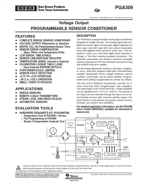
PGA309资料
proper handling and installation procedures can cause damage. ESD damage can range from subtle performance degradation to complete device failure. Precision integrated circuits may be more susceptible to damage because very small parametric changes could1s/divV REF =4.096VMeasured After Bandpass Filter 0.1Hz Second−Order High−Pass 10Hz Fourth−Order Low−Pass1s/divG =1152Coarse Offset =−59mVMeasured After Bandpass Filter 0.1Hz Second−Order High−Pass 10Hz Fourth−Order Low−PassV IN =+61mVCLK_CFG=00(default)Gain=1152Time(10µs/div)SMALL−SIGNAL STEP RESPONSEGain=256Time(10µs/div)OVERVOLTAGE RECOVERYV OUTUnit1 Unit2Code(LSB)70000100002000030000400006000050000vs CODEPACKAGING INFORMATIONOrderable Device Status (1)Package Type Package Drawing Pins Package Qty Eco Plan (2)Lead/Ball FinishMSL Peak Temp (3)PGA309AIPWR ACTIVE TSSOP PW 162500Green (RoHS &no Sb/Br)CU SNPB Level-1-260C-UNLIM PGA309AIPWTACTIVETSSOPPW16250Green (RoHS &no Sb/Br)CU SNPBLevel-1-260C-UNLIM(1)The marketing status values are defined as follows:ACTIVE:Product device recommended for new designs.LIFEBUY:TI has announced that the device will be discontinued,and a lifetime-buy period is in effect.NRND:Not recommended for new designs.Device is in production to support existing customers,but TI does not recommend using this part in a new design.PREVIEW:Device has been announced but is not in production.Samples may or may not be available.OBSOLETE:TI has discontinued the production of the device.(2)Eco Plan -May not be currently available -please check /productcontent for the latest availability information and additional product content details.None:Not yet available Lead (Pb-Free).Pb-Free (RoHS):TI's terms "Lead-Free"or "Pb-Free"mean semiconductor products that are compatible with the current RoHS requirements for all 6substances,including the requirement that lead not exceed 0.1%by weight in homogeneous materials.Where designed to be soldered at high temperatures,TI Pb-Free products are suitable for use in specified lead-free processes.Green (RoHS &no Sb/Br):TI defines "Green"to mean "Pb-Free"and in addition,uses package materials that do not contain halogens,including bromine (Br)or antimony (Sb)above 0.1%of total product weight.(3)MSL,Peak Temp.--The Moisture Sensitivity Level rating according to the JEDECindustry standard classifications,and peak solder temperature.Important Information and Disclaimer:The information provided on this page represents TI's knowledge and belief as of the date that it is provided.TI bases its knowledge and belief on information provided by third parties,and makes no representation or warranty as to the accuracy of such information.Efforts are underway to better integrate information from third parties.TI has taken and continues to take reasonable steps to provide representative and accurate informationbut may not have conducted destructive testing or chemical analysis on incoming materials and chemicals.TI and TI suppliers consider certain information to be proprietary,and thus CAS numbers and other limited information may not be available for release.In no event shall TI's liability arising out of such information exceed the total purchase price of the TI part(s)at issue in this document sold by TI to Customer on an annual basis.PACKAGE OPTION ADDENDUM9-Dec-2004Addendum-Page 1元器件交易网元器件交易网IMPORTANT NOTICETexas Instruments Incorporated and its subsidiaries (TI) reserve the right to make corrections, modifications,enhancements, improvements, and other changes to its products and services at any time and to discontinueany product or service without notice. Customers should obtain the latest relevant information before placingorders and should verify that such information is current and complete. All products are sold subject to TI’s termsand conditions of sale supplied at the time of order acknowledgment.TI warrants performance of its hardware products to the specifications applicable at the time of sale inaccordance with TI’s standard warranty. T esting and other quality control techniques are used to the extent TIdeems necessary to support this warranty. Except where mandated by government requirements, testing of allparameters of each product is not necessarily performed.TI assumes no liability for applications assistance or customer product design. Customers are responsible fortheir products and applications using TI components. T o minimize the risks associated with customer productsand applications, customers should provide adequate design and operating safeguards.TI does not warrant or represent that any license, either express or implied, is granted under any TI patent right,copyright, mask work right, or other TI intellectual property right relating to any combination, machine, or processin which TI products or services are used. Information published by TI regarding third-party products or servicesdoes not constitute a license from TI to use such products or services or a warranty or endorsement thereof.Use of such information may require a license from a third party under the patents or other intellectual propertyof the third party, or a license from TI under the patents or other intellectual property of TI.Reproduction of information in TI data books or data sheets is permissible only if reproduction is withoutalteration and is accompanied by all associated warranties, conditions, limitations, and notices. Reproductionof this information with alteration is an unfair and deceptive business practice. TI is not responsible or liable forsuch altered documentation.Resale of TI products or services with statements different from or beyond the parameters stated by TI for thatproduct or service voids all express and any implied warranties for the associated TI product or service andis an unfair and deceptive business practice. TI is not responsible or liable for any such statements.Following are URLs where you can obtain information on other Texas Instruments products and applicationsolutions:Products ApplicationsAmplifiers Audio /audioData Converters Automotive /automotiveDSP Broadband /broadbandInterface Digital Control /digitalcontrolLogic Military /militaryPower Mgmt Optical Networking /opticalnetworkMicrocontrollers Security /securityTelephony /telephonyVideo & Imaging /videoWireless /wirelessMailing Address:Texas InstrumentsPost Office Box 655303 Dallas, Texas 75265Copyright 2004, Texas Instruments Incorporated。
普洛麦格(北京)生物技术有限公司CTM692产品说明书

2022版 CTM692原英文技术手册TM692中 文 说 明 书适用产品目录号:GA1330和GA1332FcγRI ADCP BioassayEffector Cells, Propagation Model普洛麦格(北京)生物技术有限公司Promega (Beijing) Biotech Co., Ltd 地址:北京市东城区北三环东路36号环球贸易中心B 座907-909电话:************网址: 技术支持电话:400 810 8133技术支持邮箱:*************************CTM 6922022制作1所有技术文献的英文原版均可在/ protocols 获得。
请访问该网址以确定您使用的说明书是否为最新版本。
如果您在使用该试剂盒时有任何问题,请与Promega 北京技术服务部联系。
电子邮箱:*************************1. 描述 ....................................................................................................................................................................................22. 产品组分和储存条件............................................................................................................................................................43. 开始实验前 ..........................................................................................................................................................................54. 制备Fc γRI ADCP 效应细胞 ................................................................................................................................................6 4. A. 细胞解冻和初始细胞培养 .......................................................................................................................................... 6 4. B. Fc γRI ADCP 效应细胞的细胞维持和增殖 ..................................................................................................................7 4. C. Fc γRI ADCP 效应细胞冷冻和储存 .............................................................................................................................75. 检测方案 .............................................................................................................................................................................8 5. A. Bio-Glo™试剂、检测缓冲液和测试及对照样品的制备...............................................................................................9 5. B. 孔板布局设计 ...........................................................................................................................................................10 5. C. 检测前一天制备和铺板贴壁靶细胞 ...........................................................................................................................10 5. D. 检测当天制备悬浮靶细胞 .........................................................................................................................................11 5. E. 制备抗体系列稀释液 ................................................................................................................................................12 5. F. 制备Fc γRI 效应细胞 ................................................................................................................................................12 5. G. 铺板悬浮靶细胞、抗体和Fc γRI 效应细胞 ................................................................................................................13 5. H. 将抗体和Fc γRI 效应细胞加至预先铺板的贴壁靶细胞中 ...........................................................................................13 5. I. 加入Bio-Glo™试剂 ..................................................................................................................................................14 5. J. 数据分析...................................................................................................................................................................146. 疑难解答 ...........................................................................................................................................................................157. 参考文献 ...........................................................................................................................................................................168. 代表性检测结果.. (17)FcγRI ADCP Bioassay Effector Cells, Propagation Model普洛麦格(北京)生物技术有限公司Promega (Beijing) Biotech Co., Ltd 地址:北京市东城区北三环东路36号环球贸易中心B座907-909电话:************网址:技术支持电话:400 810 8133技术支持邮箱:*************************CTM 6922022制作21. 描述抗体依赖性细胞介导的吞噬作用(ADCP)是治疗性抗体识别和介导消除病毒性感染细胞或病变(如肿瘤)细胞的重要作用机制。
MEMORY存储芯片MAX490CPA+中文规格书
±15kV ESD-Protected, Slew-Rate-Limited, Low-Power, RS-485/RS-422 TransceiversThe major difference between tests done using the Human Body Model and IEC1000-4-2 is higher peak current in IEC1000-4-2, because series resistance is lower in the IEC1000-4-2 model. Hence, the ESD with-stand voltage measured to IEC1000-4-2 is generally lower than that measured using the Human Body Model. Figure 7 shows the current waveform for the 8kV IEC1000-4-2 ESD contact-discharge test.The air-gap test involves approaching the device with a charged probe. The contact-discharge method connects the probe to the device before the probe is energized.Machine Model The Machine Model for ESD tests all pins using a 200pF storage capacitor and zero discharge resis-tance. Its objective is to emulate the stress caused by contact that occurs with handling and assembly during manufacturing. Of course, all pins require this protec-tion during manufacturing—not just inputs and outputs. Therefore,after PC board assembly,the Machine Model is less relevant to I/O ports.MAX487E/MAX1487E:128 Transceivers on the Bus The 48kΩ, 1/4-unit-load receiver input impedance of the MAX487E and MAX1487E allows up to 128 transceivers on a bus, compared to the 1-unit load (12kΩinput impedance) of standard RS-485 drivers (32 transceivers maximum). Any combination of MAX487E/MAX1487E and other RS-485 transceivers with a total of 32 unit loads or less can be put on the bus. The MAX481E, MAX483E, MAX485E, and MAX488E–MAX491E have standard 12kΩreceiver input impedance.MAX483E/MAX487E/MAX488E/MAX489E:Reduced EMI and Reflections The MAX483E and MAX487E–MAX489E are slew-rate limited, minimizing EMI and reducing reflections caused by improperly terminated cables. F igure 16 shows the driver output waveform and its Fourier analy-sis of a 150kHz signal transmitted by a MAX481E, MAX485E, MAX490E, MAX491E, or MAX1487E. High-frequency harmonics with large amplitudes are evident.F igure 17 shows the same information displayed for a MAX483E, MAX487E, MAX488E, or MAX489E transmit-ting under the same conditions. F igure 17’s high-fre-quency harmonics have much lower amplitudes, and the potential for EMI is significantly reduced.Low-Power Shutdown Mode(MAX481E/MAX483E/MAX487E) A low-power shutdown mode is initiated by bringing both RE high and DE low. The devices will not shut down unless both the driver and receiver are disabled. In shutdown, the devices typically draw only 0.5µA of supply current.RE and DE may be driven simultaneously; the parts are guaranteed not to enter shutdown if RE is high and DE is low for less than 50ns. If the inputs are in this state for at least 600ns, the parts are guaranteed to enter shutdown.F or the MAX481E, MAX483E, and MAX487E, the t ZH and t ZL enable times assume the part was not in the low-power shutdown state (the MAX485E, MAX488E–MAX491E, and MAX1487E can not be shut down). The t ZH(SHDN)and t ZL(SHDN)enable times assume the parts were shut down (see Electrical Characteristics).Figure 16. Driver Output Waveform and FFT Plot of MAX485E/MAX490E/MAX491E/MAX1487E Transmitting a 150kHz SignalFigure 17. Driver Output Waveform and FFT Plot ofMAX483E/MAX487E–MAX489E Transmitting a 150kHz SignalMAX481E/MAX483E/MAX485E/ MAX487E–MAX491E/MAX1487E 12±15kV ESD-Protected, Slew-Rate-Limited, Low-Power, RS-485/RS-422 TransceiversOrdering Information (continued)Selector GuideChip InformationTRANSISTOR COUNT: 295MAX481E/MAX483E/MAX485E/MAX487E–MAX491E/MAX1487E。
MAX3095中文资料
MAX3095/MAX3096
_______________Ordering Information
PART MAX3095CPE MAX3095CSE MAX3095CEE MAX3095EPE MAX3095ESE MAX3095EEE MAX3096CPE MAX3096CSE MAX3096CEE MAX3096EPE MAX3096ESE MAX3096EEE TEMP. RANGE 0°C to +70°C 0°C to +70°C 0°C to +70°C -40°C to +85°C -40°C to +85°C -40°C to +85°C 0°C to +70°C 0°C to +70°C 0°C to +70°C -40°C to +85°C -40°C to +85°C -40°C to +85°C PIN-PACKAGE 16 Plastic DIP 16 Narrow SO 16 QSOP 16 Plastic DIP 16 Narrow SO 16 QSOP 16 Plastic DIP 16 Narrow SO 16 QSOP 16 Plastic DIP 16 Narrow SO 16 QSOP
±15kV ESD-Protected, 10Mbps, 3V/5V, Quad RS-422/RS-485 Receivers MAX3095/MAX3096
ABSOLUTE MAXIMUM RATINGS
Supply Voltage (VCC) ...............................................................7V Control Input Voltage (G, G).......................-0.3V to (VCC + 0.3V) Receiver Input Voltage (A_, B_)...........................................±25V Receiver Output Voltage (Y_).....................-0.3V to (VCC + 0.3V) Continuous Power Dissipation (TA = +70°C) Plastic DIP (derate 10.5mW/°C above +70°C) ............762mW SO (derate 8.7mW/°C above +70°C) ...........................696mW QSOP (derate 8.3mW/°C above +70°C) ......................667mW Operating Temperature Ranges MAX309_C_ _ .....................................................0°C to +70°C MAX309_E_ _...................................................-40°C to +85°C Storage Temperature Range .............................-65°C to +160°C Lead Temperature (soldering, 10sec) .............................+300°C
MAX3094EESE中文资料
For pricing, delivery, and ordering information, please contact Maxim/Dallas Direct! at 1-888-629-4642, or visit Maxim’s website at .
元器件交易网
MAX3093E/MAX3094E
_______________Ordering Information
PART MAX3093ECUE MAX3093ECSE MAX3093ECPE MAX3093EEUE MAX3093EESE MAX3093EEPE MAX3094ECUE MAX3094ECSE MAX3094ECPE MAX3094EEUE MAX3094EESE MAX3094EEPE TEMP RANGE 0°C to +70°C 0°C to +70°C 0°C to +70°C -40°C to +85°C -40°C to +85°C -40°C to +85°C 0°C to +70°C 0°C to +70°C 0°C to +70°C -40°C to +85°C -40°C to +85°C -40°C to +85°C PIN-PACKAGE 16 TSSOP 16 Narrow SO 16 Plastic DIP 16 TSSOP 16 Narrow SO 16 Plastic DIP 16 TSSOP 16 Narrow SO 16 Plastic DIP 16 TSSOP 16 Narrow SO 16 Plastic DIP
________________________Applications
电子芯片大全
号功能简述型号AD1380JDAD1380KDAD1671JQAD1672APAD1674ADAD1674JNAD202JNAD202JYAD204JNAD22100KTAD22105ARAD261BND-1AD2S99APAD420AN-32AD420AR-32AD421BNAD421BRAD515AJHAD515ALHAD517JHAD518JHAD521JDAD524ADAD526BDAD526JNAD532JHAD534JDAD534JHAD536AJDAD536AJHAD536AJQAD537JHAD537SHAD538ADAD539JNAD542JHAD545ALHAD546JNAD547JHAD548JNAD549JHAD549LHAD5539JNAD557JNAD558JNAD568JQ AD569JN AD570JD/+ AD574AJD AD574AKD AD578KN AD580JH AD580LH AD581JH AD582KD AD584JH AD584JN AD585AQ AD586JN AD586JQ AD586KN AD586KQ AD586KR AD587KN AD587KR AD588AQ AD589JH AD590JH AD590KH AD592AN AD592BN AD595AD AD595AQ AD598AD AD600XN AD602JN AD603AQ AD606JN AD607ARS AD620AN AD621AN AD622AN AD623AN AD623AR AD624AD AD625JN AD625KN AD626AN AD627AN AD629AN AD630JNAD636JDAD636JHAD637JQAD648JNAD650JNAD650KNAD652AQAD654JNAD654JRAD660ANAD6640AST AD6644AST AD667JNAD667KNAD669ANAD670JNAD676JDAD676JNAD676KDAD677ARAD677JDAD677JNAD678JDAD678KNAD679JNAD679KNAD680JNAD684JQAD693AQAD694AQAD694JNAD698APAD7008AP20 AD7008JP-50 AD704JNAD705JNAD706JNAD707AQAD707JNAD708AQAD708JNAD7111ABN AD7111LN AD711AQAD711JNAD711JRAD712JN AD713BQ AD713JN AD720JP AD7224KN AD7226KN AD7228ABN AD722JR-16 AD7237AAN AD7237JN AD7243AN AD7245AAN AD7249BN AD724JR AD73360AR AD734AQ AD736JN AD737AQ AD737JN AD7416AR AD741KN AD743JN AD744JN AD745JN AD75019JP AD7501JN AD7502JN AD7502KQ AD7503JN AD7506JN AD7507JN AD7510DIJN AD7510DIKN AD7512DIJN AD7512DIKN AD7520LN AD7523JN AD7524JN AD7528JN AD7528KN AD7533JN AD7535JN AD7537JN AD7541AKN AD7542JN AD7543KNAD7564BN AD7574JN AD7590DIKN AD7660AST AD7664AST AD767JNAD768ARAD7701AN AD7703AN AD7703BN AD7705BN AD7705BR AD7706BN AD7707BR AD7710AN AD7711AN AD7712AN AD7713AN AD7714AN-3 AD7714AN-5 AD7715AN-5 AD7715AR-5 AD7731BN AD7741BN AD7742BN AD7750AN AD7755AARS AD7777AR AD779JDAD780ANAD781JNAD7820KN AD7821KN AD7822BN AD7824BQ AD7824KN AD7837AN AD7845JN AD7846JN AD7847AN AD7856AN AD7862AN-10 AD7864AS-1 AD7865AS-1 AD7872AN AD7874ANAD7886JD AD7886KD AD7888AR AD7890AN-10 AD7891AP-1 AD7892AN-1 AD7895AN-10 AD790JNAD795JNAD797ANAD797ARAD8001AN AD8002AN AD8009AR AD8011AN AD8015AR AD8018AR AD8031AN AD8032AN AD8036AN AD8037AN AD8041AN AD8041AR AD8042AN AD8044AN AD8047AN AD8055AR AD8056AR AD8058AR AD8079AR AD8108AST AD8109AST AD810ANAD8111AST AD8115AST AD8116AST AD811ANAD811JRAD812ANAD812ARAD8131AR AD8138AR AD813ANAD813AR-14 AD815AYAD8170ANAD817ANAD8180AN AD8184AN AD818ANAD820ANAD822ANAD822AN-3V AD823ANAD824ANAD826ANAD827AQAD827JNAD828ANAD829JNAD8307AN AD8307AR AD8309ARU AD830ANAD830ANAD8313ARM AD8313ARM AD8320ARP AD834JNAD8350AR15 AD835ANAD8402AN-10 AD8403AN100 AD840JNAD843AQAD844ANAD845JNAD845KNAD847AQAD847JNAD847SQAD849JNAD8522AN AD8551AR AD8552AR AD8561AN AD8561AR AD8564AN AD8598AN AD9042AST AD9048JQ AD9049BRSAD9051BRSAD9057BRS-40 AD9057BRS-60 AD9058JJAD9059BRSAD9066JRAD9071BRAD9101ARAD9200ARSAD9203ARUAD9220ARAD9221ARAD9223ARAD9225ARAD9226ARSAD9240ASAD9243ASAD9260ASAD9280ARSAD9281ARSAD9283BRS-100 AD9283BRS-80 AD9288BRS-80 AD9300KQAD9483KS-100 AD9500BQAD9501JNAD9617JRAD9617JNAD9618JNAD9630ANAD9631ANAD96687BQAD9698KNAD9708ARUAD9709ASTAD9713BANAD9721BRAD9731BRAD9732BRSAD9750ARAD9752ARAD9760ARAD9762ARAD9764ARAD976CNAD976AAN AD9772AST AD977AAN AD977AN AD9801JCST AD9802JST AD9803JST AD9805JS AD9816JS AD9822JR AD9830AST AD9831AST AD9832BRU AD9850BRS AD9851BRS AD9852AST AD9852ASQ AD9853AS AD9854AST AD9854ASQ AD9901KQ ADG201AKN ADG201HSJN ADG211AKN ADG222AKN ADG333ABN ADG333ABR ADG408BN ADG409BN ADG411BN ADG417BN ADG419BN ADG431BN ADG436BN ADG441BN ADG442BN ADG506AKN ADG507AKN ADG508AKN ADG508FBN ADG509AKN ADG511BN ADG608BN ADG609BN ADG719BRM ADG736BRMADM690ANADM708ANADSP21060KS160 ADSP21060CZ-160 ADSP21062KS-160 ADSP2181KS-133 ADSP2181KST-133 ADUC812BS ADVF32KNADXL105JQC ADXL202AQC AMP02FPAMP04FPDAC08CPDAC8228FPOP07AZ/883COP07CPOP07CSOP176GPOP177GPOP27GPOP291GPOP295GPOP296GPOP297GPOP297GSOP37EPOP37GPOP495GPOP497GPOP77GPOP90GPOP97FPOP97FSPKD01FPREF02CPREF03GPREF192GPREF192GSREF194GPREF195GSREF43FZSMP04EPSMP08FPSSM2141PSSM2142PSSM2211P SSM2275P TMP03FS TMP04FS TMP36GT9 MAX038CPP MAX1044CPA MAX110ACPE MAX110BCPE MAX111BCPE MAX122BCNG MAX1232CPA MAX1242BCSA MAX125CEAX MAX134CPL MAX135CPI MAX139CPL MAX140CPL MAX1480BCPI MAX1480BEPI MAX1483CPA MAX1487CPA MAX1487ECPA MAX1488ECPD MAX1489ECPD MAX148BCPP MAX1490BCPG MAX158BCPI MAX1771CPA MAX1771CSA MAX180CCPL MAX186CCPP MAX187BCPA MAX189CCPA MAX191BCNG MAX192BCPP MAX197BCNI MAX202CPE MAX202CSE MAX202ECPE MAX202EESE MAX202EPE MAX207CNG MAX208CNG MAX232CPE MAX232CSEMAX235CPG MAX238CNG MAX238ENG MAX260BCHG MAX260BENG MAX261BCNG MAX280CPA MAX291CPA MAX292CPA MAX293CPA MAX294CPA MAX297CPA MAX301CPE MAX305EPE MAX306CPI MAX3080CPD MAX3082CPA MAX308CPE MAX309CPE MAX3100CPD MAX312CPE MAX313CPE MAX318CPA MAX319CPA MAX3218CPP MAX3223CPP MAX3232CPE MAX325CPA MAX333CPP MAX338CPE MAX339CPE MAX351CPE MAX354CPE MAX354CWE MAX354EPE MAX355CPE MAX355CWE MAX366CPA MAX367CPN MAX384CPN MAX391CPE MAX400CPA MAX4016ESA MAX4100ESA MAX4101ESA MAX4106ESAMAX4142ESD MAX4146ESD MAX419CPD MAX420CPA MAX427CPA MAX435CPD MAX436CPD MAX440CPI MAX441CPP MAX442CPA MAX4456CPL MAX453EPA MAX457EPA MAX458CPL MAX468CPE MAX470CPE MAX479CPD MAX480EPA MAX483CPA MAX485CPA MAX487CPA MAX487ECPA MAX487EEPA MAX488CPA MAX490ECPA MAX491CPD MAX491ECPD MAX501AENG MAX504CPD MAX505BCNG MAX506CPP MAX509BCPE MAX512CPD MAX515CPA MAX517BCPA MAX518BCPA MAX526DCNG MAX527DCNG MAX528CPP MAX530BCNG MAX531BCPD MAX532BCPE MAX536BCWE MAX538BCPA MAX543ACPA MAX551ACPAMAX619CPA MAX6225ACPA MAX6225AESA MAX6225BCPA MAX6225BCSA MAX622CPA MAX6250BCPA MAX633ACPA MAX638AEPA MAX639CPA MAX660CPA MAX662ACPA MAX667CPA MAX691ACPE MAX691CPE MAX705CPA MAX706CPA MAX708CPA MAX708CSA-T MAX709LEPA MAX712CPE MAX712EPE MAX713CPE MAX7219CNG MAX7219ENG MAX724CCK MAX726CCK MAX729CCK MAX730ACPA MAX733CPA MAX735CPA MAX736CPD MAX738ACPA MAX738AEPA MAX739CPD MAX739CWE MAX7400CPA MAX743CPE MAX743EPE MAX749CPA MAX750ACPA MAX756CPA MAX761CPA MAX764CPA MAX765CPA MAX766EPAMAX791CPE MAX807LCPE MAX810LEUR-T MAX813LCPA MAX813LEPA MAX818LCPA MAX860ISA MAX865EUA MAX866ESA MAX874EPA MAX875BCPA MAX882CPA MAX883CPA MAX883CSA MAX907CPA MAX910CNG MAX912CPE MAX913CPA MAX931CPA MAX934CPE MXD1210CPA LFC2LFC3LFC4LFC54LFC75F003F004(5G23)F005F006F007(5G24)F010F011F1550F1490F1590F157/AF253F741(F007)F741AF747OP-07OP111AF4741F101A/201AF301AF308F110/210 F310F118/218 F441F318F124/224 F324F148F248/348 F158/258 F358F1558F4558LF791LF4136 FD37/FD38 FD46LF082 LFOP37LF3140LF7650LZ1606LZ19001 LBMZ1901 LM741LM747OP-07LM101/201 LM301LM108/208 LM308LM110LM310LM118/218 LM318LM124/224 LM324LM148LM248/348 LM158/258 LM358LM1558 OP-27CP TL062TL072TL082TL084MC1458LF147/347LF156/256/356LF107/307LF351LF353LF155/355LF157/357LM359LM381CA3080CA3100CA3130CA3140CA3240CA3193CA3401MC3303MC3403LF411LF444µpc4558MC4741LM709LM725LM733LM748ICL7650ICL7660稳压器固定输出(正电压)稳压器78xx 系列 3端稳压器 5V 到 24V1A78Lxx 系列 3端稳压器 5V 到 24V 0.1A78Mxx 系列 3端稳压器 5V 到 24V 0.5A78Sxx 系列 3端稳压器 5V 到 24V 2A固定输出(负电压)稳压器79xx 系列 3端负电压稳压器 -5V 到 -24V 1A [110kb] 79Lxx 系列 3端负电压稳压器 -5V 到 -24V 0.1A [95kb]可调输出 - 常用稳压器LM117 1.2V... 37V 1.5A 正电压可调稳压器 [100kb] LM217 1.2V... 37V 1.5A 正电压可调稳压器 [100kb] LM317 1.2V... 37V 1.5A 正电压可调稳压器 [100kb] LM137 -1.2V...-37V 1.5A 负电压可调稳压器 [246kb] LM237 -1.2V...-37V 1.5A 负电压可调稳压器 [246kb]LM337 -1.2V...-37V 1.5A 负电压可调稳压器 [246kb] LM138 1.2V --32V 5-安培 可调LM338 1.2V -- 32V 5-安培 可调LM723 高精度可调 [136kb]L200 2 A / 2.85 to 36 V.可调 [166KB]TTL 逻辑电路 [LS - HC 或 HCT 系列]74LS0074LS0474LS0874LS1074LS1374LS1474LS2774LS3074LS3274LS4274LS4574LS4774LS9074LS9274LS9374LS12174LS15474LS19274LS19374HC23774LS37474LS390CMOS 逻辑电路4001400240074011401340164017402240234025402640284029404040464051405240534055 4056 4060 4066 4067 4068 4069 4071 4072 4075 4081 4082 4093 4511 4518 4583 4584晶体管小功率管2N9302N16132N2222A 2N34392N34402N39042N39062N54012N54152N54162N55502N55512N65152N49212N49222N4923 AF125 BC107 BC108 BC109 BC148 BC177 BC178 BC179 BC182 BC183 BC184BC214BC327BC301BC302BC303BC304BC328BC337BC338BC414BC416BC461BC516BC517BC546BC547BC548BC549BC550BC556BC557BC558BC559BC560BC635BC636BC637BC638BC639BC640BCY70BCY71BCY78BCY79BCY87BCY88BCY89MPSL01 MPSL51 MPSA06 MPSA42 MPSA43 MPSA56 MPSA92 MPSA93中、大功率管2N6283 2N6284 2N6286 2N6287 BD135 BD136 BD137 BD138 BD139 BD140 BD162 BD203 BD204 BD241C BD242C BD243 BD249 BD250 BD375 BD376 BD377 BD378 BD379 BD380 BD543 BD529 BD530 BD533 BD534 BD535 BD536 BD537 BD538 BD677 BD678 BD679 BD680 BD681 BD682 BD591 BD592 BDX53C BDX54C BDW51 BU208A BU508AMJ2955MJ4502MJ15003MJ15004MJE340MJE350MJE15028MJE15029MJE15030MJE15031PMD16K100PMD17K100TIP31TIP32TIP122TIP140TIP141TIP142TIP145TIP146TIP147TIP2955TIP3055Fet 晶体管2N52482N54572N5460BS170BF245CBF256BJ210J211J212Fet 功率管2SK15302SJ201IRF540IRF9540集成电路(模拟)AD711CA3130LH0032LF351LF411LM108LM208LM833LM358LM359LM324LM391LM393NE5532NE5534OP27OP37TL071TL072TL074TL081TL082TL084TLC271TLC272TLC274MN3004IC's 功率放大 [模拟] L165LM388LM1875TDA1516BQTDA1519CTDA1563QTDA2002TDA2005TDA2004TDA2030STK4036 IISTK4036 XISTK4038 IISTK4040 IISTK4040 XISTK4042 IISTK4042 XISTK4044 IISTK4044 IISTK4046 XISTK4048 XISTK4050 V显示驱动LM3914LM3915UAA180CA3161ECA3162EICL7136PLL 立体声解码LM1800CA3090PMC1310P定时-时钟电路555556MN3101XR2206光电耦合4N254N264N274N284N354N364N37H11A1H11A2H11A3SCR - TRIAC BTY79-800RC106D时钟MM5314N二极管1N4000 系列1N41481N5408IN5236B1N5240B1N5252B电子管300B5U4G6SN76BX76DJ8ECC886N1PECC88692212AT712AU712AX7E80CCECC81ECC82ECC83ECC88EL34EL84Z2CKT88常用锁相环电路集成电路型号(规格) 数据表生产厂家器件名称参考单价兼容型号EM92600/1EMC 专用型锁相环(中国10频道)HT9286A/BHT9287A/BHOLTEK 专用型锁相环(美国10频道)HT9288A/BHOLTEK 专用型锁相环(中国10频道)HYL21011S/JHYUNDAI 通用型锁相环HYL21012S/JHYUNDAI 专用型锁相环(美国10频道)HYL21014S/JHYUNDAI 专用型锁相环(中国10频道)MC145162MOTOROLA通用型锁相环MC145166MOTOROLA专用型锁相环(美国10频道)MC145167MOTOROLA专用型锁相环(美国10频道)KS8805BGM6532LG 专用型锁相环(中国10频道)DMD5603DAEWOO专用型锁相环(中国10频道)DMD5602DAEWOO专用型锁相环(美国10频道)KA567KA567LLM567常用元器件ICL7106,ICL7107DAC0830/DAC0832ADC0831/ADC0832/ADC0834/ADC0838 ADC0808/ADC0809ADC0802/ADC0803/ADC0804AD7520/AD7521/AD7530/AD75214N35/4N36/4N37ICL7116,ICL7117ICL7650ICL7660/MAX1044ICL7106,ICL7107DAC0830/DAC0832ADC0831/ADC0832/ADC0834/ADC0838 ADC0808/ADC0809ADC0802/ADC0803/ADC0804AD7520/AD7521/AD7530/AD75214N35/4N36/4N37ICL7116,ICL7117ICL7650ICL7660/MAX1044ICL8038ICM7216ICM7226ISO2-CMOSLF351LF353LM117/LM317A/LM317LM124/LM124/LM324LM137/LM337LM139/LM239/LM339LM158/LM258/LM358LM193/LM293/LM393LM201/LM301LM231/LM331LM285/LM385LM308ALM386LM399LM431LM567/LM567CLM741LM831LM833LM8365MAX038MC1403MC1404MC1413/MC1416MC145026/MC145027/MC145028MC145403-5/8MC145406MC145407MC145583MC145740MC1488MC1489MC2833MC3362MC4558MC7800系列MC78L00系列MC78M00系列MC78T00系列MC7900系列MC79L00系列MC79M00系列Microchip PIC系列单片机RS232通讯应用MM5369MOC3009/MOC3012MOC3020/MOC3023MOC3081/MOC3082/MOC3083MOC8050MOC8111MT8870MT8888CNE5532/NE5532ANE5534/SE5534NE555/SA555NE556/SA556/SE556NE570/NE571/SA571OP07OP27OP37OP77OP90PC817/PC827/PC847PT2262PT2272SG2524/SG3524ST7537TDA1521TDA7000TTDA7010TTDA7021TTDA7040TTDA7050TL062/TL064TL071/TL072/TL074TL082/TL084 JFETTL494TL594TLP521/1-4TOP100-4TOP221-7TOP232-4TOP412/TOP414ULN2068ULN2803ULN2803/ULN2804VFC32LM319LM393/LM339经典8腿IC封装(LM393)经典14腿IC封装(LM339)电源范围 2――36V静态工作电流 0.4mA翻转时间 1.3us最大输出电流 16mA输入电压范围 -0.3V――Vcc型号功能简述功能16位 20us高性能模数转换器(民用级)16位 20us高性能模数转换器(民用级)12位 1.25MHz采样速率带宽2MHz模数转换器(民用级)12位 3MHz采样速率带宽20MHz单电源模数转换器(工业级)12位 100KHz采样速率带宽500KHz模数转换器(工业级)12位 100KHz采样速率带宽500KHz模数转换器(民用级)小型2KHz隔离放大器(民用级)卧式小型2KHz隔离放大器(民用级)立式小型5KHz隔离放大器(民用级)卧式带信号调理比率输出型温度传感器可编程温控开关电阻可编程温度控制器 SOIC数字隔离放大器可编程正弦波振荡器(工业级) PLCC16位单电源 4-20mA输出数模转换器(工业级)DIP16位单电源 4-20mA输出数模转换器(工业级)SOIC16位环路供电符合HART协议 4-20mA输出数模转换器(工业级)DIP 16位环路供电符合HART协议 4-20mA输出数模转换器(工业级)SOIC 低价格,低偏置电流,高输入阻抗运放(民用级) TO-99低价格,低偏置电流,高输入阻抗运放(民用级) TO-99低失调电压,高性能运放 (民用级) TO-99宽带,低价格运放(民用级) TO-99电阻设置增益精密仪表放大器(民用级)DIP引脚设置增益高精度仪表放大器(工业级)DIP软件编程仪表放大器(工业级)DIP软件编程仪表放大器(民用级)DIP模拟乘法器(民用级)TO-99模拟乘法器(民用级)DIP模拟乘法器(民用级)TO-99集成真有效值直流转换器(民用级)DIP集成真有效值直流转换器(民用级)TO-99集成真有效值直流转换器(民用级)DIP150KHZ集成压频转换器(民用级)TO-99150KHZ集成压频转换器(军用级)TO-99单片实时模拟乘法器(工业级)DIP宽带双通道线性乘法器(民用级)DIP低价格,低偏置电流,高输入阻抗运放(民用级) TO-99低偏置电流,高输入阻抗运放(民用级) TO-99静电计放大器(民用级)DIP低价格,低偏置电流,高输入阻抗运放(民用级) TO-99精密 BiFET输入运放(民用级)DIP低偏置电流,高输入阻抗运放(民用级) TO-99低偏置电流,高输入阻抗运放(民用级) TO-99高速运放(民用级)DIP微处理器兼容完整7位电压输出数模转换器(民用)DIP微处理器兼容完整8位电压输出数模转换器(民用)DIP12位 0.25us电流输出数模转换器(民用)DIP12位超高速电流输出数模转换器(民用)DIP16位 3us电流输出数模转换器(民用)DIP8位 25us模数转换器(民用)DIP12位 25us模数转换器(民用)DIP12位 25us模数转换器(民用)DIP12位 3us模数转换器(民用)DIP精密 2.5V电压基准源(民用级)TO-52精密 2.5V电压基准源(民用级)TO-52精密 10V电压基准源(民用级)TO-50.7us采样保持放大器(民用)DIP引脚设置输出电压基准源(民用级)TO-99引脚设置输出电压基准源(民用级)DIP3us采样保持放大器(工业级)DIP精密 5V电压基准源(民用级)DIP精密 5V电压基准源(民用级)DIP精密 5V电压基准源(民用级)DIP精密 5V电压基准源(民用级)DIP精密 5V电压基准源(民用级)SOIC精密 10V电压基准源(民用级)DIP精密 10V电压基准源(民用级)SOIC精密可编程电压基准源(工业级)DIP精密 1.235V电压基准源(民用级)H-02A—55℃~150℃测温范围温度传感器 TO-52—55℃~150℃测温范围温度传感器 TO-52低价格,精密单片温度传感器 TO-92低价格,精密单片温度传感器 TO-92K型(铬-铝)热电偶信号调节器(工业级)DIPK型(铬-铝)热电偶信号调节器(工业级)DIP线性可变位移信号调节器(LVDT)(工业级)DIP低噪声宽带可变增益双运放(民用级)DIP低噪声宽带可变增益双运放(民用级)DIP低噪声可变增益运放(工业级)DIP50MHz, 80db对数放大器(民用级)DIP低功耗混频器/AGC/RSSC 3V接收机的IF子系统(工业级) SSOP 低功耗仪表放大器(工业级)DIP低功耗仪表放大器(工业级)DIP单电源仪表放大器(工业级)DIP单电源Rail-Rail输出仪表放大器(工业级)DIP单电源Rail-Rail输出仪表放大器(工业级)SOIC精密仪表放大器(工业级)DIP可编程增益仪表放大器(民用级)DIP可编程增益仪表放大器(民用级)DIP单电源仪表放大器(工业级)DIP单电源低功耗Rail-Rail输出仪表放大器(工业级)DIP高电压抑制比差分放大器(工业级) DIP平衡跳制解调器(民用级)DIP低价格模拟乘法器(民用级)DIP高精度真有效值直流转换器(民用级)DIP高精度真有效值直流转换器(民用级)TO-99高精度真有效值直流转换器(民用级)DIP精密,BiFET输入运放(民用级)DIP1MHz,电压频率转换器(民用级)DIP1MHz,电压频率转换器(民用级)DIP2MHz,同步电压频率转换器(工业级)DIP500KHz,低价格电压频率转换器(民用级)DIP500KHz,低价格电压频率转换器(民用级)SOIC16位 8us串并行输入数模转换器(工业级)DIP12位65MSPS模数转换器(工业级) LQFP14位65MSPS模数转换器(工业级) LQFP12位 3us并行输入数模转换器(民用级)DIP12位 3us并行输入数模转换器(民用级)DIP16位 8us并行输入数模转换器(工业级)DIP单电源,内带仪表放大器电压基准源8位数模转换器(民用级)DIP16位100KSPS采样速率并行输出模数转换器(民用级)DIP16位100KSPS采样速率并行输出模数转换器(民用级)DIP16位100KSPS采样速率并行输出模数转换器(民用级)DIP16位100KSPS采样速率串行输出模数转换器(民用级)SOIC16位100KSPS采样速率串行输出模数转换器(民用级)DIP16位100KSPS采样速率串行输出模数转换器(民用级)DIP12位200KSPS采样速率并行输出模数转换器(民用级)DIP12位200KSPS采样速率并行输出模数转换器(民用级)DIP14位128KSPS采样速率并行输出模数转换器(民用级)DIP14位128KSPS采样速率并行输出模数转换器(民用级)DIP精密 2.5V电压基准源(民用级)DIP1us 四通道采样保持放大器(民用级)DIP环路供电,4~20mA输出传感器信号变送器(工业级)DIP0~2V或0~10V输入,4~20mA或0-20mA输出信号变送器(工业级)DIP 0~2V或0~10V输入,4~20mA或0-20mA输出信号变送器(民用级)DIP 通用线性可变位移信号调节器(LVDT)(工业级)PLCC带10位D/A,20MHz主频直接数字同步调制器(工业级)PLCC带10位D/A,50MHz主频直接数字同步调制器(民用级)PLCC精密四运放(民用级)DIP精密运放(民用级) DIP精密双运放(民用级) DIP精密单运放(工业级)DIP精密单运放(民用级)DIP双AD707(工业级)DIP双AD707(民用级)DIP0.37db对数数模转换器(工业级)DIP0.37db对数数模转换器(工业级)DIP精密 BiFET输入运放(工业级)DIP精密 BiFET输入运放(民用级)DIP精密 BiFET输入运放(民用级)SOIC双AD711(工业级)DIP双AD711(民用级)DIP四AD711(工业级)DIP四AD711(民用级)DIPRGB-NTSC/PAL编码器(民用级)PLCC8位 3us转换时间电压输出数模转换器(民用级)DIP8位 4通道3us转换时间电压输出数模转换器(民用级)DIP8位 8通道5us转换时间电压输出数模转换器(工业级)DIPAnalog toNTSC/PAL编码器(民用级) SOIC12位 2通道5us转换时间电压输出数模转换器(工业级)DIP12位 2通道5us转换时间电压输出数模转换器(民用级)DIP12位电压输出型数模转换器(工业级) DIP12位 10us转换时间电压输出数模转换器(工业级)DIP12位双路串行输出数模转换器(工业级) DIPAnalog toNTSC/PAL编码器(民用级) SOIC16位6通道数据采集子系统(三相电量测量IC)(工业级) SOIC10MHz带宽四象限模拟乘法器(工业级)DIP通用真有效值直流转换器(民用级)DIP通用真有效值直流转换器(工业级)DIP通用真有效值直流转换器(民用级)DIP片内带D/A 数字输出温度传感器 LM35升级品可8片级联(工业级)SOIC 通用运放(民用级)DIP低噪声,BiFET输入运放(民用级)DIP精密,双极性运放(民用级)DIP精密低噪声运放(民用级) DIP16×16音频距阵开关(民用级) PLCC8选1 CMOS多路转换器(民用级)DIP差动4选1 CMOS多路转换器(民用级)DIP差动4选1 CMOS多路转换器(民用级)DIP8选1 CMOS多路转换器(民用级)DIP16选1 CMOS多路转换器(民用级)DIP差动8选1 CMOS多路转换器(民用级)DIP四单刀单掷 CMOS介质隔离模拟开关9民用级)DIP四单刀单掷 CMOS介质隔离模拟开关9民用级)DIP双单刀双掷 CMOS介质隔离模拟开关9民用级)DIP双单刀双掷 CMOS介质隔离模拟开关9民用级)DIP10位 CMOS数模转换器(民用级)DIP8位 CMOS数模转换器(民用级)DIP8位 CMOS带锁存数模转换器(民用级)DIP8位 180ns电流输出CMOS数模转换器(民用级)DIP8位 180ns电流输出CMOS数模转换器(民用级)DIP10位 600ns电流输出CMOS数模转换器(民用级)DIP14位 1.5us电流输出CMOS数模转换器(民用级)DIP12位双路1.5us电流输出CMOS数模转换器(民用级)DIP12位 600ns电流输出CMOS数模转换器(民用级)DIP12位 250ns电流输出CMOS数模转换器(民用级)DIP12位串行输入CMOS数模转换器(民用级)DIP12位 1us电流输出CMOS数模转换器(民用级)DIP低功耗四路数模转换器(工业级) DIP8位 15us电流输出CMOS数模转换器(民用级)DIP四单刀单掷 CMOS带锁存介质隔离模拟开关9民用级)DIP16位100KSPS CMOS模数转换器(工业级) LQFP16位570KSPS CMOS模数转换器(工业级) LQFP12位高速电压输出数模转换器(民用级)DIP16位高速电流输出数模转换器(民用级)SOIC16位 ∑–△模数转换器(工业级)DIP20位 ∑–△模数转换器(工业级)DIP20位 ∑–△模数转换器(工业级)DIP16位 ∑–△模数转换器(工业级)DIP16位 ∑–△模数转换器(工业级)SOIC16位 ∑–△模数转换器(工业级)DIP16位 ∑–△模数转换器(工业级)SOIC24位 ∑–△模数转换器(工业级)DIP24位 ∑–△模数转换器(工业级)DIP24位 ∑–△模数转换器(工业级)DIP24位 ∑–△模数转换器(工业级)DIP24位 ∑–△模数转换器(工业级)DIP 3V电源24位 ∑–△模数转换器(工业级)DIP 5V电源16位 ∑–△模数转换器(工业级)DIP 5V电源16位 ∑–△模数转换器(工业级)SOIC 5V电源24位 ∑–△模数转换器(工业级)DIP单通道输入6MHz压频转换器(工业级) DIP四通道输入6MHz压频转换器(工业级) DIP两通道乘积/频率转换器电度表专用芯片(工业级)DIPIEC521/1036标准电度表专用芯片(工业级)DIP10位多路T/H子系统(工业级) SOIC14位128KSPS采样速率并行输出模数转换器(民用级)DIP2.5V或3V可选输出高精度电压基准源(工业级)DIP700ns采样保持放大器(民用级)DIP8位500KSPS采样速率模数转换器(民用级)DIP8位1MSPS采样速率模数转换器(民用级)DIP8位2MSPS采样速率模数转换器(工业级)DIP8位四通道高速模数转换器(民用级)DIP8位四通道高速模数转换器(工业级)DIP12位双路乘法数模转换器(工业级)DIP12位乘法数模转换器(民用级)DIP16位电压输出数模转换器(民用级)DIP12位双路乘法数模转换器(工业级)DIP14位8通道285KSPS采样速率模数转换器(工业级)DIP12位4通道同时采样250KSPS速率模数转换器带2SHA and 2ADCs(工业级)DIP 12位4通道同时采样147KSPS速率模数转换器(工业级)PQFP14位4通道同时采样175KSPS速率模数转换器带2SHA and 2ADCs(工业级)PQFP 14位串行输出模数转换器(工业级)DIP12位 750KSPS采样速率模数转换器(民用级)DIP12位8通道200KSPS速率模数转换器(工业级)SOIC12位单电源八通道串行采样模数转换器(工业级)DIP12位单电源八通道串并行采样模数转换器(工业级)DIP12位600KSPS采样模数转换器(工业级)DIP12位单电源200KSPS采样速率模数转换器(工业级)DIP12位四通道同时采样模数转换器(工业级)DIP12位四通道同时采样模数转换器(工业级)SOIC12位 750KSPS采样速率模数转换器(民用级)DIP高速精密比较器(民用级)DIP低偏置电流低噪声运放(民用级)DIP低失真低噪声运放(工业级)DIP低失真低噪声运放(工业级)SOIC800MHz 电流反馈运放(工业级)DIP800MHz 电流反馈双运放(工业级)DIP1GHz 4500V/us 电流反馈双运放(工业级)DIP340MHz 电流反馈运放(工业级)DIP单电源真空管前置放大器(工业级) SOIC5V Rail-Rail 大电流输出 XDSL线性驱动放大器(工业级) SOIC 单电源 Rail-Rail输入输出运放(工业级)DIP单电源 Rail-Rail输入输出双运放(工业级)DIP低失真宽带240MHz电压输出运放(工业级)DIP低失真宽带270MHz电压输出运放(工业级)DIP120MHz带宽 Rail-Rail输出运放(工业级)DIP120MHz带宽 Rail-Rail输出运放(工业级)SOIC120MHz带宽 Rail-Rail输出双运放(工业级)DIP80MHz带宽 Rail-Rail输出四运放(工业级)DIP电压反馈运放(工业级) DIP电压反馈运放(工业级) SOIC低价格 300MHz电压反馈双运放(工业级) SOIC电压反馈双运放(工业级) SOIC双通道 260MHz缓冲器(工业级) SOIC8×8视频距阵开关(工业级) LQFP8×8视频距阵开关(工业级) LQFP带电源休眠控制端的低功耗视频运放(工业级) DIP16×8视频距阵开关(工业级) LQFP16×16视频距阵开关(工业级) LQFP16×16视频距阵开关(工业级) LQFP高性能视频运放(工业级) DIP高性能视频运放(工业级) SOIC低功耗电流反馈双运放(工业级) DIP低功耗电流反馈双运放(工业级) SOIC差分输入输出电压反馈放大器(工业级) SOICIF 放大器(工业级) SOIC单电源低功耗三视频运放(工业级) DIP单电源低功耗三视频运放(工业级) SOIC大电流输出,差动输入\输出运放(工业级)2选1视频多路转换器(工业级) DIP4选1视频多路转换器(工业级) DIP高速低功耗宽电源运放(工业级) DIP差动2选1视频多路转换器(工业级) DIP4选1视频多路转换器(工业级) DIP低价格高速电压反馈视频运放(工业级) DIP单电源低功耗FET输入 Rail-Rail输出运放(工业级) DIP 双AD820(工业级) DIP双AD820(工业级) DIP 3V电源单电源 Rail-Rail输出双运放(工业级) DIP单电源 Rail-Rail输出四运放(工业级) DIP高速低功耗双运放(工业级) DIP双AD847 (工业级) DIP双AD847 (民用级) DIP双AD818(工业级) DIP高速低噪声视频运放(工业级) DIP500MHz对数放大器(工业级)DIP500MHz对数放大器(工业级)SOIC500MHz对数放大器(工业级)TSSOP高速视频差动运放(工业级) DIP高速视频差动运放(工业级) DIP2.5GHz对数放大器(工业级) RM-82.5GHz对数放大器(工业级) RM-8数字可变增益线性驱动器(工业级) RP-20500MHz带宽四象限模拟乘法器(工业级)DIP差分输入射频放大器(工业级) SOIC250MHz带宽四象限电压输出模拟乘法器(工业级)DIP2通道数字电位器阻值10K(工业级) DIP4通道数字电位器阻值100K(工业级) DIP宽带高速运放(民用级) DIP34MHz带宽高速FET输入运放(工业级) DIP2000V/us高速运放(工业级) DIP16MHz带宽高速FET输入运放(民用级) DIP16MHz带宽高速FET输入运放(民用级) DIP300V/us高速低功耗运放(工业级) DIP300V/us高速低功耗运放(民用级) DIP300V/us高速低功耗运放(军用级) DIP高速低功耗运放(民用级) DIP12 位单电源双路电流输出型数模转换器(工业级) DIP 自稳零运放(工业级) SOIC自稳零双运放(工业级) SOIC单电源比较器(工业级)DIP单电源比较器(工业级) SOIC单电源TTL/CMOS四路比较器(工业级) DIP单电源双路比较器(工业级) DIP12位41MSPS模数转换器(工业级) LQFP8位35MSPS视频模数转换器(民用级) DIP9位30MSPS模数转换器(工业级) SSOP10位40MSPS模数转换器(工业级) SOIC10位60MSPS模数转换器(工业级) SSOP8位40MSPSz视频模数转换器(工业级) SSOP8位60MSPS视频模数转换器(工业级) SSOP双路8位50MSPS视频模数转换器(民用级) LCC双路8位60MSPS视频模数转换器(工业级) SSOP双路6位60MSPS视频模数转换器(民用级) SSOP10位TTL兼容100MSPS模数转换器(工业级) SOIC7ns建立时间采样保持放大器(工业级) SOIC10位20MSPS模数转换器(工业级) SSOP10位40MSPS模数转换器(工业级) TSSOP12位10MSPS模数转换器(工业级) SOIC12位1MSPS模数转换器(工业级) SOIC12位3MSPS模数转换器(工业级) SOIC12位25MSPS模数转换器(工业级) SOIC12位65MSPS模数转换器(工业级) SSOP14位10MSPS模数转换器(工业级) MQFP14位3MSPS模数转换器(工业级) MQFP16位2.5MSPS∑–△模数转换器(工业级)MQFP单电源8位32MSPS模数转换器(工业级) SSOP单电源 8位双路32MSPS模数转换器(工业级) SSOP单电源8位100MSPS模数转换器(工业级) SSOP单电源8位80MSPS模数转换器(工业级) SSOP单电源 8位双路80MSPS模数转换器(工业级) SSOP4选1宽带视频多路转换器(民用级) DIP8位 100MSPS三视频模数转换器(民用级)MQFP数字化可编程延迟信号发生器(工业级) DIPTTL/COMS数字化可编程延迟信号发生器(民用级) DIP 1400V/us,140MHz带宽高速运放(民用级) SOIC1400V/us,140MHz带宽高速运放(民用级) DIP1800V/us,160MHz带宽高速运放(民用级) DIP低失真闭环缓冲放大器(工业级) DIP超低失真宽带电压反馈放大器(工业级) DIP高速双电压比较器(工业级) DIP高速TTL兼容双电压比较器(工业级) DIP8位100MSPS 双路数模转换器(工业级) TSSOP8位125MSPS 双路数模转换器(工业级) PQFP12位 80MSPS TTL兼容数模转换器(工业级) DIP10位 400MSPS TTL兼容数模转换器(工业级) SOIC10位 170MSPS 双电源数模转换器(工业级) SOIC10位 200MSPS 单电源数模转换器(工业级) SSOP10位125MSPS 数模转换器(工业级) SOIC12位125MSPS 数模转换器(工业级) SOIC10位100MSPS 数模转换器(工业级) SOIC12位100MSPS 数模转换器(工业级) SOIC14位100MSPS 数模转换器(工业级) SOIC16位100KSPS BiCMOS并行输出模数转换器(工业级) DIP16位100KSPS BiCMOS并行输出模数转换器(工业级) DIP16位200KSPS BiCMOS并行输出模数转换器(工业级) DIP14位300MSPS 数模转换器(工业级) LQFP16位200KSPS BiCMOS串行输出数模转换器(工业级) DIP16位100KSPS BiCMOS串行输出数模转换器(工业级) DIP10位 6MSPS CCD信号处理器(民用级)LQFP10位 6MSPS CCD信号处理器(民用级)LQFP10位 6MSPS CCD信号处理器(民用级)LQFP10位 3通道 6MSPS CCD信号处理器(民用级) MQFP12位 3通道 6MSPS CCD信号处理器(民用级) MQFP14位 3通道 12MSPS CCD信号处理器(民用级) SOIC带10位D/A,25MHz主频直接数字同步调制器(工业级)PQFP带10位D/A,50MHz主频直接数字同步调制器(工业级)PQFP带10位D/A,25MHz主频直接数字同步调制器(工业级)TSSOP带10位D/A,125MHz主频直接数字同步调制器(工业级)SSOP带10位D/A,180MHz主频直接数字同步调制器(工业级)SSOP带12位D/A,200MHz主频直接数字同步调制器(工业级)LQFP-80带散热器带12位D/A,300MHz主频直接数字同步调制器(工业级)LQFP-80数字 QPSK/16 QAM 调整器(工业级) PQFP带12位D/A,200MHz主频直接数字同步调制器(工业级)LQFP-80带散热器带12位D/A,300MHz主频直接数字同步调制器(工业级)LQFP-80线性相位探测器/频率鉴别器(民用级) DIP四单刀单掷模拟开关(民用级) DIP四单刀单掷模拟开关(民用级) DIP四单刀单掷模拟开关(民用级) DIP四单刀单掷模拟开关(民用级) DIP四单刀单掷模拟开关(工业级) DIP四单刀单掷模拟开关(工业级) SOIC8选1CMOS模拟多路转换器(工业级) DIP差动4选1CMOS模拟多路转换器(工业级) DIP四单刀单掷模拟开关(工业级) DIP单刀单掷模拟开关(工业级) DIP单刀单掷模拟开关(工业级) DIP四单刀单掷模拟开关(工业级) DIP双单刀单掷模拟开关(工业级) DIP四单刀单掷模拟开关(工业级) DIP四单刀单掷模拟开关(工业级) DIP16选1CMOS模拟多路转换器(民用级) DIP差动8选1CMOS模拟多路转换器(民用级) DIP8选1CMOS模拟多路转换器(民用级) DIP8选1CMOS带过压保护模拟多路转换器(工业级) DIP差动4选1CMOS模拟多路转换器(民用级) DIP单电源四单刀单掷模拟开关(工业级) DIP8选1CMOS模拟多路转换器(工业级) DIP差动4选1CMOS模拟多路转换器(工业级) DIP单路视频CMOS模拟开关(工业级)RM-6双路视频CMOS模拟开关(工业级)RM-10DC-DC转换器(工业级)DIP微处理器监控电路(工业级) DIP微处理器监控电路(工业级) DIP32位浮点数字信号处理器内存4M(民用级)PQFP32位浮点数字信号处理器内存4M(工业级)PQFP32位浮点数字信号处理器内存2M(民用级)PQFP16位定点数字信号处理器(民用级)PQFP-12816位定点数字信号处理器(民用级)TQFP-128带单片机、8路12位A/D、2路D/A的数采系统(工业级)PQFP 500KHz工业标准压频转换器(民用级) DIP±1g-±5g带温度补偿加速度传感器(民用级)QC-14±2g双路加速度传感器(工业级)QC-14高精度仪表放大器(工业级) DIP单电源精密仪表放大器(工业级) DIP8位高速电流输出型数模转换器(民用级) DIP8位双路电压输出型数模转换器(工业级) DIP超低失调电压运放(军用级)DIP超低失调电压运放(工业级)DIP超低失调电压运放(工业级)SOIC低失真低噪声运放(工业级)DIP高精密运放(工业级) DIP低噪声精密运放(工业级) DIP单电源 Rail-Rail输入输出双运放(工业级)DIP单电源 Rail-Rail输入输出双运放(工业级)DIP微功耗 Rail-Rail输入输出双运放(工业级)DIP超低偏置电流精密双运放(工业级) DIP超低偏置电流精密双运放(工业级) SOIC低噪声精密运放(民用级) DIP低噪声精密运放(工业级) DIP单电源 Rail-Rail输入输出四运放(工业级)DIP超低偏置电流精密四运放(工业级) DIPOP07改进型(工业级) DIP低电压微功耗精密运放(工业级) DIP微功耗精密运放(工业级) DIP微功耗精密运放(工业级) SOIC峰值检测器(工业级) DIP精密5V电压基准源带温度传感器(工业级) DIP精密低价格2.5V电压基准源(工业级) DIP低功耗大电流输出2.5V电压基准源(工业级) DIP低功耗大电流输出2.5V电压基准源(工业级) SOIC低功耗大电流输出4.5V电压基准源(工业级) DIP低功耗大电流输出5V电压基准源(工业级) SOIC高精度2.5V电压基准源(工业级)DIP7us四通道采样保持放大器(工业级) DIP7us八通道采样保持放大器(工业级) DIP差动线路接收器 Gain=0dB(工业级) DIP平衡线路驱动器(工业级) DIP差动线路接收器 Gain=-6dB(工业级) DIP1W功率差分输出音频功率放大器(工业级)DIPRail-Rail输出双音频功率放大器(工业级)DIPPWM输出,直接与微处理器接口数字输出温度传感器 SOIC反相PWM输出,直接与微处理器接口数字输出温度传感器 SOIC 电压输出温度传感器 TO-92波形发生器60KHz振荡器自举模式DC-DC 电荷泵转换器低价格双路14位串形模数转换器低价格双路14位串形模数转换器低价格14位串形模数转换器高速带采保和基准的12位模数转换器微处理器监控电路10位带2.5V基准的串形模数转换器14位2×4通道4路同时采集并行模数转换器积分型A/D转换器,+5V,3-3/4位低功率A/D转换器积分型A/D转换器积分型A/D转换器完全隔离半双RS-485接口完全隔离半双RS-485接口RS-485/RS-442接口,256个节点RS-485/RS-442接口,128个节点RS-485/RS-442接口,+15KV保护RS-232接口,+15KV保护RS-232接口,+15KV保护低功耗8路10位A/D完全隔离全双IKS-485接口高速8路8位A/D开关型DC-DC变换器开关型DC-DC变换器8路12位A/D串行接口A/D,带采保,电压基准,12位,采样速率133KHZ串行A/D,12位,采样速率75KHZ低功耗,12位单通道,串行带采保和电压基准A/D低功耗,12位单通道,带采保和电压基准A/D串行A/D,10位采样速率133M12位,八通道故障保护,带采保并行A/DRS-232接口,+5VRS-232接口+15KV静电保护RS-232接口+15KV静电保护,工业级RS-232接口工业级RS-232接口RS-232接口RS-232接口RS-232接口,+5VRS-232接口工业级RS-232接口RS-232接口5组收发器RS-232接口RS-232接口双路,开关电容型4阶滤波器双路,开关电容型4阶滤波器双路,开关电容型4阶滤波器单路,开关电容型5阶滤波器有源滤波器,时钟可编程有源滤波器,时钟可编程有源滤波器,时钟可编程有源滤波器,时钟可编程有源滤波器,时钟可编程模拟开关模拟开关模拟多路转换器失效保护RS-485/RS-232失效保护RS-485/RS-232模拟多路转换器模拟多路转换器通用异步收发信机(UART)模拟开关模拟开关模拟开关模拟开关RS-232接口RS-232接口RS-232接口模拟开关模拟开关模拟多路转换器模拟多路转换器模拟开关模拟多路转换器模拟多路转换器模拟多路转换器(工业级)模拟多路转换器模拟多路转换器模拟多路转换器模拟多路转换器模拟多路转换器模拟多路转换器运算放大器视频放大器视频放大器视频放大器视频放大器。
- 1、下载文档前请自行甄别文档内容的完整性,平台不提供额外的编辑、内容补充、找答案等附加服务。
- 2、"仅部分预览"的文档,不可在线预览部分如存在完整性等问题,可反馈申请退款(可完整预览的文档不适用该条件!)。
- 3、如文档侵犯您的权益,请联系客服反馈,我们会尽快为您处理(人工客服工作时间:9:00-18:30)。
_______________General DescriptionThe MAX308/MAX309 precision, monolithic, CMOS ana-log multiplexers (muxes) offer low on-resistance (less than 100Ω), which is matched to within 5Ωbetween channels and remains flat over the specified analog sig-nal range (7Ωmax). They also offer low leakage over temperature (NO-off leakage current less than 5nA at +85°C) and fast switching speeds (transition time less than 250ns). The MAX308 is a single-ended 1-of-8device, and the MAX309 is a differential 2-of-4 device.The MAX308/MAX309 are fabricated with Maxim’s improved 44V silicon-gate process. Design improve-ments yield extremely low charge injection (less than 10pC) and guarantee electrostatic discharge protection greater than 2000V.These muxes operate with a single +5V to +30V supply or bipolar ±5V to ±20V supplies, while retaining TTL/CMOS-logic input compatibility and fast switching.CMOS inputs provide reduced input loading. These improved parts are plug-in upgrades for the industry-standard DG408, DG409, DG508A, and DG509A.________________________ApplicationsSample-and-Hold Circuits Automatic Test Equipment Heads-Up DisplaysGuidance and Control Systems Military RadiosCommunications Systems Battery-Operated Systems PBX, PABXAudio Signal Routing____________________________Featureso Guaranteed On-Resistance Match Between Channels, <5ΩMaxo Low On-Resistance, <100ΩMaxo Guaranteed Flat On-Resistance over Specified Signal Range, 7ΩMaxo Guarateed Low Charge Injection, <10pC o NO-Off Leakage Current <5nA at +85°C o COM-Off Leakage Current <20nA at +85°C o ESD Protection >2000Vo Plug-In Upgrade for Industry-Standard DG408/DG409/DG508A/DG509Ao Single-Supply Operation (+5V to +30V)Bipolar-Supply Operation (±5V to ±20V)o Low Power Consumption, <300µW o Rail-to-Rail Signal Handling o TTL/CMOS-Logic Compatible______________Ordering InformationMAX308/MAX309Precision, 8-Channel/Dual 4-Channel,High-Performance, CMOS Analog Multiplexers________________________________________________________________Maxim Integrated Products 1_____________________Pin Configurations/Functional Diagrams/Truth TablesFor pricing, delivery, and ordering information,please contact Maxim/Dallas Direct!at 1-888-629-4642, or visit Maxim’s website at .19-0271; Rev 2; 8/02Ordering Information continued at end of data sheet.*Contact factory for dice specifications.**Contact factory for availability.M A X 308/M A X 309Precision, 8-Channel/Dual 4-Channel,High-Performance, CMOS Analog Multiplexers 2_______________________________________________________________________________________ABSOLUTE MAXIMUM RATINGSELECTRICAL CHARACTERISTICS —Dual Supplies(V+ = +15V, V- = -15V, GND = 0V, V AH = +2.4V, V AL = +0.8V, T A = T MIN to T MAX , unless otherwise noted.)Stresses beyond those listed under “Absolute Maximum Ratings” may cause permanent damage to the device. These are stress ratings only, and functional operation of the device at these or any other conditions beyond those indicated in the operational sections of the specifications is not implied. Exposure to absolute maximum rating conditions for extended periods may affect device reliability.Voltage Referenced to V-V+............................................................................-0.3V, 44V GND.........................................................................-0.3V, 25V Digital Inputs, NO, COM (Note 1)...........(V- - 2V) to (V+ + 2V) or30mA, (whichever occurs first)Continuous Current (any terminal)......................................30mA Peak Current, NO or COM(pulsed at 1ms, 10% duty cycle max)..........................100mAContinuous Power Dissipation (T A = +70°C)Plastic DIP (derate 10.53mW/°C above +70°C)..........842mW Narrow SO (derate 8.70mW/°C above +70°C)............696mW CERDIP (derate 10.00mW/°C above +70°C)...............800mW TSSOP (derate 6.7mW/°C above +70°C)....................457mW Operating Temperature RangesMAX30_C_ _.......................................................0°C to +70°C MAX30_E_ _.....................................................-40°C to +85°C MAX30_MJE ..................................................-55°C to +125°C Storage Temperature Range.............................-65°C to +150°C Lead Temperature (soldering, 10sec).............................+300°CNote 1:Signals on NO, COM, EN, A0, A1, or A2 exceeding V+ or V- are clamped by internal diodes. Limit forward current to maximum current ratings.MAX308/MAX309Precision, 8-Channel/Dual 4-Channel,High-Performance, CMOS Analog Multiplexers_______________________________________________________________________________________3ELECTRICAL CHARACTERISTICS —Dual Supplies (continued)(V+ = +15V, V- = -15V, GND = 0V, V AH = +2.4V, V AL = +0.8V, T A = T MIN to T MAX , unless otherwise noted.)M A X 308/M A X 309Precision, 8-Channel/Dual 4-Channel,High-Performance, CMOS Analog Multiplexers 4_______________________________________________________________________________________ELECTRICAL CHARACTERISTICS —Single Supply(V+ = +12V, V- = 0V, GND = 0V, V AH = +2.4V, V AL = +0.8V, T A = T MIN to T MAX , unless otherwise noted.)Note 2:The algebraic convention where the most negative value is a minimum and the most positive value a maximum is used inthis data sheet.Note 3:Guaranteed by design.Note 4:∆R ON = R ON(MAX)- R ON(MIN).On-resistance match between channels and flatness are guaranteed only with specifiedvoltages. Flatness is defined as the difference between the maximum and minimum value of on-resistance as measured at the extremes of the specified analog signal range.Note 5:Leakage parameters are 100% tested at the maximum rated hot temperature and guaranteed by correlation at +25°C.Note 6:Off isolation = 20log V COM /V NO , where V COM = output and V NO = input to off switch.MAX308/MAX309Precision, 8-Channel/Dual 4-Channel,High-Performance, CMOS Analog Multiplexers_______________________________________________________________________________________5120140160ON-RESISTANCE vs. V COM(DUAL SUPPLIES)1000204060-2020-1515-1010-5580V COM (V)R O N (Ω)120ON-RESISTANCE vs. V COM ANDTEMPERATURE (DUAL SUPPLIES)100M A X 308/9 T O C -02204060-1515-1010-55080V COM (V)R O N (Ω)280320360400ON-RESISTANCE vs. V COM(SINGLE SUPPLY)24040801201601520105200V COM (V)R O N (Ω)120140160ON-RESISTANCE vs. V COM AND TEMPERATURE (SINGLE SUPPLY)100020*********80V COM (V)R O N (Ω)30CHARGE INJECTION vs. V COM20-30-20-100-1515-1010-55010V COM (V)Q j (p C )100.0001-55125OFF LEAKAGE vs. TEMPERATURE1TEMPERATURE (°C)O F F L E A K A G E (n A )250.010.001-35-15650.1100100045851055100.0001-55125ON LEAKAGE vs. TEMPERATURE1TEMPERATURE (°C)O N L E A K A G E (n A )250.010.001-35-15650.11001000458510551000.001-55125SUPPLY CURRENT vs. TEMPERATURE10TEMPERATURE (°C)I +, I - (µA )250.10.01-35-1565145851055__________________________________________Typical Operating Characteristics(T A = +25°C, unless otherwise noted.)__________Applications InformationOperation withSupply Voltages Other than 15VUsing supply voltages less than ±15V will reduce the analog signal range. The MAX308/MAX309 switches operate with ±5V to ±20V bipolar supplies or with a +5V to +30V single supply. Connect V- to GND when operating with a single supply. Both device types can also operate with unbalanced supplies, such as +24V and -5V. The Typical Operating Characteristics graphs show typical on-resistance with 20V, 15V, 10V, and 5V supplies. (Switching times increase by a factor of two or more for operation at 5V.)Overvoltage ProtectionProper power-supply sequencing is recommended for all CMOS devices. Do not exceed the absolute maxi-mum ratings, because stresses beyond the listed rat-ings may cause permanent damage to the devices.Always sequence V+ on first, then V-, followed by the logic inputs, NO, or COM. If power-supply sequencing is not possible, add two small signal diodes in series with supply pins for overvoltage protection (Figure 1).Adding diodes reduces the analog signal range to 1V below V+ and 1V above V-, but does not affect the devices’ low switch resistance and low leakage charac-teristics. Device operation is unchanged, and the differ-ence between V+ and V- should not exceed +44V.M A X 308/M A X 309Precision, 8-Channel/Dual 4-Channel,High-Performance, CMOS Analog Multiplexers 6_____________________________________________________________________________________________________________________________________________________Pin DescriptionFigure 1. Overvoltage Protection Using External Blocking DiodesPINMAX308MAX309NAME FUNCTION1, 15, 16A0, A2, A1Address Inputs ——A0, A1Address Inputs 22EN Enable Input33V-Negative Supply Voltage Input 4–7—NO1–NO4Analog Inputs—Bidirectional —4–7NO1A–NO4AAnalog Inputs—Bidirectional 8—COM Analog Output—Bidirectional —8, 9COMA, COMB Analog Outputs—Bidirectional 9–12—NO8–NO5Analog Inputs—Bidirectional —10–13NO4B–NO1BAnalog Inputs—Bidirectional 1314V+Positive Supply Voltage Input 1415GNDGround1, 16MAX308/MAX309Precision, 8-Channel/Dual 4-Channel,High-Performance, CMOS Analog Multiplexers_______________________________________________________________________________________7______________________________________________Test Circuits/Timing DiagramsFigure 2. Transition TimeM A X 308/M A X 309Precision, 8-Channel/Dual 4-Channel,High-Performance, CMOS Analog Multiplexers 8________________________________________________________________________________________________________________________Test Circuits/Timing Diagrams (continued)Figure 5. Charge InjectionMAX308/MAX309Precision, 8-Channel/Dual 4-Channel,High-Performance, CMOS Analog Multiplexers_______________________________________________________________________________________9_________________________________Test Circuits/Timing Diagrams (continued)Figure 6. Off Isolation Figure 7. CrosstalkFigure 8. NO/COM CapacitanceM A X 308/M A X 309Precision, 8-Channel/Dual 4-Channel,High-Performance, CMOS Analog Multiplexers 10______________________________________________________________________________________________Pin Configurations/Functional Diagrams/Truth Tables (continued)MAX308/MAX309Precision, 8-Channel/Dual 4-Channel,High-Performance, CMOS Analog Multiplexers______________________________________________________________________________________11_Ordering Information (continued)*Contact factory for dice specifications.**Contact factory for availability.Package InformationFor the latest package outline information, go to /packages .Ma xim ca nnot a ssume responsibility for use of a ny circuitry other tha n circuitry entirely embodied in a Ma xim product. No circuit pa tent licenses a re implied. Maxim reserves the right to change the circuitry and specifications without notice at any time.12__________________Maxim Integrated Products, 120 San Gabriel Drive, Sunnyvale, CA 94086 (408) 737-7600©2002 Maxim Integrated ProductsPrinted USAis a registered trademark of Maxim Integrated Products.M A X 308/M A X 309Precision, 8-Channel/Dual 4-Channel,High-Performance, CMOS Analog Multiplexers __________________________________________________________Chip TopographiesNO40.080"(2.03mm)COM NO8NO7NO4A 0.080"(2.03mm)COMA COMB NO4BTRANSISTOR COUNT: 122SUBSTRATE CONNECTED TO V+TRANSISTOR COUNT: 122SUBSTRATE CONNECTED TO V+MAX308MAX309N.C. = NO INTERNAL CONNECTION。