MAX3381EEUP中文资料
MAX038资料中文
高频信号发生器_______________概述MAX038是一种只需极少外围电路就能实现高 频、高精度输出三角波、锯齿波、正弦波、方波 和脉冲波的精密高频函数发生器芯片。
内部提供 的2.5V 基准电压和一个外接电阻和电容可以控制 输出频率范围在0.1Hz 到20MHz 。
占空比可在较大 的范围内由一个±2.3V的线性信号控制变化,便 于进行脉冲宽度调制和产生锯齿波。
频率调整和 频率扫描可以用同样的方式实现。
占空比和频率 控制是独立的。
通过设置2个TTL 逻辑地址引脚合适的逻辑电 平,能设定正弦波,方波或三角波的输出。
所有 波形的输出都是峰-峰值为±2VP -P 的信号。
低阻 抗输出能力可以达到±20mA。
____________________________性能o 频率调节范围:0.1Hz 到20MHzo 三角波, 锯齿波, 正弦波, 方波和脉冲波 o 频率和占空比独立可调 o 频率扫描范围:350:1 o 可控占空比:15%到85% o 低阻抗输出缓冲器: 0.1Ω o 低失真正弦波: 0.75% o 低温度漂移: 200ppm/°C______________型号信息TTL 逻辑地址引脚SYNC 从内部振荡器输出占 空比固定为50%的信号,不受其它波占空比的影 响,从而同步系统中其它振荡器。
内部振荡器 允许被连接着相位检波器输入端(PDI )的外部 TTL 时钟同步。
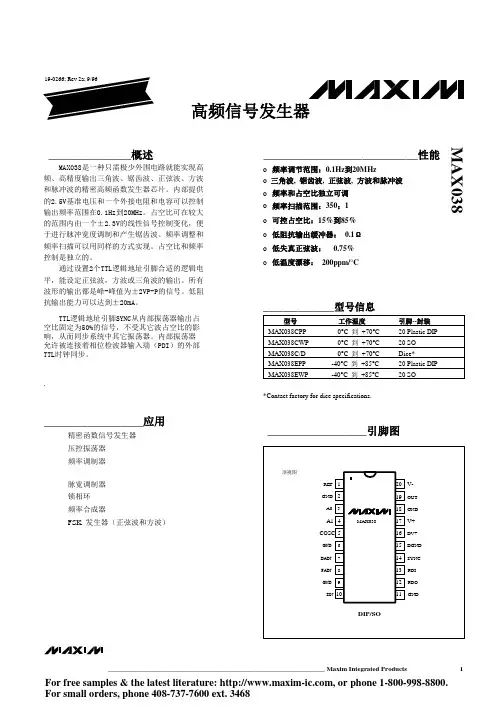
型号 MAX038CPP MAX038CWP MAX038C/D MAX038EPP MAX038EWP工作温度 0°C 到 +70°C 0°C 到 +70°C 0°C 到 +70°C -40°C 到 +85°C -40°C 到 +85°C引脚--封装 20 Plastic DIP 20 SO Dice* 20 Plastic DIP 20 SO.__________________应用精密函数信号发生器 压控振荡器 频率调制器*Contact factory for dice specifications.__________________引脚图脉宽调制器 锁相环 频率合成器FSK 发生器(正弦波和方波)________________________________________________________________ Maxim Integrated Products1For free samples & the latest literature: , or phone 1-800-998-8800. For small orders, phone 408-737-7600 ext. 3468MAX038高频信号发生器图1. 内部结构及基本工作电路_______________ 详细说明MAX038是一种高频函数信号发生器,它可以使 用最少的外部元件而产生低失真正弦波,三角波, 锯齿波,方波(脉冲波)。
MAX4211EEUE+T中文资料
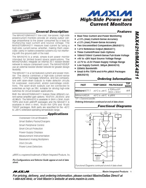
High-Side Power and Current Monitors MAX4210/MAX4211
ABSOLUTE MAXIMUM RATINGS
VCC, IN, CIN1, CIN2 to GND ....................................-0.3V to +6V RS+, RS-, INHIBIT, LE, COUT1, COUT2 to GND ...-0.3V to +30V IOUT, POUT, REF to GND ..........................-0.3V to (VCC + 0.3V) Differential Input Voltage (VRS+ - VRS-) .................................±5V Maximum Current into Any Pin..........................................±10mA Output Short-Circuit Duration to VCC or GND ........................10s Continuous Power Dissipation (TA = +70°C) 6-Pin TDFN (derate 24.4mW/°C above +70°C) ..........1951mW 8-Pin µMAX (derate 4.5mW/°C above +70°C) .............362mW 16-Pin TSSOP (derate 9.4mW/°C above +70°C) ..........754mW 16-Pin Thin QFN (derate 25mW/°C above +70°C) .....2000mW Operating Temperature Range ...........................-40°C to +85°C Junction Temperature ......................................................+150°C Storage Temperature Range .............................-65°C to +150°C Lead Temperature (soldering, 10s) .................................+300°C
MAX3490EESA+中文资料
General DescriptionDevices in the MAX3483E family (MAX3483E/MAX3485E/MAX3486E/MAX3488E/MAX3490E/MAX3491E) are ±15kV ESD-protected, +3.3V, low-power transceivers for RS-485 and RS-422 communications. Each device con-tains one driver and one receiver. The MAX3483E and MAX3488E feature slew-rate-limited drivers that minimize EMI and reduce reflections caused by improperly termi-nated cables, allowing error-free data transmission at data rates up to 250kbps. The partially slew-rate-limited MAX3486E transmits up to 2.5Mbps. The MAX3485E,MAX3490E, and MAX3491E transmit at up to 12Mbps.All devices feature enhanced electrostatic discharge (ESD) protection. All transmitter outputs and receiver inputs are protected to ±15kV using IEC 1000-4-2 Air-Gap Discharge, ±8kV using IEC 1000-4-2 Contact Discharge, and ±15kV using the Human Body Model.Drivers are short-circuit current limited and are protect-ed against excessive power dissipation by thermal shutdown circuitry that places the driver outputs into a high-impedance state. The receiver input has a fail-safe feature that guarantees a logic-high output if both inputs are open circuit.The MAX3488E, MAX3490E, and MAX3491E feature full-duplex communication, while the MAX3483E,MAX3485E, and MAX3486E are designed for half-duplex communication.ApplicationsTelecommunicationsIndustrial-Control Local Area Networks Transceivers for EMI-Sensitive Applications Integrated Services Digital Networks Packet SwitchingFeatureso ESD Protection for RS-485 I/O Pins±15kV—Human Body Model±8kV—IEC 1000-4-2, Contact Discharge ±15kV—IEC 1000-4-2, Air-Gap Discharge o Operate from a Single +3.3V Supply—No Charge Pump Required o Interoperable with +5V Logic o Guaranteed 12Mbps Data Rate (MAX3485E/MAX3490E/MAX3491E)o Slew-Rate Limited for Errorless Data Transmission (MAX3483E/MAX3488E) o 2nA Low-Current Shutdown Mode(MAX3483E/MAX3485E/MAX3486E/MAX3491E)o -7V to +12V Common-Mode Input Voltage Range o Full-Duplex and Half-Duplex Versions Available o Industry-Standard 75176 Pinout (MAX3483E/MAX3485E/MAX3486E)o Current-Limiting and Thermal Shutdown for Driver Overload ProtectionMAX3483E/MAX3485E/MAX3486E/MAX3488E/MAX3490E/MAX3491E3.3V-Powered, ±15kV ESD-Protected, 12Mbps and Slew-Rate-Limited T rue RS-485/RS-422 T ransceivers________________________________________________________________Maxim Integrated Products119-1474; Rev 0; 4/99Selector GuideOrdering InformationOrdering Information continued at end of data sheet.For free samples & the latest literature: , or phone 1-800-998-8800.For small orders, phone 1-800-835-8769.M A X 3483E /M A X 3485E /M A X 3486E /M A X 3488E /M A X 3490E /M A X 3491E3.3V-Powered, ±15kV ESD-Protected, 12Mbps and Slew-Rate-Limited T rue RS-485/RS-422 T ransceiversABSOLUTE MAXIMUM RATINGSDC ELECTRICAL CHARACTERISTICS(V = +3.3V ±0.3V, T = T to T , unless otherwise noted. Typical values are at T = +25°C.)Stresses beyond those listed under “Absolute Maximum Ratings” may cause permanent damage to the device. These are stress ratings only, and functional operation of the device at these or any other conditions beyond those indicated in the operational sections of the specifications is not implied. Exposure to absolute maximum rating conditions for extended periods may affect device reliability.Supply Voltage (V CC ).............................................................+7V Control Input Voltage (RE , DE).................................-0.3V to +7V Driver Input Voltage (DI)...........................................-0.3V to +7V Driver Output Voltage (A, B, Y, Z).......................-7.5V to +12.5V Receiver Input Voltage (A, B)..............................-7.5V to +12.5V Receiver Output Voltage (RO)....................-0.3V to (V CC + 0.3V)Continuous Power Dissipation (T A = +70°C)8-Pin SO (derate 5.88mW/°C above +70°C)..................471mW 8-Pin Plastic DIP (derate 9.09mW/°C above +70°C).....727mW14-Pin SO (derate 8.33mW/°C above +70°C)................667mW 14-Pin Plastic DIP (derate 10mW/°C above +70°C)......800mW Operating Temperature RangesMAX34_ _ EC_ _...................................................0°C to +70°C MAX34_ _ EE_ _.................................................-40°C to +85°C Storage Temperature Range.............................-65°C to +150°C Lead Temperature (soldering, 10sec).............................+300°CMAX3483E/MAX3485E/MAX3486E/MAX3488E/MAX3490E/MAX3491E3.3V-Powered, ±15kV ESD-Protected, 12Mbps and Slew-Rate-Limited T rue RS-485/RS-422 T ransceiversDC ELECTRICAL CHARACTERISTICS (continued)(V CC = +3.3V ±0.3V, T A = T MIN to T MAX , unless otherwise noted. Typical values are at T A = +25°C.)DRIVER SWITCHING CHARACTERISTICS—MAX3485E/MAX3490E/MAX3491E(V = +3.3V, T = +25°C.)DRIVER SWITCHING CHARACTERISTICS—MAX3486E(V = +3.3V, T = +25°C.)*MAX3488E and MAX3491E will be compliant to ±8kV per IEC 1000-4-2 Contact Discharge by September 1999.M A X 3483E /M A X 3485E /M A X 3486E /M A X 3488E /M A X 3490E /M A X 3491E3.3V-Powered, ±15kV ESD-Protected, 12Mbps and Slew-Rate-Limited T rue RS-485/RS-422 T ransceivers4_______________________________________________________________________________________DRIVER SWITCHING CHARACTERISTICS—MAX3483E/MAX3488E(V CC = +3.3V, T A = +25°C.)RECEIVER SWITCHING CHARACTERISTICS(V CC = +3.3V, T A = +25°C.)Note 1:∆V OD and ∆V OC are the changes in V OD and V OC , respectively, when the DI input changes state.Note 2:Measured on |t PLH (Y) - t PHL (Y)|and |t PLH (Z) - t PHL (Z)|.Note 3:The transceivers are put into shutdown by bringing RE high and DE low. If the inputs are in this state for less than 80ns, thedevices are guaranteed not to enter shutdown. If the inputs are in this state for at least 300ns, the devices are guaranteed to have entered shutdown. See Low-Power Shutdown Mode section.MAX3483E/MAX3485E/MAX3486E/MAX3488E/MAX3490E/MAX3491E3.3V-Powered, ±15kV ESD-Protected, 12Mbps and Slew-Rate-Limited T rue RS-485/RS-422 T ransceivers_______________________________________________________________________________________5Typical Operating Characteristics(V CC = +3.3V, T A = +25°C, unless otherwise noted.)252015105000.51.01.52.02.53.53.0OUTPUT CURRENT vs.RECEIVER OUTPUT LOW VOLTAGEM A X 3483E -01OUTPUT LOW VOLTAGE (V)O U T P U T C U R R E N T (m A )-20-18-16-14-12-10-8-6-4-2000.51.01.52.02.53.53.0OUTPUT CURRENT vs.RECEIVER OUTPUT HIGH VOLTAGEM A X 3483E -02OUTPUT HIGH VOLTAGE (V)O U T P U T C U R R E N T (m A )3.003.053.103.153.203.253.30-40-20020406010080RECEIVER OUTPUT HIGH VOLTAGEvs. TEMPERATURETEMPERATURE (°C)O U T P U T H I G H V O L T A G E (V )00.10.20.30.40.50.60.70.8-40-2020406010080RECEIVER OUTPUT LOW VOLTAGEvs. TEMPERATURETEMPERATURE (°C)O U T P U T L O W V O L T A G E (V )2505075100125150175024681012OUTPUT CURRENT vs.DRIVER OUTPUT LOW VOLTAGEM A X 3483E -07OUTPUT LOW VOLTAGE (V)O U T P U T C U R R E N T (m A )100908070605040302010000.5 1.0 1.5 2.0 2.5 3.53.0DRIVER OUTPUT CURRENT vs.DIFFERENTIAL OUTPUT VOLTAGEM A X 3483E -05DIFFERENTIAL OUTPUT VOLTAGE (V)O U T P U T C U R R E N T (m A )1.61.71.81.92.02.12.22.32.42.62.5-40-20020406010080DRIVER DIFFERENTIAL OUTPUT VOLTAGE vs. TEMPERATURETEMPERATURE (°C)D I F FE R E N T I A L O U T P U T V O L T A G E (V )-100-80-60-40-20543210-7-6-3-4-5-2-1OUTPUT CURRENT vs.DRIVER OUTPUT HIGH VOLTAGEM A X 3483E -08OUTPUT HIGH VOLTAGE (V)O U T P U T C U R R E N T (m A )M A X 3483E /M A X 3485E /M A X 3486E /M A X 3488E /M A X 3490E /M A X 3491E3.3V-Powered, ±15kV ESD-Protected, 12Mbps and Slew-Rate-Limited T rue RS-485/RS-422 T ransceivers0.80.70.91.01.11.2-40-2020406010080SUPPLY CURRENT vs. TEMPERATURETEMPERATURE (°C)S U P P L Y C U R R E N T (m A )Typical Operating Characteristics (continued)(V CC = +3.3V, T A = +25°C, unless otherwise noted.)0102030405060708010090-40-2020406010080SHUTDOWN CURRENT vs. TEMPERATUREM A X 3483E -10TEMPERATURE (°C)S H U T D O W N C U R R E N T (n A )Pin DescriptionMAX3483E/MAX3485E/MAX3486E/MAX3488E/MAX3490E/MAX3491E3.3V-Powered, ±15kV ESD-Protected, 12Mbps and Slew-Rate-Limited T rue RS-485/RS-422 T ransceivers_______________________________________________________________________________________7Figure 2. MAX3488E/MAX3490E Pin Configuration and Typical Operating CircuitFigure 3. MAX3491E Pin Configuration and Typical Operating CircuitFigure 1. MAX3483E/MAX3485E/MAX3486E Pin Configuration and Typical Operating CircuitM A X 3483E /M A X 3485E /M A X 3486E /M A X 3488E /M A X 3490E /M A X 3491E3.3V-Powered, ±15kV ESD-Protected, 12Mbps and Slew-Rate-Limited T rue RS-485/RS-422 T ransceivers8_______________________________________________________________________________________Figure 4. Driver V OD and V OC Figure 7. Driver Differential Output Delay and Transition TimesFigure 6. Receiver V OH and V OLFigure 5. Driver V OD with Varying Common-Mode VoltageMAX3483E/MAX3485E/MAX3486E/MAX3488E/MAX3490E/MAX3491E3.3V-Powered, ±15kV ESD-Protected, 12Mbps and Slew-Rate-Limited T rue RS-485/RS-422 T ransceivers_______________________________________________________________________________________9Figure 8. Driver Propagation TimesFigure 9. Driver Enable and Disable Times (t PZH , t PSH , t PHZ )Figure 10. Driver Enable and Disable Times (t PZL , t PSL , t PLZ )M A X 3483E /M A X 3485E /M A X 3486E /M A X 3488E /M A X 3490E /M A X 3491E3.3V-Powered, ±15kV ESD-Protected, 12Mbps and Slew-Rate-Limited T rue RS-485/RS-422 T ransceivers10______________________________________________________________________________________Figure 11. Receiver Propagation DelayFigure 12. Receiver Enable and Disable TimesNote 4: The input pulse is supplied by a generator with the following characteristics: f = 250kHz, 50% duty cycle, t r ≤6.0ns, Z O = 50Ω.Note 5: C L includes probe and stray capacitance._____________________Function TablesDevices with Receiver/Driver Enable(MAX3483E/MAX3485E/MAX3486E/MAX3491E)Table 1. Transmitting* B and A outputs are Z and Y, respectively, for full-duplex part (MAX3491E).X = Don’t care; High-Z = High impedanceTable 2. Receiving* DE is a “don’t care” (x) for the full-duplex part (MAX3491E).X = Don’t care; High-Z = High impedanceDevices without Receiver/Driver Enable(MAX3488E/MAX3490E)Table 3. TransmittingTable 4. Receiving___________Applications InformationThe MAX3483E/MAX3485E/MAX3486E/MAX3488E/MAX3490E/MAX3491E are low-power transceivers for RS-485 and RS-422 communications. The MAX3483E and MAX3488E can transmit and receive at data rates up to 250kbps, the MAX3486E at up to 2.5Mbps, and the MAX3485E/MAX3490E/MAX3491E at up to 12Mbps. The MAX3488E/MAX3490E/MAX3491E are full-duplex trans-ceivers, while the MAX3483E/MAX3485E/MAX3486E are half-duplex. Driver Enable (DE) and Receiver Enable (RE ) pins are included on the MAX3483E/MAX3485E/MAX3486E/MAX3491E. When disabled, the driver and receiver outputs are high impedance.Reduced EMI and Reflections (MAX3483E/MAX3486E/MAX3488E)The MAX3483E/MAX3488E are slew-rate limited, mini-mizing EMI and reducing reflections caused by improp-erly terminated cables. Figure 13 shows the driver output waveform of a MAX3485E/MAX3490E/MAX3491E transmitting a 125kHz signal, as well as the Fourier analysis of that waveform. High-frequency harmonics with large amplitudes are evident. Figure 14 shows the same information, but for the slew-rate-limited MAX3483E/MAX3488E transmitting the same signal. The high-frequency harmonics have much lower amplitudes,and the potential for EMI is significantly reduced.Low-Power Shutdown Mode(MAX3483E/MAX3485E/MAX3486E/MAX3491E)A low-power shutdown mode is initiated by bringing both RE high and DE low. The devices will not shut down unless both the driver and receiver are disabled (high impedance). In shutdown, the devices typically draw only 2nA of supply current.For these devices, the t PSH and t PSL enable times assume the part was in the low-power shutdown mode;the t PZH and t PZL enable times assume the receiver or driver was disabled, but the part was not shut down.MAX3483E/MAX3485E/MAX3486E/MAX3488E/MAX3490E/MAX3491E3.3V-Powered, ±15kV ESD-Protected, 12Mbps and Slew-Rate-Limited T rue RS-485/RS-422 T ransceivers______________________________________________________________________________________11INPUTS OUTPUT A, B RO ≥+0.2V 1≤-0.2V 0Inputs Open1INPUT OUTPUTS DI Z Y 101015MHz 500kHz/div 05MHz500kHz/div Figure 13. Driver Output Waveform and FFT Plot of MAX3485E/MAX3490E/MAX3491E Transmitting a 125kHz Signal Figure 14. Driver Output Waveform and FFT Plot of MAX3483E/ MAX3488E Transmitting a 125kHz SignalM A X 3483E /M A X 3485E /M A X 3486E /M A X 3488E /M A X 3490E /M A X 3491E3.3V-Powered, ±15kV ESD-Protected, 12Mbps and Slew-Rate-Limited T rue RS-485/RS-422 T ransceivers12______________________________________________________________________________________Figure 17. MAX3483E/MAX3488E Driver Propagation Delay Figure 19. MAX3483E/MAX3488E System Differential Voltage at 125kHz Driving 4000 Feet of Cable Figure 20. MAX3485E/MAX3490E/MAX3491E System Differential Voltage at 125kHz Driving 4000 Feet of CableDriver-Output Protection Excessive output current and power dissipation caused by faults or by bus contention are prevented by two mechanisms. A foldback current limit on the output stage provides immediate protection against short circuits over the whole common-mode voltage range (see Typical Operating Characteristics). In addition, a thermal shut-down circuit forces the driver outputs into a high-imped-ance state if the die temperature rises excessively.Propagation Delay Figures 15–18 show the typical propagation delays. Skew time is simply the difference between the low-to-high and high-to-low propagation delay. Small driver/receiver skew times help maintain a symmetrical mark-space ratio (50% duty cycle).The receiver skew time, |t PRLH- t PRHL|, is under 10ns (20ns for the MAX3483E/MAX3488E). The driver skew times are 8ns for the MAX3485E/MAX3490E/MAX3491E, 12ns for the MAX3486E, and typically under 50ns for the MAX3483E/MAX3488E.Line Length vs. Data Rate The RS-485/RS-422 standard covers line lengths up to 4000 feet. For line lengths greater than 4000 feet, see Figure 21 for an example of a line repeater.Figures 19 and 20 show the system differential voltage for parts driving 4000 feet of 26AWG twisted-pair wire at 125kHz into 120Ωloads.For faster data rate transmission, please consult the fac-tory.±15kV ESD Protection As with all Maxim devices, ESD-protection structures are incorporated on all pins to protect against electrostatic discharges encountered during handling and assembly. The driver outputs and receiver inputs of the MAX3483E family of devices have extra protection against static electricity. Maxim’s engineers have developed state-of-the-art structures to protect these pins against ESD of ±15kV without damage. The ESD structures withstand high ESD in all states: normal operation, shutdown, and powered down. After an ESD event, Maxim’s E versions keep working without latchup or damage.ESD protection can be tested in various ways; the transmitter outputs and receiver inputs of this product family are characterized for protection to the following limits:1)±15kV using the Human Body Model2)±8kV using the Contact-Discharge method specifiedin IEC 1000-4-23)±15kV using IEC 1000-4-2’s Air-Gap method.ESD Test Conditions ESD performance depends on a variety of conditions. Contact Maxim for a reliability report that documents test setup, test methodology, and test results.Human Body Model Figure 22a shows the Human Body Model and Figure 22b shows the current waveform it generates when dis-charged into a low impedance. This model consists of a 100pF capacitor charged to the ESD voltage of inter-est, which is then discharged into the test device through a 1.5kΩresistor.IEC 1000-4-2 The IEC 1000-4-2 standard covers ESD testing and performance of finished equipment; it does not specifi-cally refer to integrated circuits. The MAX3483E family of devices helps you design equipment that meets Level 4 (the highest level) of IEC 1000-4-2, without the need for additional ESD-protection components.The major difference between tests done using the Human Body Model and IEC 1000-4-2 is higher peak current in IEC 1000-4-2, because series resistance is lower in the IEC 1000-4-2 model. Hence, the ESD with-stand voltage measured to IEC 1000-4-2 is generally lower than that measured using the Human Body Model. Figure 23a shows the IEC 1000-4-2 model, and Figure 23b shows the current waveform for the ±8kV IEC 1000-4-2, Level 4 ESD contact-discharge test.Figure 21. Line Repeater for MAX3488E/MAX3490E/MAX3491EMAX3483E/MAX3485E/MAX3486E/MAX3488E/MAX3490E/MAX3491E3.3V-Powered, ±15kV ESD-Protected, 12Mbps and Slew-Rate-Limited T rue RS-485/RS-422 T ransceivers ______________________________________________________________________________________13M A X 3483E /M A X 3485E /M A X 3486E /M A X 3488E /M A X 3490E /M A X 3491EThe air-gap test involves approaching the device with a charged probe. The contact-discharge method connects the probe to the device before the probe is energized.Machine ModelThe Machine Model for ESD tests all pins using a 200pF storage capacitor and zero discharge resis-tance. Its objective is to emulate the stress caused when I/O pins are contacted by handling equipment during test and assembly. Of course, all pins require this protection, not just RS-485 inputs and outputs.Typical ApplicationsThe MAX3483E/MAX3485E/MAX3486E/MAX3488E/MAX3490E/MAX3491E transceivers are designed for bidirectional data communications on multipoint bus transmission lines. Figures 24 and 25 show typical net-work applications circuits. These parts can also be used as line repeaters, with cable lengths longer than 4000 feet, as shown in Figure 21.To minimize reflections, the line should be terminated at both ends in its characteristic impedance, and stub lengths off the main line should be kept as short as possible. The slew-rate-limited MAX3483E/MAX3488E and the partially slew-rate-limited MAX3486E are more tolerant of imperfect termination.3.3V-Powered, ±15kV ESD-Protected, 12Mbps and Slew-Rate-Limited T rue RS-485/RS-422 T ransceivers14______________________________________________________________________________________Figure 22a. Human Body ESD Test ModelFigure 22b. Human Body Current WaveformFigure 23a. IEC 1000-4-2 ESD Test ModelFigure 23b. IEC 1000-4-2 ESD Generator Current WaveformMAX3483E/MAX3485E/MAX3486E/MAX3488E/MAX3490E/MAX3491E3.3V-Powered, ±15kV ESD-Protected, 12Mbps and Slew-Rate-Limited T rue RS-485/RS-422 T ransceivers______________________________________________________________________________________15Figure 25. MAX3488E/MAX3490E/MAX3491E Full-Duplex RS-485 NetworkFigure 24. MAX3483E/MAX3485E/MAX3486E Typical RS-485 NetworkM A X 3483E /M A X 3485E /M A X 3486E /M A X 3488E /M A X 3490E /M A X 3491E3.3V-Powered, ±15kV ESD-Protected, 12Mbps and Slew-Rate-Limited T rue RS-485/RS-422 T ransceiversTRANSISTOR COUNT: 761Chip InformationOrdering Information (continued)Maxim cannot assume responsibility for use of any circuitry other than circuitry entirely embodied in a Maxim product. No circuit patent licenses are implied. Maxim reserves the right to change the circuitry and specifications without notice at any time.16____________________Maxim Integrated Products, 120 San Gabriel Drive, Sunnyvale, CA 94086 408-737-7600©1999 Maxim Integrated ProductsPrinted USAis a registered trademark of Maxim Integrated Products.。
MAX338ESE+中文资料
MAX338EPE -40°C to +85°C 16 Plastic DIP
MAX338ESE -40°C to +85°C 16 Narrow SO
MAX338EJE -40°C to +85°C 16 CERDIP
MAX338MJE -55°C to +125°C 16 CERDIP**
Ordering Information continued at end of data sheet. *Contact factory for dice specifications. **Contact factory for availability.
元器件交易网
19-0272; Rev 3; 11/04
MAX338/MAX3ห้องสมุดไป่ตู้9
8-Channel/Dual 4-Channel, Low-Leakage, CMOS Analog Multiplexers
General Description
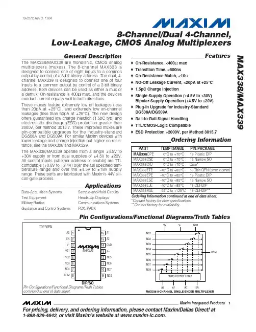
The MAX338/MAX339 are monolithic, CMOS analog multiplexers (muxes). The 8-channel MAX338 is designed to connect one of eight inputs to a common output by control of a 3-bit binary address. The dual, 4channel MAX339 is designed to connect one of four inputs to a common output by control of a 2-bit binary address. Both devices can be used as either a mux or a demux. On-resistance is 400Ω max, and the devices conduct current equally well in both directions.
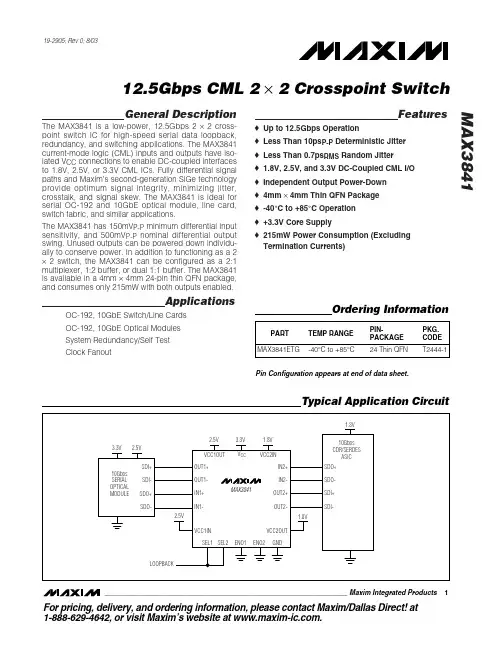
MAX3841中文资料
PARAMETER
SYMBOL
CONDITIONS
MIN TYP MAX UNITS
Core Supply Current Data Rate
ICC
Excluding CML termination currents
(Note 1)
65
90
mA
0
12.5 Gbps
CML Input Differential CML Input Common Mode
Termination Currents)
Ordering Information
PART
TEMP RANGE
MAX3841ETG -40°C to +85°C
PINPACKAGE
24 Thin QFN
PKG. CODE
T2444-1
Pin Configuration appears at end of data sheet.
12
dB
CML Output Differential CML Output Termination
VOUT
(Note 2) Single ended
400
500
42.5
50
600 57.5
mVP-P Ω
CML Output Transition Time Deterministic Jitter Random Jitter Propagation Delay
Note 4: Measured at 9.953Gbps using a pattern of 100 ones, 27 - 1 PRBS, 100 zeros, 27 - 1 PRBS, and at 12.5Gbps using a ±K28.5 pattern. VCC_IN = VCC_OUT = 1.8V, and VIN = 400mVP-P differential.
MAX3232EEAE中文资料
MAX3222EEPN -40°C to +85°C 18 Plastic DIP —
MAX3232ECAE 0°C to +70°C 16 SSOP
—
MAX3232ECWE 0°C to +70°C 16 Wide SO —
MAX3232ECPE 0°C to +70°C 16 Plastic DIP —
General Description
The MAX3222E/MAX3232E/MAX3237E/MAX3241E/ MAX3246E +3.0V-powered EIA/TIA-232 and V.28/V.24 communications interface devices feature low power consumption, high data-rate capabilities, and enhanced electrostatic-discharge (ESD) protection. The enhanced ESD structure protects all transmitter outputs and receiver inputs to ±15kV using IEC 1000-4-2 Air-Gap Discharge, ±8kV using IEC 1000-4-2 Contact Discharge (±9kV for MAX3246E), and ±15kV using the Human Body Model. The logic and receiver I/O pins of the MAX3237E are protected to the above standards, while the transmitter output pins are protected to ±15kV using the Human Body Model.
33811资料
12 11 10 9
Figure 3. 33811 Pin Connections Table 1. 33811 Pin Definitions A functional description of each pin can be found in the Functional Pin Description section beginning on page 11.
元器件交易网
PIN CONNECTIONS
PIN CONNECTIONS
VDD D_GND SO SI CS SCLK RESET VSPI 1 2 3 4 5 6 7 8 16 15 14
13
A_GND N/C SOLM1 SOLM2 SOLM3 SOLM4 SOLM5 VPWR
33811
SOLENOID MONITOR
EG SUFFIX (PB_FREE) 98ASB42567B 16-PIN SOICW
ORDERING INFORMATION
Device PCZ33811EG/R2 Temperature Range (TA) -40°C to 125°C Package 16 SOICW
© Freescale Semiconductor, Inc., 2007. All rights reserved.
元器件交易网
INTERNAL BLOCK DIAGRAM
INTERNAL BLOCK DIAGRAM
VPWR VDD
VPWR, VDD, 5.0 V Oscillator and Clock Generator
Pin Number 1 2 3 Pin Name VDD D_GND SO Pin Function Power Ground Output Formal Name Digital Voltage Supply Digital Ground Serial Output Data Definition The VDD pin is the digital logic supply voltage used internally in the IC. Digital ground for the internal control circuits of the IC. This ground should be used for decoupling of the VDD supply. The SO output pin is used to transmit serial data from the device to the MCU. The SO pin remains tri-state until selected by the active low CS. The serial output data is available to be latched by the MCU on the rising edge of SCLK. The SO data transitions on falling edge of the SCLK. The SI input pin is used to receive serial data from the MCU. The serial input data is latched on the rising edge of SCLK, and the input data transitions on the falling edge of SCLK. The Chip Select input pin is an active low signal sent by the MCU to indicate that the device is being addressed. This input requires CMOS logic levels and has an internal active pull-up current source. The SCLK input pin is used to clock in and out the serial data on the SI and SO pins while being addressed by the CS. The SCLK signal consists of a 50% duty cycle with CMOS logic levels. Input data is latched by the device on the rising edge of SCLK while output data is changed on the falling edge. SCLK is ignored by the device while CS is high. The RESET pin, when pulled high, clears any fault bits and causes the Serial Output pin to be tri-stated. The RESET pin operates at the CMOS levels dictated by the VDD line and the state of the VSPI pin. The VSPI pin determines the voltage levels for the SPI interface. It must be connected to the same voltage supply (+5 volts or +3.3 Volts) as the MCU’s SPI interface.
MAX3087ESA中文资料
375
256
MAX3084
Full
0.5
Yes
No
No
375
256
MAX3085
Half
0.5
Yes
Yes
Yes
375
256
MAX3086
Full
10
No
Yes
Yes
375
256
MAX3087
Full
10
No
No
No
375
256
MAX3088
Half
10
No
Yes
Yes
375
256
MAX3089 Selectable Selectable Selectable
These transceivers typically draw 375µA of supply current when unloaded, or when fully loaded with the drivers disabled.
All devices have a 1/8-unit-load receiver input impedance that allows up to 256 transceivers on the bus. The MAX3082/MAX3085/MAX3088 are intended for halfduplex communications, while the MAX3080/MAX3081/ MAX3083/MAX3084/MAX3086/MAX3087 are intended for full-duplex communications. The MAX3089 is selectable between half-duplex and full-duplex operation. It also features independently programmable receiver and transmitter output phase via separate pins.
MAX3491ECSD中文资料
MAX3483E/MAX3485E/MAX3486E/MAX3488E/MAX3490E/MAX3491E
19-1474; Rev 0; 4/99
3.3V-Powered, ±15kV ESD-Protected, 12Mbps and Slew-Rate-Limited True RS-485/RS-422 Transceivers
PART
TEMP. RANGE PIN-PACKAGE
MAX3483ECSA
0°C to +70°C
8 SO
MAX3483ECPA
0°C to +70°C
8 Plastic DIP
MAX3483EESA -40°C to +85°C
8 SO
MAX3483EEPA -40°C to +85°C
8 Plastic DIP
o Industry-Standard 75176 Pinout (MAX3483E/MAX3485E/MAX3486E)
o Current-Limiting and Thermal Shutdown for Driver Overload Protection
Ordering Information
General Description
Devices in the MAX3483E family (MAX3483E/MAX3485E/ MAX3486E/MAX3488E/MAX3490E/MAX3491E) are ±15kV ESD-protected, +3.3V, low-power transceivers for RS-485 and RS-422 communications. Each device contains one driver and one receiver. The MAX3483E and MAX3488E feature slew-rate-limited drivers that minimize EMI and reduce reflections caused by improperly terminated cables, allowing error-free data transmission at data rates up to 250kbps. The partially slew-rate-limited MAX3486E transmits up to 2.5Mbps. The MAX3485E, MAX3490E, and MAX3491E transmit at up to 12Mbps.
MAX3313EEUB-T中文资料
General DescriptionThe MAX3311E/MAX3313E are low-power, 5V EIA/TIA-232-compatible transceivers. All transmitter outputs and receiver inputs are protected to ±15kV using the Human Body Model, making these devices ideal for applications where more robust transceivers are required.Both devices have one transmitter and one receiver.The transmitters have a proprietary low-dropout trans-mitter output stage enabling RS-232-compatible opera-tion from a +5V supply with a single inverting charge pump. These transceivers require only three 0.1µF capacitors and will run at data rates up to 460kbps while maintaining RS-232-compatible output levels.The MAX3311E features a 1µA shutdown mode. In shutdown the device turns off the charge pump, pulls V- to ground, and the transmitter output is disabled.The MAX3313E features an INVALID output that asserts high when an active RS-232 cable signal is connected,signaling to the host that a peripheral is connected to the communication port.________________________ApplicationsDigital Cameras PDAs GPS POSTelecommunications Handy Terminals Set-Top BoxesFeatureso ESD Protection for RS-232-Compatible I/O Pins±15kV—Human Body Modelo 1µA Low-Power Shutdown (MAX3311E)o INVALID Output (MAX3313E)o Receiver Active in Shutdown (MAX3311E)o Single Transceiver (1Tx/1Rx) in 10-Pin µMAX PackageMAX3311E/MAX3313E±15kV ESD-Protected, 460kbps, 1µA,RS-232-Compatible Transceivers in µMAX________________________________________________________________Maxim Integrated Products1Pin Configurations19-1910; Rev 0; 1/01Ordering InformationFor price, delivery, and to place orders,please contact Maxim Distribution at 1-888-629-4642,or visit Maxim’s website at .Typical Operating CircuitM A X 3311E /M A X 3313E±15kV ESD-Protected, 460kbps, 1µA,RS-232-Compatible Transceivers in µMAX 2_______________________________________________________________________________________ABSOLUTE MAXIMUM RATINGSELECTRICAL CHARACTERISTICSStresses beyond those listed under “Absolute Maximum Ratings” may cause permanent damage to the device. These are stress ratings only, and functional operation of the device at these or any other conditions beyond those indicated in the operational sections of the specifications is not implied. Exposure to absolute maximum rating conditions for extended periods may affect device reliability.V CC to GND.............................................................-0.3V to +6V V- to GND................................................................+0.3V to -7V V CC + |V-|............................................................................+13V Input VoltagesTIN, SHDN to GND...............................................-0.3V to +6V RIN to GND......................................................................±25V Output VoltagesTOUT to GND................................................................±13.2V ROUT, INVALID to GND.....................…-0.3V to (V CC + 0.3V)Short-Circuit DurationTOUT to GND.........................................................ContinuousContinuous Power Dissipation10-Pin µMAX (derate 5.6mW/°C above +70°C)..........444mW Operating Temperature RangesMAX331_ECUB.................................................0°C to +70°C MAX331_EEUB..............................................-40°C to +85°C Junction Temperature.....................................................+150°C Storage Temperature Range............................-65°C to +150°C Lead Temperature (soldering, 10s)................................+300°CMAX3311E/MAX3313E±15kV ESD-Protected, 460kbps, 1µA,RS-232-Compatible Transceivers in µMAX_______________________________________________________________________________________3ELECTRICAL CHARACTERISTICS (continued)TIMING CHARACTERISTICSM A X 3311E /M A X 3313E±15kV ESD-Protected, 460kbps, 1µA,RS-232-Compatible Transceivers in µMAX 4_______________________________________________________________________________________Typical Operating Characteristics(V CC = +5V, 0.1µF capacitors, transmitter loaded with 3k Ωand C L , T A = +25°C, unless otherwise noted.)0428612101410001500500200025003000SLEW RATEvs. LOAD CAPACITANCELOAD CAPACITANCE (pF)S L E W R A T E (V /µs )-5-4-3-2-10123456050010001500200025003000TRANSMITTER OUTPUT VOLTAGEvs. LOAD CAPACITANCELOAD CAPACITANCE (pF)T R A N S M I T T E R O U T P U T V O L T A G E (V )010001500500200025003000SUPPLY CURRENT vs. LOAD CAPACITANCELOAD CAPACITANCE (pF)Detailed DescriptionSingle Charge-Pump Voltage ConverterThe MAX3311E/MAX3313E internal power supply has a single inverting charge pump that provides a negative voltage from a single +5V supply. The charge pump operates in a discontinuous mode and requires a flying capacitor (C1) and a reservoir capacitor (C2) to gener-ate the V- supply.RS-232-Compatible DriverThe transmitter is an inverting level translator that con-verts CMOS-logic levels to EIA/TIA-232 compatible lev-els. It guarantees data rates up to 460kbps with worst-case loads of 3k Ωin parallel with 1000pF. When SHDN is driven low, the transmitter is disabled and put into tri-state. The transmitter input does not have an internal pullup resistor.RS-232 ReceiverThe MAX3311E/MAX3313E receiver converts RS-232signals to CMOS-logic output levels. The MAX3311E receiver will remain active during shutdown mode. The MAX3313E INVALID indicates when an RS-232 signal is present at the receiver input, and therefore when the port is in use.The MAX3313E INVALID output is pulled low when no valid RS-232 signal level is detected on the receiver input.MAX3311E Shutdown ModeIn shutdown mode, the charge pump is turned off, V- is pulled to ground, and the transmitter output is disabled (Table 1). This reduces supply current typically to 1µA.The time required to exit shutdown is less than 25ms.Applications InformationCapacitor SelectionThe capacitor type used for C1 and C2 is not critical for proper operation; either polarized or nonpolarized capacitors are acceptable. If polarized capacitors are used, connect polarity as shown in the Typical Operating Circuit . The charge pump requires 0.1µF capacitors. Increasing the capacitor values (e.g., by a factor of 2) reduces power consumption. C2 can beincreased without changing C1’s value. However, do not increase C1’s value without also increasing the value of C2 and C BYPASS to maintain the proper ratios (C1 to the other capacitors).When using the minimum 0.1µF capacitors, make sure the capacitance does not degrade excessively with temperature. If in doubt, use capacitors with a larger nominal value. The capacitor ’s equivalent series resis-tance (ESR) usually rises at low temperatures and influ-ences the amount of ripple on V-.To reduce the output impedance at V-, use larger capacitors (up to 10µF).Bypass V CC to ground with at least 0.1µF. In applica-tions sensitive to power-supply noise generated by the charge pump, decouple V CC to ground with a capaci-tor the same size as (or larger than) charge-pump capacitors C1 and C2.Transmitter Output when ExitingShutdownFigure 1 shows the transmitter output when exiting shutdown mode. The transmitter is loaded with 3k Ωin parallel with 1000pF. The transmitter output displays no ringing or undesirable transients as the MAX3311E comes out of shutdown. Note that the transmitter is enabled only when the magnitude of V- exceeds approximately -3V.High Data RatesThe MAX3311E/MAX3313E maintain RS-232-compati-ble ±3.7V minimum transmitter output voltage even atMAX3311E/MAX3313E±15kV ESD-Protected, 460kbps, 1µA,RS-232-Compatible Transceivers in µMAX5Figure 1. Transmitter Output when Exiting Shutdown or Powering Up10µs/divSHDNTOUT5V/div1.5V/divTIN = GNDTIN = V CCM A X 3311E /M A X 3313E±15kV ESD-Protected, 460kbps, 1µA,RS-232-Compatible Transceivers in µMAX 6_______________________________________________________________________________________high data rates. Figure 2 shows a transmitter loopback test circuit. Figure 3 shows the loopback test result at 120kbps, and Figure 4 shows the same test at 250kbps.±15kV ESD ProtectionAs with all Maxim devices, ESD-protection structures are incorporated on all pins to protect against electro-static discharges encountered during handling and assembly. The MAX3311E/MAX3313E driver outputsand receiver inputs have extra protection against static discharge. Maxim ’s engineers have developed state-of-the-art structures to protect these pins against ESD of ±15kV without damage. The ESD structures withstand high ESD in all states: normal operation, shutdown, and powered down. After an ESD event, Maxim ’s E versions keep working without latchup; whereas, competing products can latch and must be powered down to remove latchup.ESD protection can be tested in various ways. The transmitter outputs and receiver inputs of the product family are characterized for protection to ±15kV using the Human Body Model.ESD Test ConditionsESD performance depends on a variety of conditions.Contact Maxim for a reliability report that documents test setup, test methodology, and test results.Human Body ModelFigure 5 shows the Human Body Model, and Figure 6shows the current waveform it generates when dis-charged into low impedance. This model consists of a 100pF capacitor charged to the ESD voltage of interest,which is then discharged into the test device through a 1.5k Ωresistor.Machine ModelThe Machine Model for ESD tests all pins using a 200pF storage capacitor and zero discharge resis-tance. Its objective is to emulate the stress caused by contact that occurs with handling and assembly during manufacturing. Of course, all pins require this protec-tion during manufacturing, not just RS-232 inputs and outputs. Therefore, after PC board assembly, the Machine Model is less relevant to I/O ports.Figure 4. Loopback Test Results at 250kbps2µs/divTOUTTINROUTFigure 3. Loopback Test Results at 120kbps 5µs/divTOUTTINROUTMAX3311E/MAX3313E±15kV ESD-Protected, 460kbps, 1µA,RS-232-Compatible Transceivers in µMAX_______________________________________________________________________________________7Figure 5. Human Body ESD Test ModelFigure 6. Human Body Current WaveformPin Configurations (continued)Chip InformationTRANSISTOR COUNT: 278M A X 3311E /M A X 3313E±15kV ESD-Protected, 460kbps, 1µA,RS-232-Compatible Transceivers in µMAX Maxim cannot assume responsibility for use of any circuitry other than circuitry entirely embodied in a Maxim product. No circuit patent licenses are implied. Maxim reserves the right to change the circuitry and specifications without notice at any time.8_____________________Maxim Integrated Products, 120 San Gabriel Drive, Sunnyvale, CA 94086 408-737-7600©2001 Maxim Integrated ProductsPrinted USAis a registered trademark of Maxim Integrated Products.______________________________________________________________Pin Description。
- 1、下载文档前请自行甄别文档内容的完整性,平台不提供额外的编辑、内容补充、找答案等附加服务。
- 2、"仅部分预览"的文档,不可在线预览部分如存在完整性等问题,可反馈申请退款(可完整预览的文档不适用该条件!)。
- 3、如文档侵犯您的权益,请联系客服反馈,我们会尽快为您处理(人工客服工作时间:9:00-18:30)。
General DescriptionThe MAX3380E/MAX3381E are +2.35V to +5.5V-pow-ered EI A/TI A-232 and V.28/V.24 communication inter-faces with low power requirements, high data-rate capabilities, and enhanced electrostatic discharge (ESD) protection on both the TTL and RS-232 sides.The MAX3380E/MAX3381E have two receivers and two transmitters. All RS-232 inputs, outputs, and logic input pins are protected to ±15kV using I EC 1000-4-2 Air-Gap Discharge method and the Human Body Model,and ±8kV using I EC 1000-4-2 Contact Discharge method.The proprietary low-dropout transmitter output stage enables true RS-232 performance from a +3.1V to +5.5V supply with a dual charge pump. The parts reduce the transmitter output levels to RS-232-compati-ble levels with no increase in supply current for sup-plies less than +3.1V and greater than +2.35V. The +2.35V to +5.5V operating range is fully compatible with lithium-ion (Li+) batteries. The charge pump requires only four small 0.1µF capacitors for operation. The MAX3380E/MAX3381E transceivers use Maxim’s revolutionary AutoShutdown Plus™ feature to auto-matically enter a 1µA shutdown mode. These devices shut down the on-board power supply and drivers when they do not sense a valid signal transi-tion for 30 seconds on either the receiver or trans-mitter inputs.The MAX3380E is capable of transmitting data at rates of 460kbps while maintaining RS-232 output levels, and the MAX3381E operates at data rates up to 250kbps. The MAX3381E offers a slower slew rate for applications where noise and EMI are issues. The MAX3380E/MAX3381E have a unique V L pin that allows interoperation in mixed-logic voltage systems down to +1.65V. Both input and output logic levels are referenced to the V L pin. The MAX3380E/MAX3381E are available in a space-saving TSSOP package.ApplicationsCell Phone Data Lump Cables PDA Data Lump Cables GPS Receivers Digital CamerasFeatures♦±15kV ESD Protection on All CMOS and RS-232Inputs and Outputs (Except INVALID )±15kV Human Body Model±15kV IEC 1000-4-2 Air-Gap Discharge ±8kV IEC 1000-4-2 Contact Discharge ♦Operates Over Entire Li+ Battery Range♦Low Logic Threshold Down to +1.65V forCompatibility with Cell Phone Logic Supply Voltages ♦1µA Low-Power AutoShutdown Plus Mode ♦Compatible with Next-Generation GSM Data Rates ♦20-Pin TSSOP PackageMAX3380E/MAX3381E+2.35V to +5.5V , 1µA, 2Tx/2Rx RS-232 Transceiverswith ±15kV ESD-Protected I/O and Logic Pins________________________________________________________________Maxim Integrated Products 119-2128; Rev 0; 8/01Ordering InformationPin Configuration appears at end of data sheet.Typical Operating CircuitFor pricing, delivery, and ordering information,please contact Maxim/Dallas Direct!at 1-888-629-4642, or visit Maxim’s website at .AutoShutdown Plus is a trademark of Maxim Integrated ProductsM A X 3380E /M A X 3381E+2.35V to +5.5V , 1µA, 2Tx/2Rx RS-232 Transceivers with ±15kV ESD-Protected I/O and Logic PinsABSOLUTE MAXIMUM RATINGSELECTRICAL CHARACTERISTICS(V CC = +2.35V to +5.5V, V L = +1.65V to +5.5V. When V CC < +4.5V, C1 = C2 = C3 = C4 = 0.1µF; when V CC ≥+4.5V, C1 = 0.047µF, C2 = C3 = C4 = 0.33µF; T A = T MIN to T MAX , unless otherwise noted. Typical values are at V CC = V L = +3.3V, T A = +25°C.)Stresses beyond those listed under “Absolute Maximum Ratings” may cause permanent damage to the device. These are stress ratings only, and functional operation of the device at these or any other conditions beyond those indicated in the operational sections of the specifications is not implied. Exposure to absolute maximum rating conditions for extended periods may affect device reliability.Note 1:V+ and V- can have maximum magnitudes of +7V, but their absolute difference cannot exceed +13V.V CC to GND...........................................................-0.3V to +6.0V V L to GND..............................................................-0.3V to +6.0V V+ to GND.............................................................-0.3V to +7.0V V- to GND..............................................................+0.3V to -7.0V V+ + |V-| (Note 1).................................................................+13V Input VoltagesT_IN, FORCEON, FORCEOFF to GND...............-0.3V to +6.0V R_IN to GND.....................................................................±25V Output VoltagesT_OUT to GND...............................................................±13.2V R_OUT, INVALID to GND...........................-0.3V to (V L + 0.3V)Short-Circuit Duration T_OUT to GND........................Continuous Continuous Power Dissipation (T A = +70°C)20-Pin TSSOP (derate 10.9mW/°C over +70°C).........879mW Operating Temperature RangesMAX3380ECUP/MAX3381ECUP........................0°C to +70°C MAX3380EEUP/MAX3381EEUP.....................-40°C to +85°C Junction Temperature......................................................+150°C Storage Temperature Range.............................-65°C to +150°C Lead Temperature (soldering, 10s).................................+300°CMAX3380E/MAX3381E+2.35V to +5.5V , 1µA, 2Tx/2Rx RS-232 Transceiverswith ±15kV ESD-Protected I/O and Logic Pins_______________________________________________________________________________________3ELECTRICAL CHARACTERISTICS (continued)(V CC = +2.35V to +5.5V, V L = +1.65V to +5.5V. When V CC < +4.5V, C1 = C2 = C3 = C4 = 0.1µF; when V CC ≥+4.5V, C1 = 0.047µF,-6-2-42064810001500500200025003000TRANSMITTER OUTPUT VOLTAGEvs. LOAD CAPACITANCELOAD CAPACITANCE (pF)T R A N S M I T T E R O U T P U T V O L T A G E (V )-6-2-42064810001500500200025003000TRANSMITTER OUTPUT VOLTAGEvs. LOAD CAPACITANCELOAD CAPACITANCE (pF)T R A N S M I T T E R O U T P U T V O L T A G E (V )510152025303540010005001500200025003000MAX3380ESLEW RATE vs. LOAD CAPACITANCELOAD CAPACITANCE (pF)S L E W R A T E (V /μs )Typical Operating Characteristics(V CC = V L = +4.2V, C1 = 0.22µF, C2 = C3 = C4 = 1µF, C5 = 0.1µF parallel with 47µF, R L = 3k Ω, C L = 1000pF, data rate is 250kbps, T A = +25°C, unless otherwise noted.)M A X 3380E /M A X 3381E+2.35V to +5.5V , 1µA, 2Tx/2Rx RS-232 Transceivers with ±15kV ESD-Protected I/O and Logic Pins 4_______________________________________________________________________________________TIMING CHARACTERISTICSMAX3380E/MAX3381E+2.35V to +5.5V , 1µA, 2Tx/2Rx RS-232 Transceiverswith ±15kV ESD-Protected I/O and Logic Pins_______________________________________________________________________________________567891011121314010005001500200025003000MAX3381ESLEW RATE vs. LOAD CAPACITANCELOAD CAPACITANCE (pF)S L E W R A T E (V /μs )1020304050607080010005001500200025003000SUPPLY CURRENT vs. LOAD CAPACITANCEWHEN TRANSMITTING DATAM A X 3381E t o c 05LOAD CAPACITANCE (pF)S U P P L Y C U R R E N T (m A )-6-2-420648TRANSMITTER OUTPUT VOLTAGE vs. SUPPLY VOLTAGE (V CC FALLING)SUPPLY VOLTAGE (V)T R A N S M I T T E R O U T P U T V O L T A G E (V )2.53.54.55.5-6-2-420648TRANSMITTER OUTPUT VOLTAGE vs. SUPPLY VOLTAGE (V CC RISING)SUPPLY VOLTAGE (V)T R A N S M I T T E R O U T P U T V O L T A G E (V )2.53.54.55.55101520252.53.54.55.5SUPPLY CURRENTvs. SUPPLY VOLTAGE (V CC FALLING)SUPPLY VOLTAGE (V)S U P P L Y C U R R E N T (m A )1μs/divT_IN 5V/divT_OUT 5V/divMAX3380E toc09MAX3380EDATASTREAM V CC = +4.2V5V 05V0-5VV CC = V L = +2.5V1μs/divT_IN 5V/divT_OUT 5V/divMAX3380EDATASTREAM V CC = +2.5V5V 05V 0-5VTypical Operating Characteristics (continued)(V CC = V L = +4.2V, C1 = 0.22µF, C2 = C3 = C4 = 1µF, C5 = 0.1µF parallel with 47µF, R L = 3k Ω, C L = 1000pF, data rate is 250kbps, T A = +25°C, unless otherwise noted.)M A X 3380E /M A X 3381E+2.35V to +5.5V , 1µA, 2Tx/2Rx RS-232 Transceivers with ±15kV ESD-Protected I/O and Logic Pins 6_______________________________________________________________________________________Detailed DescriptionThe MAX3380E/MAX3381E are RS-232 transceivers that maximize battery life by reducing current consumption at low battery levels. When the supply voltage is above +3.7V, the RS-232 outputs are at ±5.5V, which is com-pliant with the RS-232 standard. As the supply voltage drops below the +3.1V set point, the RS-232 outputs change to ±3.7V, which is compatible with the RS-232standard. The outputs will remain at the compatible lev-els until the supply voltage rises above +3.5V, where they return to compliant levels. 400mV of hysteresis pro-tects against power-supply bounce that may cause numerous mode changes.Most devices that use charge pumps to double and invert voltages consume higher current when the supply voltage is less than half of the required output voltage.This is due to the fact that the charge pump is constant-ly operating because the output voltage is below the regulation voltage. This requires more supply current because the output will never reach the regulation volt-age and switch off. The MAX3380E/MAX3381E reducethe output voltage requirement allowing the charge pump to operate with supply voltages down to +2.35V.Dual-Mode Regulated Charge-PumpVoltage ConverterThe MAX3380E/MAX3381Es’ internal power supply is a dual-mode regulated charge pump. The output regula-tion point depends on V CC and the direction in which V CC moves through the switchover region of +2.95V <V CC < +3.7V.For supply voltages above +3.7V, the charge pump will generate +5.5V at V+ and -5.5V at V-. The charge pumps operate in a discontinuous mode. I f the output voltages are less than ±5.5V, the charge pumps are enabled; if the output voltages exceed ±5.5V, the charge pumps are disabled.For supply voltages below +2.95V, the charge pump will generate +4.0V at V+ and -4.0V at V-. The charge pumps operate in a discontinuous mode.Each charge pump requires a flying capacitor (C1, C2)and a reservoir capacitor (C3, C4) to generate the V+and V- supplies (see Typical Operating Circuit ).Pin DescriptionMAX3380E/MAX3381E+2.35V to +5.5V , 1µA, 2Tx/2Rx RS-232 Transceiverswith ±15kV ESD-Protected I/O and Logic Pins_______________________________________________________________________________________7Voltage Generation in theSwitchover RegionThe MAX3380E/MAX3381E include a switchover circuit between RS-232-compliant and RS-232-compatible modes that has approximately 400mV of hysteresis around the switchover point. The hysteresis is shown in Figure 1. This large hysteresis helps to avoid mode change under battery or power-supply bounce.Under a decaying V CC , the charge pump will generate an output voltage of ±5.5V with a V CC input range between +3.1V and +5.5V. When V CC drops below the switchover point of +3.1V, the charge pump switches into RS-232-compatible mode generating ±4V.When V CC is rising, the charge pump will generate an output voltage of ±4.0V, while V CC is between +2.5V and +3.5V. When V CC rises above the switchover volt-age of +3.5V, the charge pump switches to RS-232-compliant mode to generate an output voltage of ±5.5V.RS-232 TransmittersThe transmitters are inverting level translators that con-vert CMOS-logic levels to RS-232-compatible levels.The MAX3380E/MAX3381E will automatically reduce the RS-232-compliant levels from ±5.5V to ±3.7V when V CC falls below approximately +3.1V. The reduced lev-els are RS-232-compatible and reduce supply current requirements that help preserve the battery. Built-in hysteresis of approximately 400mV for V CC ensures that the RS-232 output levels do not change if V CC is noisy or has a sudden current draw causing the supply voltage to drop slightly. The outputs will return to RS-232-compliant levels (±5.5V) when V CC rises above approximately +3.5V.The MAX3380E/MAX3381E transmitters guarantee a data rate of 460kbps/250kbps, respectively, with worst-case loads of 3k Ωin parallel with 1000pF. Transmitters can be paralleled to drive multiple receivers.When FORCEOFF is driven to ground, the transmitters are disabled and the outputs go into high impedance;receivers remain active. When the AutoShutdown Plus circuitry senses that all receiver and transmitter inputs are inactive for more than 30s, the transmitters are dis-abled and the outputs go into a high-impedance state,and the receivers remain active. When the power is off,the MAX3380E/MAX3381E permit the outputs to be dri-ven up to ±12V.The transmitter inputs have a 400k Ωactive positive feedback resistor. They will retain a valid logic level if the driving signal is removed or goes high impedance.Connect unused transmitter inputs to V CC or ground.RS-232 ReceiversThe receivers convert RS-232 signals to logic levels referred to V L . Both receivers are active in shutdown (Table 1).AutoShutdown Plus ModeThe MAX3380E/MAX3381E achieve a 1µA supply current with Maxim’s AutoShutdown Plus feature, which operates when FORCEOFF is high and FORCEON is low. When these devices do not sense a valid signal transition on any receiver and transmitter input for 30s, the on-board charge pumps are shut down, reducing supply current to 1µA. This occurs if the RS-232 cable is disconnected or if the connected peripheral transmitters are turned off,and if the UART driving the transmitter inputs is inactive.The system turns on again when a valid transition is applied to any RS-232 receiver or transmitter input. As a result, the system saves power without changes to the existing BIOS or operating system.Figures 2a and 2b show valid and invalid RS-232receiver voltage levels. INVALID indicates the receiver input’s condition, and is independent of the FORCEON and FORCEOFF states. Figure 2 and Table 1 summa-rize the MAX3380E/MAX3381E’s operating modes.FORCEON and FORCEOFF override AutoShutdown Plus circuitry. When neither control is asserted, the I C selects between these states automatically based on the last receiver or transmitter input edge received.By connecting FORCEON to INVALID , the MAX3380E/MAX3381E is shut down when no valid receiver level and no receiver or transmitter edge is detected for 30s, and wakes up when a receiver or transmitter edge is detect-ed (Figure 2c).20ms/divV CC 2V/divV+2V/div+4.5V +2.5V+5.8V +4.4VFigure 1. V+ Switchover for Changing VccM A X 3380E /M A X 3381E+2.35V to +5.5V , 1µA, 2Tx/2Rx RS-232 Transceivers with ±15kV ESD-Protected I/O and Logic Pins 8_______________________________________________________________________________________Figure 2a. I NVALID Functional Diagram, I NVALID Low Figure 2b. I NVALID Functional Diagram, I NVALID HighMAX3380E/MAX3381E+2.35V to +5.5V , 1µA, 2Tx/2Rx RS-232 Transceiverswith ±15kV ESD-Protected I/O and Logic Pins_______________________________________________________________________________________9By connecting FORCEON and FORCEOFF to INVALID ,the MAX3380E/MAX3381E are shut down when no valid receiver level is detected.V L Logic Supply InputUnlike other RS-232 interface devices where the receiv-er outputs swing between 0 and V CC , the MAX3380E/MAX3381E feature a separate logic supply input (V L )that sets V OH for the receiver and INVALID outputs. V L also sets the threshold for the transmitter inputs,FORCEON and FORCEOFF . This feature allows a great deal of flexibility in interfacing to many different types of systems with different logic levels. Connect this input toFigure 2d. Power-Down LogicFigure 2c. AutoShutdown Plus Logic Figure 4. AutoShutdown Plus/INVALID Timing DiagramFigure 3. AutoShutdown Trip LevelsM A X 3380E /M A X 3381Ethe host logic supply (+1.65V to +5.5V). The V L input will draw a maximum current of 20µA with receiver out-puts unloaded.±15kV ESD ProtectionMaxim has developed state-of-the-art structures to pro-tect these pins against an ESD of ±15kV without dam-age. The ESD structures withstand high ESD in all states:normal operation, shutdown, and power-down. After an ESD event, Maxim’s “E” version devices keep working without latch-up, whereas competing RS-232 products can latch and must be powered down to remove latch-up. ESD protection can be tested in various ways. The transmitter and receiver outputs and receiver and logic inputs of this product family are characterized for protec-tion to the following limits:•±15kV using the Human Body Model•±8kV using the Contact Discharge method speci-fied in IEC 1000-4-2•±15kV using I EC 1000-4-2’s Air-Gap DischargemethodESD Test ConditionsESD performance depends on a variety of conditions.Contact Maxim for a reliability report that documents test setup, methodology, and results.Human Body ModelFigure 5a shows the Human Body Model, and Figure 5b shows the current waveform it generates when dis-charged into a low impedance. This model consists of a 100pF capacitor charged to the ESD voltage of inter-est, which is then discharged into the test device through a 1.5k Ωresistor.IEC 1000-4-2The I EC 1000-4-2 standard covers ESD testing and performance of finished equipment; it does not specifi-cally refer to I Cs. The MAX3380E/MAX3381E help you design equipment that meets Level 4, the highest level of I EC 1000-4-2 without the need for additional ESD-protection components. The major difference between tests done using the Human Body Model and I EC 1000-4-2 is higher peak current in I EC 1000-4-2,because series resistance is lower in the IEC 1000-4-2model. Hence, the ESD withstand voltages measured+2.35V to +5.5V , 1µA, 2Tx/2Rx RS-232 Transceivers with ±15kV ESD-Protected I/O and Logic Pins 10______________________________________________________________________________________Figure 5a. Human Body ESD Test Model Figure 6a. IEC 1000-4-2 ESD Test ModelFigure 5b. Human Body Current Waveform Figure 6b. IEC 1000-4-2 ESD Generator Current WaveformMAX3380E/MAX3381Ewith ±15kV ESD-Protected I/O and Logic Pins______________________________________________________________________________________11to IEC 1000-4-2 are generally lower than that measured using the Human Body Model. Figure 6a shows the IEC 1000-4-2 model, and Figure 6b shows the current waveform for the ±8kV I EC 1000-4-2 Level 4 ESD Contact Discharge test.The Air-Gap test involves approaching the device with a charged probe. The Contact Discharge method con-nects the probe to the device before the probe is ener-gized.Machine ModelThe Machine Model for ESD tests all pins using a 200pF storage capacitor and zero discharge resis-tance. Its objective is to emulate the stress caused by contact that occurs with handling and assembly during manufacturing. All pins require this protection during manufacturing, not just RS-232 inputs and outputs.Therefore, after PC board assembly, the Machine Model is less relevant to I/O ports.Applications InformationCapacitor SelectionThe capacitor type used for C1–C4 is not critical for proper operation. Polarized or nonpolarized capacitors can be used. The charge pump requires 0.1µF capaci-tors for +3.3V operation. For other supply voltages, see Table 2 for required capacitor values. Do not use val-ues smaller than those listed in Table 2. Increasing the capacitor values (e.g., by a factor of 2) reduces ripple on the transmitter outputs and slightly reduces power consumption. C2, C3, and C4 can be increased without changing C1’s value. However, do not increase C1without also increasing the values of C2, C3, C4, and C5 to maintain the proper ratios (C1 to the other capac-itors).When using the minimum required capacitor values,make sure the capacitor value does not degrade excessively with temperature. I f in doubt, use capaci-tors with a large nominal value. The capacitor’s equiva-lent series resistance (ESR) usually rises at low temperatures and influences the amount of ripple on V+ and V-.Power-Supply DecouplingIn most circumstances, connect a 0.1µF capacitor from V CC to GND. This capacitor is for noise reduction. If the MAX3380E/MAX3381E are used in a data cable appli-cation, add a 47µF capacitor from V CC to ground. The 47µF capacitor is used to ensure that the current need-ed during power-up is supplied to the device. In appli-cations that are sensitive to power-supply noise,decouple V CC to ground with a capacitor of the same value as charge-pump capacitor C1. Connect bypass capacitors as close to the IC as possible.Transmitter Outputs when Recoveringfrom ShutdownFigure 7 shows two transmitter outputs when exiting shutdown mode. As they become active, the two trans-mitter outputs are shown going to opposite RS-232 lev-els (one transmitter input is high, the other is low). Each transmitter is loaded with 3k Ωin parallel with 1000pF.The transmitter outputs display no ringing or undesir-able transients as they come out of shutdown. Note that the transmitters are enabled only when the magnitude of V- exceeds approximately 3V.High Data RatesThe MAX3380E/MAX3381E maintain the RS-232 ±5.0V minimum transmitter output voltage even at high data rates. Figure 8 shows a transmitter loopback test cir-cuit. Figure 9 shows a loopback test result for the MAX3380E at 460kbps with true RS-232 output voltage levels (V CC = +4.2V). Figure 10 shows the same test with RS-232-compatible levels (V CC = +2.5V). With data rates as high as 460kbps, the MAX3380E is com-patible with 2.5-Generation GSM standards.V CC = 3.3V, C1–C4 = 0.1μF, C LOAD = 1000pF4μs/div5V/div2V/divT2OUTT1OUT FORCEON = FORCEOFF 5V 6V 6V00Figure 7. Transmitter Outputs when Recovering from Shutdown or Powering UpM A X 3380E /M A X 3381Ewith ±15kV ESD-Protected I/O and Logic Pins 12______________________________________________________________________________________For Figure 9 and Figure 10, a single transmitter was dri-ven at 460kbps, and all transmitters were loaded with an RS-232 receiver in parallel with 1000pF.Data Cable ApplicationsThe MAX3380E/MAX3381Es’ ±15kV ESD protection on both the RS-232 I /Os as well as the logic I /Os makes them ideal candidates for data cable applications. A data cable is both an electrical connection and a level translator, allowing ultra-miniaturization of cell phones and other small portable devices.Previous data cable approaches suffered from com-plexity due to the required protection circuits on both the logic side of the cable, as well as on the RS-232connections. The example shown in Figure 11 shows the ease of using the MAX3380E/MAX3381E in data cable applications. For best performance, keep the logic level lines short and use the RS-232 level lines to span any distance.V CC = V L = +2.5V, C1 = 0.1μF, C2 = C3 = C4 = 1μF, C LOAD = 1000pFTIME (1μs/div)T1IN 2V/divT1OUT 5V/divR1OUT 2V/div05V0-5V 2V 02V Figure 10. Loopback Test Results at 460kbps (V CC = +2.5V)V CC = V L = +4.2V, C1 = 0.1μF, C2 = C3 = C4 = 1μF, C LOAD = 1000pF1μs/divT1IN 5V/divT1OUT 5V/divR1OUT 5V/div5V 05V0-5V5V 0Figure 9. Loopback Test Results at 460kbps (V CC = +4.2V)Figure 8. Loopback Test CircuitMAX3380E/MAX3381Ewith ±15kV ESD-Protected I/O and Logic Pins______________________________________________________________________________________13Figure 11. Typical Application CircuitChip InformationTRANSISTOR COUNT: 1467PROCESS: BiCMOSPin ConfigurationM A X 3380E /M A X 3381Ewith ±15kV ESD-Protected I/O and Logic Pins M axim cannot assume responsibility for use of any circuitry other than circuitry entirely embodied in a M axim product. No circuit patent licenses are implied. Maxim reserves the right to change the circuitry and specifications without notice at any time.14____________________Maxim Integrated Products, 120 San Gabriel Drive, Sunnyvale, CA 94086 408-737-7600©2001 Maxim Integrated Productsis a registered trademark of Maxim Integrated Products.T S S O P 4.40m m .E P SPackage Information (continued)(The package drawing(s) in this data sheet may not reflect the most current specifications. For the latest package outline information,go to /packages .)。