EM566168中文资料
66164;66166;66167;66168;66169;中文规格书,Datasheet资料

COMMON POINT GROUND
Per ANSI/ESD S6.1, Grounding section 4.1.1 “Every element to be grounded at an ESD protected station shall be connected to the same common point ground.” ESD Handbook ESD TR20.20 section 5.1.3 Basic Grounding Requirements “The first step in ensuring that everything in an EPA is at the same electrical potential is to ground all conductive components of the work area (worksurfaces, people, equipment, etc.) to the same electrical ground point. This point is called the common point ground. The next step in completing the ground circuit is to connect the common point ground to the equipment ground (third wire, green).”
General Grounding Guidelines
1. ANSI/ESD S20.20 requires that all conductors in an ESD protected area, including personnel, must be grounded. 2. The ESD ground must be tied directly to and at the same potential as the building or “green wire” equipment ground. 3. Per ANSI/ESD S20.20, the ESD control program can in no way replace or supercede any requirements for personnel safety. Ground fault circuit interrupters (GFCI) and other safety protection should be considered wherever personnel might come into contact with electrical sources. 4. All electrical outlets should be verified for proper wiring configuration, resistance or impedance and GFCI function when the mat is installed and periodically thereafter.
EMVY6R3ADA470ME55G中文资料(Nippon Chemi-Con)中文数据手册「EasyDatasheet - 矽搜」

请参考“产品代码指南(表面贴装型)”
◆标记
D55 to JA0 EX) 6.3V100µF
7hY
100 6.3V
KE0 to MN0
EX) 16V1,000µF
0V MVY
1000 16V
(1/2)
芯片中文手册,看全文,戳
表面安装铝电解电容器
1.8
95 EMVY6R3ADA330ME55G
47 E55
1.8
95 EMVY6R3ADA470ME55G
100 F55
1.0
140 EMVY6R3ADA101MF55G
220 F55
1.0
140 EMVY6R3ADA221MF55G
330 F80
0.34
280 EMVY6R3ADA331MF80G
≦The initial specified value
≦The initial specified value
Shelf Life
The following specificationsshall be satisfied when the capacitorsare restored to 20℃ after exposing them for 1,000 hoursat 105℃ without
Lower Z MVE
◆技术指标
Items
特点
Category Temperature Range
-55 to +105℃ (6.3 to 63V dc ) -40 to +105℃ (80 & 100V dc )
Rated Voltage Range 6.3 to 100V dc
MPC566MZP56中文资料
MOTOROLA
MPC565PB/D Rev. 2, 5 December 2001
SEMICONDUCTOR
PRODUCT BRIEF
MPC565/MPC566
Product Brief
MPC565/MPC566 RISC MCU with Code Compression Option
MPC565/MPC566ຫໍສະໝຸດ PRODUCT BRIEF
MOTOROLA 2
元器件交易网
22-Channel MIOS timer (MIOS14) • Six modulus counter sub-module (MCSM) — Four additional MCSM submodules compared to MIOS1 • 10 double action sub-module (DASM). • 12 dedicated PWM sub-modules (PWMSM) — Four additional PWM submodules compared to MIOS1 (shared with MIOS GPIO pins) • Real-time clock sub-module (MRTCSM) provides low power clock/counter — Requires external 32-KHz crystal — Uses four pins: two for 32-KHz crystal, two for power/ground. Two Queued Analog-to-Digital Converter Modules (QADC64E_A, QADC64E_B) • AMUXes providing a total of 40 analog channels. • 40 total input channels on the two modules with internal multiplexing (AMUXes) • Each QADC64E can see all 40 input channels • 10 bit A/D converter with internal sample/hold • Typical conversion time is 4 µs (250-Kbyte samples/sec) • Two conversion command queues of variable length • Automated queue modes initiated by: — External edge trigger/level gate — Software command — Periodic/interval timer, assignable to both queue 1 and 2 • 64 result registers in each QADC64E module • Conversions alternate reference (ALTREF) pin. This pin can be connected to a different reference voltage • Output data is right or left justified, signed or unsigned Message Data Link Controller (DLCMD2) Module • Two pins muxed with QSMCM_B pins. Muxing controlled by QSMCM_B PCS3 pin assignment register • SAE J1850 Class B data communications network interface compatible and ISO compatible for low-speed (< 125 Kbps) serial data communications in automotive applications • 10.4 Kbps variable pulse width (VPW) bit format • Digital noise filter, collision detection • Hardware cyclical redundancy check (CRC) generation and checking • Block mode receive and transmit supported • 4X receive mode supported (41.6 Kbps) • Digital loopback mode • In-frame response (IFR) types 0, 1, 2, and 3 supported • Dedicated register for symbol timing adjustments • Inter-module bus 3 (IMB3) slave interface • Power-saving IMB3 stop mode with automatic wakeup on network activity • Power-saving IMB3 CLOCKDIS mode • Debug mode available through IMB3 FREEZE signal or user controllable SOFT_FRZ bit • Polling and IMB3 interrupt generation with vector lookup available Three TouCAN™ Modules (TOUCAN_A, TOUCAN_B, TOUCAN_C) • 16 message buffers each, programmable I/O modes • Maskable interrupts • Programmable loop-back for self test operation • Independent of the transmission medium (external transceiver is assumed) • Open network architecture, multimaster concept • High immunity to EMI • Short latency time for high-priority messages • Low power sleep mode, with programmable wake up on bus activity
FLUKE Fluke 566 and 568 数据手册

Technical DataFluke 566 and 568Thermometers• Measure -40 °C to 800 °C /-40 °F to 1472 °F (568)or -40 °C to 650 °C/-40 °F to 1202 °F (566)• Easily access advanced features with the soft-key buttons and graphical display• Measure smaller objects from further away, with a distance-to-spot ratio of 50:1 (568) or 30:1 (566)• Compatibility with all standard miniconnector K-type thermocouples allows you to preserve your thermocouple investments• Confidently measure a wide variety of surfaces with the adjustable emissivity feature, including a built-in material table• Capture up to 99 points (568) or 20 point (566) of data, for downloading and recalling later • Easily trend and analyze data with included FlukeView ® Forms software (568)• See your data right away without leaving thesite, using the USB (568) and your laptop for “Hands-free” datalogging• Confidently troubleshoot equipment with 1 % measurement accuracy• Versatile interface with six languages from which to choose• Two-year warrantyJust when you thought advanced IR tem-perature measurement should be easier! With a straight-forward user interface and soft-key menus, the Fluke 566 and 568 make even complex measurements easy. Quickly navigate and adjust emissivity, start data logging, or turn on and off alarms, with just a few pushes of a button.With a rugged, easy-to-use, ergonomic design, the Fluke 566 and 568 can stand up to tough industrial, electrical, and mechanical environments.Fluke-566 Infrared thermometerFluke-568 Infrared thermometer Includes: Infrared thermometer with con-tact thermometer capabilities, FlukeView®Forms software (568 only), USB cable (568 only), K-type thermocouple bead probe, hard carrying case, quick start guide, and users manual.Fluke CorporationPO Box 9090, Everett, WA 98206 U.S.A.Fluke Europe B.V.PO Box 1186, 5602 BDEindhoven, The NetherlandsFor more information call:In the U.S.A. (800) 443-5853 orFax (425) 446-5116In Europe/M-East/Africa +31 (0) 40 2675 200 or Fax +31 (0) 40 2675 222In Canada (800)-36-FLUKE orFax (905) 890-6866From other countries +1 (425) 446-5500 or Fax +1 (425) 446-5116Web access: ©2007 Fluke Corporation. All rights reserved. Specifications subject to change without notice. Printed in U.S.A. 8/2007 3085001 D-EN-N Rev A Fluke. Keeping your worldup and running.®。
北元电器快速选型表
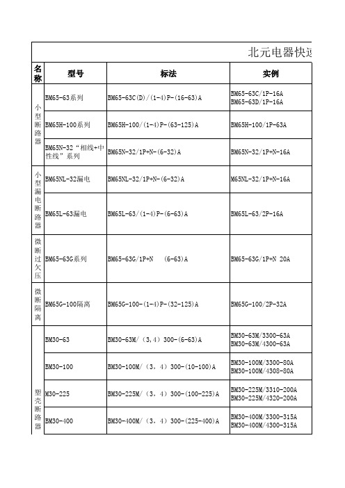
型号
标法
BM65-63系列
BM65-63C(D)/(1-4)P-(16-63)A
小
型
断 BM65H-100系列 BM65H-100/(1-4)P-(63-125)A
路
器
BM65N-32“相线+中 性线”系列
BM65N-32/1P+N-(6-32)A
北元电器快速选型表
实例
BM65-63C/1P-16A BM65-63D/1P-16A
BM30E-100/3400 -(10-100)A
BM30L-100/3400B-80A
BM30E-225/3400-(100-250)A BM30E-400/3400-(200-400)A BM30E-630/3400-(400-630)A
BM30L-225/3400B-200A BM30L-400/3400B-350A BM30L-630/3400B-500A
过载、短路、漏电 保护
用于交流50Hz线路,230V
6A、10A、16A、20A、 对建筑和类似场所
25A、32A、40A、50A、 有过载,短路,过 用于交流50Hz线路,230V
63A
欠压保护。
32A、63A、80A、100A、 隔离
用于交流50Hz或60Hz线路,400V以下
6A、10A、16A、20A、 25A、32A、40A、50A、 63A
操作和柜外操作
故障危害。
4000A、5000A、6300A
M65NL-32/1P+N-16A BM65L-63/2P-16A BM65-63G/1P+N 20A BM65G-100/2P-32A
BM30-63
BM30-63M/(3,4)300-(6-63)A
EM565161中文资料(Etron Technology)中文数据手册「EasyDatasheet - 矽搜」

5
70纳秒 70纳秒 70纳秒 55纳秒 55纳秒 55纳秒
I DDS2
25 µA 25 µA 80 µA 35 µA 35 µA 80 µA
包
G
DQ 15
NC
A12
A13
W E#
DQ 7
EM565161BJ-70 EM565161BA-70 EM565161BA-70E EM565161BJ-55 EM565161BA-55 EM565161BA-55E
L Read L H L H H L L Hale Waihona Puke rite L H X L H L L
输出禁用
UB#
L L H L L H X H X X H
DQ0~DQ7
DOUT
高阻
DQ8~DQ15
DOUT DOUT
高阻
Power
IDDO IDDO IDDO IDDO IDDO IDDO IDDO IDDO
DOUT DIN
芯片中文手册,看全文,戳
EM565161
A0
记忆 单元阵列
VDD GND
5 12 k x 1 6 A18
SENSE AMP
W E# UB#
LB# OE# CE1# CE2
初稿
2
修订版0.9
2002年1月
芯片中文手册,看全文,戳
EM565161
Mode CE1# CE2 OE# WE# LB#
80
*典型值在T测量
a
= 25°C.
电容(钽 = 25°C; F = 1兆赫)
参数 输入电容 输入/输出电容 符号
Min
Max
8 10
Unit
pF pF
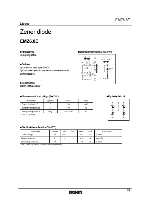
EMZ6.8E中文资料
The products listed in this document are designed to be used with ordinary electronic equipment or devices (such as audio visual equipment, office-automation equipment, communications devices, electrical appliances and electronic toys). Should you intend to use these products with equipment or devices which require an extremely high level of reliability and the malfunction of with would directly endanger human life (such as medical instruments, transportation equipment, aerospace machinery, nuclear-reactor controllers, fuel controllers and other safety devices), please be sure to consult with our sales representative in advance. About Export Control Order in Japan Products described herein are the objects of controlled goods in Annex 1 (Item 16) of Export Trade Control Order in Japan. In case of export from Japan, please confirm if it applies to "objective" criteria or an "informed" (by MITI clause) on the basis of "catch all controls for Non-Proliferation of Weapons of Mass Destruction.
NE566中文资料

April 15, 1992
399
Philips Semiconductors Linear Products
Product specification
Function generator
NE/SE566
DC ELECTRICAL CHARACTERISTICS
TA=25°C, VCC=±6V, unless otherwise specified. SYMBOL General TA VCC ICC VCO1 fMAX Maximum operating frequency Frequency drift with temperature Frequency drift with supply voltage Control terminal input impedance2 FM distortion (±10% deviation) Maximum sweep rate Sweep range Output Triangle wave output impedance voltage linearity Square wave input impedance voltage duty Cycle tR tF Rise time Fall Time 5 45 50 5.4 50 20 50 55 5 40 50 5.4 50 20 50 60 Ω VP-P % ns ns 1.9 50 2.4 0.2 1.9 50 2.4 0.5 Ω VP-P % 1 500 0.1 1 0.2 1 10:1 0.75 1 1 600 0.2 1 0.4 1 10:1 1.5 2 MHz ppm/°C %/V MΩ % MHz Operating ambient temperature range Operating supply voltage Operating supply current -55 ±6 7 125 ±12 12.5 0 ±6 7 70 ±12 12.5 °C V mA PARAMETER SE566 Min Typ Max Min NE566 Typ Max UNIT
- 1、下载文档前请自行甄别文档内容的完整性,平台不提供额外的编辑、内容补充、找答案等附加服务。
- 2、"仅部分预览"的文档,不可在线预览部分如存在完整性等问题,可反馈申请退款(可完整预览的文档不适用该条件!)。
- 3、如文档侵犯您的权益,请联系客服反馈,我们会尽快为您处理(人工客服工作时间:9:00-18:30)。
Etron Technology, Inc.No. 6, Technology Rd. V, Science-Based Industrial Park, Hsinchu, Taiwan 30077, R.O.C. 1M x 16 Pseudo SRAMPreliminary, Rev 0.2Apr. 2002Features• Organized as 1M words by 16 bits • Fast Cycle Time : 70ns • Standby Current : 100uA• Deep power-down Current : 10uA (Memory cell data invalid)• Byte data control: LB# (DQ0 - 7), UB# (DQ8 - 15) • Compatible with low power SRAM• Single Power Supply Voltage : 3.0V ±0.3V • Package Type : 48-ball FBGA, 6x8mmPin DescriptionSymbol Function A0 – A19 Address Inputs DQ0 – DQ15 Data Inputs/Outputs CE1# Chip Enable CE2Deep Power DownOE# Output Enable WE# Write Control LB# Lower Byte Control UB#Upper Byte ControlV CC Power Supply V SS GroundPin Assignment 48-Ball BGA, Top ViewOverviewThe EM566168 is a 16M-bit Pseudo SRAM organized as 1M words by 16 bits. It is designed with advanced CMOS technology specified RAM featuring low power static RAM compatible function and pin configuration. This device operates from a single power supply. Advanced circuit technology provides both high speed and low power. It is automatically placed in low-power mode when CS1# or both UB# and LB# are asserted high or CS2 is asserted low. There are three control inputs. CS1# and CS2 are used to select the device, and output enable (OE#) provides fast memory access. Data byte control pins (LB#,UB#) provide lower and upper byte access. This device is well suited to various microprocessor system applications where high speed, low power and battery backup are required. And, with a guaranteed wide operating range, the EM566168 can be used in environments exhibiting extreme temperature conditions.Pin LocationSymbol Location Symbol Location Symbol Location Symbol Location Symbol Location Symbol Location A0 A3 A8 H2 A16 E4 DQ3 D5 DQ11 D2 WE# G5 A1 A4 A9 H3 A17 D3 DQ4 E5 DQ12 E2 LB# A1 A2 A5 A10 H4 A18 H1 DQ5 F5 DQ13 F2 UB# B2 A3 B3 A11 H5 A19 G2 DQ6 F6 DQ14 F1 VCC D6 A4 B4 A12 G3 NC H6 DQ7 G6 DQ15 G1 VCC E1 A5 C3 A13 G4 DQ0 B6 DQ8 B1 CE1# B5 GND D1 A6 C4 A14 F3 DQ1 C5 DQ9 C1 CE2 A6 GND E6 A7 D4 A15 F4 DQ2 C6 DQ10 C2 OE# A2 NC E3654321LB# OE# DQ8 UB# A0 A1 A3 A4 A2 CE2CE1# DQ0DQ9 DQ10 VSS DQ11 A5 A6 A17 A7 DQ1 DQ2DQ3 VCCVCC DQ12 DQ14 DQ13 NC A16 A14 A15 DQ4 VSSDQ5 DQ6DQ15A19A18A8A12A13A9A10WE#DQ7A11NCGHFEDCBABlock DiagramAddress BufferRow Address DecoderMemory Cell Array1M x 16Input Data ControlSense AMP Column DecoderStandby/Deep Power Down Mode ControlRefresh ControlRefresh CounterOutput Data ControlAddress BufferControl LogicVCC VSSA0 – A19DQ0 – DQ7 DQ8 – DQ15 CS1# CS2 LB# OE# WE# UB#Operating ModeCS1# CS2 OE# WE# LB# UB# DQ0~DQ7 DQ8~DQ15 Mode PowerH H X X X X High-Z High-Z Deselect StandbyPowerDown X L X X X X High-Z High-Z Deselect DeepL H X X H H High-Z High-Z Deselect StandbyDisabled Active L H H H L X High-Z High-Z OutputDisabled Active L H H H X L High-Z High-Z OutputByteRead Active L H L H L H D-out High-Z LowerByteRead Active L H L H H L High-Z D-out UpperRead Active L H L H L L D-out D-out WordWrite Active L H X L L H D-in High-Z LowerByteWrite ActiveByteL H X L H L High-Z D-in UpperWrite Active L H X L L L D-in D-in WordNote: X=don’t care. H=logic high. L=logic low.Absolute Maximum Ratings1)Supply voltage, V CC-0.2 to +3.6VInput voltages, V IN-0.2 to VCC + 0.3VInput and output voltages, V IN, V OUT-2.0 to +3.6V*mAOutput short circuit current I SH 100Operating temperature, T A-25 to +85°CStorage temperature, T STRG-65 to +125°CSoldering Temperature (10s), T SOLDER240°CWPower dissipation, P D 1Note: Absolute maximum DC requirements contains stress ratings only. Functional operation at the absolute maximum limits is not implied or guaranteed. Extended exposure to maximum ratings may affect device reliability.Recommended DC Operating ConditionsUnitMax.Typ.Symbol Parameter Min.V CC Power Supply Voltage 2.7 3.0 3.3 VV SS Ground 0 −0 V V IH Input High Voltage 2.2 −V CC+0.21) V V IL Input Low Voltage -0.22)−+0.6 V Notes:1. Overshoot: VCC +2.0V in case of pulse width ≤ 20ns2. Undershoot: -2.0V in case of pulse width ≤ 20ns3. Overshoot and undershoot are sampled, not 100% tested.DC CharacteristicsSymbol Parameter TestConditionsMin.Max.UnitI LI Input Leakage Current V IN = V SS to V DD-1 1 µAI LO Output Leakage Current V IO = V SS to V DDCE1# = V IH, CE2 = V IL orOE# = V IH or WE# = V IL-1 1 µAI CC1Operating Current @ MinCycle TimeCycle time = Min., 100% dutyI IO = 0mA, CE1# = V IL,CE2 = V IH, V IN = V IH or V IL−25 mAI CC2Operating Current @ MaxCycle Time (1µs)Cycle time = 1µs, 100% dutyI IO = 0mA, CE1# ≤ 0.2V,CE2 ≥ V DD-0.2V, V IN ≤ 0.2Vor V IN ≥ V DD-0.2V− 3 mAI SB1Standby Current (CMOS) CE1# = V DD – 0.2V andCE2 = V DD – 0.2V,Other inputs = V SS ~ V CC−100 µAI SBD Deep Power Down CE2≤ 0.2V, Other inputs =V SS ~ V CC10 µAV OL Output Low Voltage I OL = 2.1mA −0.4 V V OH Output High Voltage I OH = -1.0mA 2.4 −VCapacitance (Ta = 25°C; f = 1 MHz)Parameter SymbolMinTypMaxUnitTestConditionsInput capacitance C IN−−8 pF V IN = GNDOutput capacitance C OUT−−10 pF V OUT = GNDNotes: These parameters are sampled and not 100% tested.AC Characteristics and Operating Conditions (Ta = -25°C to 85°C, V CC = 2.7V to 3.3V)-85 -70Unit Symbol ParameterMin Max Min MaxRead Cyclet RC Read cycle time 85 −70 −ns t AA Address access time −85 −70 ns t CO1Chip Enable (CE1#) Access Time −85 −70 ns t CO2Chip Enable (CE2) Access Time −85 −70 ns t OE Output enable access time −40 −35 ns t BA Data Byte Control Access Time −85 −70 ns t LZ Chip Enable Low to Output in Low-Z 10 −10 −ns t OLZ Output enable Low to Output in Low-Z 5 − 5 −ns t BLZ Data Byte Control Low to Output in Low-Z 10 −10 −ns t HZ Chip Enable High to Output in High-Z −35 −25 ns t OHZ Output Enable High to Output in High-Z −35 −25 ns t BHZ Data Byte Control High to Output in High-Z −35 −25 ns t OH Output Data Hold Time 10 −10 −nsWrite Cyclet WC Write Cycle Time 85 −70 −ns t WP Write Pulse Width 60 −50 −ns t AW Address Valid to End of Write 70 −60 −ns t CW Chip Enable to End of Write 70 −60 −ns t BW Data Byte Control to End of Write 70 −60 −ns t AS Address Setup Ttime 0 −0 −ns t WR Write Recovery Time 0 −0 −ns t WHZ WE# Low to Output in High-Z −30 −20 ns t OW WE# High to Output in Low-Z 5 − 5 −ns t DW Data to Write Overlap 30 −30 −ns t DH Data Hold Time 0 −0 −ns AC Test Condition• Output load : 50pF + one TTL gate• Input pulse level : 0.4V, 2.4• Timing measurements : 0.5 x V CC• tR, tF : 5nsAC Test LoadsNote:1. Including scope and jig capacitanceState DiagramStandby Mode CharacteristicsPower Mode Memory Cell DataStandby Current (µA)Wait Time (µs)Standby Valid 1000 Deep Power DownInvalid10200C L 1= 50 pFV L = 1.5 VR L = 50 ΩZ 0 = 50 ΩD OUT CE1# =VIH orVIL, CE2=VIH CE2=VIL CE1# = VIH or VIL,CE2=VIHCE2=VIL CE2=VIH, CE1# =VIHor UB#, LB# =VIH CE1# =VIL, CE2=VIH, UB# & LB# or/and LB# = VIL Power on Initial State (Wait 200µs) Active Deep Power Down ModeStandbyMode Power Up Sequence Deep Power Down Exit SequenceTiming DiagramsRead Cycle 1 – Addressed Controlled1)Read Cycle 2 – CS1# Controlled2)Notes:1. CE1# = OE# = V IL , CE2 = WE# = V IH , UB# or/and LB# = V IL2. CE2 = WE# = V IHtRCAddressData OuttOHtOHPrevious Data ValidData ValidtAAtRCAddresstOHData OuttAA tCOtLZCE1#UB#, LB#tBAtBLZtOEtOLZOE#High-ZHigh-ZData ValidtHZtBHZtOHZWrite Cycle 1 – WE# Controlled 1) 2)Write Cycle 2 – CS1# Controlled 1) 2)tWCAddresstWRData IntAWtCWCE1#UB#, LB#tBWtASWE#High-ZHigh-ZData ValidtDHData UndefinedData OuttWPtDW tOWtWCAddresstWRData In tAWtCWCE1#UB#, LB#tBWtASWE#Data ValidtDHData OuttWPtDWHigh-ZtWHZWrite Cycle 3 – UB#, LB# Controlled 1) 2)Notes:1. CE2 = V IH2. CE2 = WE# = V IHtWCAddresstWRData In tAWtCWCE1#UB#, LB#tBWtASWE#Data ValidtDHData OuttWPtDWHigh-ZDeep Power Down ModePower Up 1Power Up 2 (No Dummy Cycle)Normal Operation 1µs==Normal OperationSuspend200µsWake UpRead Operation Twice or Stay High during 300µsDeep Power Down ModeCE2ModeCE1#=200µs=200µs=300µsRead Operation TiwceV CCCE2CE1#V CCCE2CE1#Avoid TimingEtron Pseudo SRAM has a timing which is not supported at read operation. If your system has multipleinvalid address signal shorter than tRC during over 15µs at read operation shown as in Abnormal Timing, it requires a normal read timing at leat during 15 µs shown as in Avoidable timing 1 or toggle CE1# to high ( tRC) one time at least shown as in Avoidable Timing 2.Abnormal TimingAvoidable Timing 1Avoidable Timing 2CE1#WE#Address 15µs< tRCCE1#WE#Address 15µstRCCE1#WE#Address15µs< tRCtRCPackage Diagrams 48-Ball BGA Units in mm654321123456TO P V IE WP IN 1 C O R N E RB O TTO M V IE W0.30 0.05(48X)0.15SS C CA BPIN 1 C O RN ER0.753.75- B -- A -- C -S E ATIN G P L AN E0.12M AX50.150.0756.0 ² 0.18.0 ² 0.11.20 M A X0.52 ² 0.020.32 ² 0.040.23 ² 0.03。