AN2659(V1)STM8S如何用定制的编程器进行IAP
AN2659 STM8 in_application programming (IAP) using a customized user_bootloaderV4.1
November 2012Doc ID 14153 Rev 41/25AN2659Application noteSTM8 in-application programming (IAP)using a customized user-bootloaderIntroductionThis application note is intended for STM8 firmware and system designers who need to implement an in-application programming (IAP) feature in the product they are developing with the STM8 microcontroller.The STM8 is an 8-bit microcontroller family with a Flash memory for storing the user program code or firmware. IAP makes it possible to update the firmware ‘in situ’, after the microcontroller has been embedded in the final product. The advantage is that the microcontroller board can stay inside its product enclosure. No mechanical intervention is needed to make the update.IAP is extremely useful for distributing new firmware versions. It makes it easy to add new product features and correct problems throughout the product life cycle.The user-bootloader firmware source code provided with this application note shows an example of how to implement IAP for the STM8 microcontroller. Use this code as a reference when integrating IAP in your STM8 application. It includes the following features:●Bootloader activated by external pin (jumper on PCB)●Flash block programing by executable RAM code management ●Read while write (RWW) feature ●High level C-language usage ●Reduced size of the code (optimized code) ●Support for multiple communication interfaces (SPI, I 2C, and UART)●UART code compatible with ST Flash loader demonstrator software Table 1.Applicable productsProduct family Part numbersMicrocontrollers –STM8S003xx, STM8S005xx, STM8S007C8–STM8S103xx, STM8S903xx, STM8S105xx, STM8S207xx, STM8S208xx,–STM8AF6x26/4x/66/68, STM8AF5xxx, STM8AF6x69/7x/8x/9x/Ax–STM8L05xxx–STM8L101xx–STM8L151C2/K2/G2/F2 and STM8L151C3/K3/G3/F3–STM8L151x4, STM8L151x6, STM8L152x4, STM8L152x6–STM8L151x8, STM8L152x8, STM8L151R6, STM8L152R6, STM8L162R8,STM8L162M8–STM8AL313x, STM8AL314x, STM8AL316x, STM8AL3L4x, STM8AL3L6x–STM8TL5xxx Contents AN2659Contents1Operation theory . . . . . . . . . . . . . . . . . . . . . . . . . . . . . . . . . . . . . . . . . . . . 52STM8 devices with built-in ROM-bootloader . . . . . . . . . . . . . . . . . . . . . 62.1Implementation details . . . . . . . . . . . . . . . . . . . . . . . . . . . . . . . . . . . . . . . . 62.2Adapting IAP master side to ROM-bootloader protocol . . . . . . . . . . . . . . . 73User-bootloader for STM8 devices . . . . . . . . . . . . . . . . . . . . . . . . . . . . . 83.1User-bootloader firmware example description . . . . . . . . . . . . . . . . . . . . . 93.2Configuring the user-bootloader firmware example . . . . . . . . . . . . . . . . . 124Memory management for IAP . . . . . . . . . . . . . . . . . . . . . . . . . . . . . . . . . 134.1Memory protection . . . . . . . . . . . . . . . . . . . . . . . . . . . . . . . . . . . . . . . . . . 134.1.1Flash memory protection . . . . . . . . . . . . . . . . . . . . . . . . . . . . . . . . . . . . 134.1.2User boot code protection (UBC) . . . . . . . . . . . . . . . . . . . . . . . . . . . . . . 134.1.3Vector table redirection . . . . . . . . . . . . . . . . . . . . . . . . . . . . . . . . . . . . . 144.2Block versus word programming . . . . . . . . . . . . . . . . . . . . . . . . . . . . . . . 154.3RAM versus Flash programming code location . . . . . . . . . . . . . . . . . . . . 154.3.1Programming the data EEPROM area . . . . . . . . . . . . . . . . . . . . . . . . . . 154.4Library support for Flash programming . . . . . . . . . . . . . . . . . . . . . . . . . . 164.4.1Flash programming function list . . . . . . . . . . . . . . . . . . . . . . . . . . . . . . . 165Configuring the Cosmic compiler for RAM code execution . . . . . . . . 185.1Creating a segment in the STVD project . . . . . . . . . . . . . . . . . . . . . . . . . 185.2Creating a memory segment in the Cosmic linker file . . . . . . . . . . . . . . . 195.3Finishing and checking the configuration . . . . . . . . . . . . . . . . . . . . . . . . . 20 6Setting up your application firmware for user-bootloader use . . . . . . 227Conclusion . . . . . . . . . . . . . . . . . . . . . . . . . . . . . . . . . . . . . . . . . . . . . . . . 237.1Features in the final user-bootloader application . . . . . . . . . . . . . . . . . . . 23 8Revision history . . . . . . . . . . . . . . . . . . . . . . . . . . . . . . . . . . . . . . . . . . . 242/25Doc ID 14153 Rev 4AN2659List of tables List of tablesTable 1.Applicable products . . . . . . . . . . . . . . . . . . . . . . . . . . . . . . . . . . . . . . . . . . . . . . . . . . . . . . . 1 Table 2.Document revision history . . . . . . . . . . . . . . . . . . . . . . . . . . . . . . . . . . . . . . . . . . . . . . . . . 24Doc ID 14153 Rev 43/25List of figures AN2659 List of figuresFigure 1.Typical bootloader application . . . . . . . . . . . . . . . . . . . . . . . . . . . . . . . . . . . . . . . . . . . . . . . 5 Figure 2.Example of STM8S208xx bootloader. . . . . . . . . . . . . . . . . . . . . . . . . . . . . . . . . . . . . . . . . . 6 Figure 3.Example of user-bootloader implementation in the Flash memory. . . . . . . . . . . . . . . . . . . . 8 Figure 4.Example of the user-bootloader package provided . . . . . . . . . . . . . . . . . . . . . . . . . . . . . . . 9 Figure 5.Bootloader flowchart. . . . . . . . . . . . . . . . . . . . . . . . . . . . . . . . . . . . . . . . . . . . . . . . . . . . . . 11 Figure er boot code area and user application area . . . . . . . . . . . . . . . . . . . . . . . . . . . . . . . . . 14 Figure 7.Define linker memory section in STVD. . . . . . . . . . . . . . . . . . . . . . . . . . . . . . . . . . . . . . . . 19 Figure 8.Setting the project start and vector table addresses in STVD . . . . . . . . . . . . . . . . . . . . . . 22 4/25Doc ID 14153 Rev 4AN2659Operation theory Doc ID 14153 Rev 45/251 Operation theoryIn practice, IAP requires a bootloader implemented in the STM8 firmware that cancommunicate with an external master (such as a PC) via a suitable communicationinterface. The new code can be downloaded into the microcontroller through this interface.The microcontroller then programs this code into its Flash memory.IAP can also be used to update the content of the internal data EEPROM memory, and theinternal RAM memory.This operation is useful when a microcontroller is already soldered in its final application andneeds a firmware update.Figure 1 shows a typical bootloader application.Figure 1.Typical bootloader applicationThe bootloader is that part of the code which runs immediately after a microcontroller resetand which waits for an activation signal (for example, from grounding a specific pin orreceiving a token from a communication interface). If activation is successful the code entersbootloader mode. If activation fails (for example due to a timeout or the jumper on the pin notbeing present) the bootloader jumps directly to the user application code.In bootloader mode, the microcontroller communicates with the external master devicethrough one of the serial communication interfaces available in it (UART, SPI, I 2C, CAN)using a set of commands. These commands are usually:●Write to Flash ●Erase Flash ●Verify Flash ●Additional operations such as read memory and execute code from a given address (jump to given address).The ST proprietary bootloader can be used. It is embedded in the ROM memory of STM8devices with a program memory greater than 8 Kbytes. In this case, no code development isneeded. To use the proprietary bootloader, enable it via the option bytes.Alternatively, develop a customized bootloader using, for example, a serial communicationinterface that is not supported in ST versions or in devices where the ST bootloader is notpresent. Such a bootloader should be stored in the user boot code area (UBC) in themicrocontroller. This guarantees protection against unintentional write operations.RS232RS232/TTLconverterSTM8 boardSTM8Bootloader enable PC jumper2 STM8 devices with built-in ROM-bootloaderMost STM8 devices have an internal bootROM memory which contains an ST proprietarybootloader. Consequently, they already have a built in IAP implementation (see UM0560:STM8 bootloader).details2.1 ImplementationThe built-in ROM-bootloader is located in a dedicated part of the memory called theBootROM. The ROM-bootloader code is fixed (not rewritable) and is specific for eachdevice. The communication interface supported depends on the peripherals present in thegiven STM8 device and whether they are implemented in the ROM-bootloader. For example,some devices support firmware download through UART/LIN and CAN, some devicessupport only UART, and others only SPI. Information concerning the supported interfacescan be found in the relevant device datasheet.Activation of the built-in ROM-bootloader is made by programming the BL[7:0] option bytedescribed in the option byte section of the device datasheet. The bootROM bootloaderchecks this option byte and if it is enabled, it runs its own code (it waits for the host to sendcommands/data). If the BL[7:0] option byte is inactive, the bootrom bootloader jumps to theuser reset address (0x8000).6/25Doc ID 14153 Rev 42.2 Adapting IAP master side to ROM-bootloader protocolTo be able to download firmware into the device, the host and bootloader must communicatethrough the same protocol. This bootloader protocol for STM8 devices is specified in theSTM8 bootloader (UM0560) user manuals available from . The sameprotocol is used in the firmware example provided with this application note. The UM0560user manual describes all bootloader protocol properties including used interfaces,timeouts, command formats, packet formats, and error management.Doc ID 14153 Rev 47/253 User-bootloader for STM8 devicesFor STM8 microcontrollers which do not include a built-in bootloader or which use acommunication protocol (I2C) not yet supported in the built-in bootloader, user-bootloaderfirmware can be added and customized at the beginning of the Flash memory.For this purpose, an example of a user-bootloader firmware is provided with this applicationnote. This package is divided into three main subdirectories, each one dedicated to oneSTM8 family member: STM8AF, STM8L and STM8S. For the STM8AL family, please usethe STM8L directory. Each directory is composed of the following components:●Sources: containing the firmware source code●Includes: containing the firmware header file (main.h). This file can be edited toconfigure your user-bootloader (see Section 3.2: Configuring the user-bootloaderfirmware example).●Flash_loader_demonstrator_files: contain all map files to add in the Flashloaderdemonstrator install directory to be compatible with the user-bootloader.●STVD: containing a prebuilt project for STVD using a Cosmic or raisonance compilerFigure 4 shows an example of the user-bootloader firmware.8/25Doc ID 14153 Rev 4Figure 4.Example of the user-bootloader package providedfirmware example description3.1 User-bootloaderThe basic program flow of a user bootloader application is described in Figure 5: Bootloaderflowchart.After a device reset, a selected GPIO can be used as a bootloader activation signal.Depending on its logical state (0 V or 5 V), the bootloader can be activated or not.The bootloader configures this GPIO as input mode with pull-up in order to detect anyvoltage variation. If the pin voltage level is zero (jumper present), the bootloader is activated.Otherwise, the bootloader jumps to the reset address of the user application (if this addressis valid).In the case of bootloader activation, the chosen communication interface is initialized. Atimeout count is then activated (i.e. 1 second). If, during this timeout, nothing is receivedfrom the given communication interface (UART, SPI, I2C) the bootloader jumps to the userapplication reset address.If the user-bootloader receive a valid activating token byte from the communication interfacebefore the timeout elapses, it then enters memory management mode to perform thefollowing operations:1.Initialize the Flash programming routines by copying the programming functions toRAM.2. Wait in a loop for a valid command to be received from the master3. Compute the received command (read, write, erase, version)4. If a Go command is received, the user-bootloader jumps to the address given in thecommand.All commands have a specified format and must be followed by both the user-bootloaderand the master. The command specification handles all possibilities and covers errormanagement.Doc ID 14153 Rev 49/25Several specific processing methods must be taken into account to achieve the appropriateaction in the memory using the bootloader. These methods are explained in Section 4:Memory management for IAP. They include:●Protection management●Code execution from RAM depending on memory write method (byte, word, or blockprogramming).10/25Doc ID 14153 Rev 4Doc ID 14153 Rev 411/25Figure 5.Bootloader flowchartReset IO pin groundedInit I/O pin (pull-up)Y es User application start Valid user reset vector?Received tokenin timeout interval?Perform commandWait for command from MasterGO command?(to run user code)Jump to GO address Parse commands- WRITE- ERASE- READ- VERSIONCopy write block routine into RAMCommunicationinterface init protocol No No NoNoY es Y esY es3.2 Configuring the user-bootloader firmware exampleThe provided package is configured for STM8S105xx devices with I2C protocol. Thepackage can be reconfigured easily, without any source code modification, by modifyinginformation in the main.h files (see package description).The configuration file is divided into three sections (see below). Each section can bemodified depending on requirements./* USER BOOTLOADER PROTOCOL PARAMETERS */This section is used to select a protocol. The user-bootloader firmware example supportsthree protocols: UART, I2C, and SPI. Only one protocol can be selected./* USER USER BOOT CODE Customisation */This section is used for defining byte values (acknowledge, non-acknowledge, andidentification), command numbers, and received data buffer structure./* USER BOOT CODE MEMORY PARAMETERS */This section is used to describe the memory configuration of the STM8 microcontroller. It ismandatory to set up some memory variables corresponding to the memory configuration ofthe microcontroller, for example, memory size, block size, EEPROM size, and addressrange. For more informations on these variables please refer to the appropriate devicedatasheet).12/25Doc ID 14153 Rev 44 Memory management for IAPprotection4.1 Memoryprotection4.1.1 FlashmemoryTo avoid accidental overwriting of the Flash code memory (for example in the case of afirmware crash) several levels of write protection are implemented in the STM8microcontroller family.After an STM8 reset, write access to the Flash memory is disabled. To enable it, firmwaremust write two unlock keys in a dedicated register. If the unlock keys are correct (0x56,0xAE), write access to the Flash memory is enabled and it is possible to program the Flashmemory using either byte/word or block programming mode. If the unlock keys are incorrect,write access to the Flash memory is disabled until the next device reset. After writing to theFlash memory, it is recommended to enable write protection again by clearing a specific bitin the Flash control register (to avoid accidental write). A similar protection mechanismexists for the Data EEPROM memory, with a specific unlock register and unlock keys (0xAE,0x56).code protection (UBC)boot4.1.2 UserAdditional write protection exists for the programming code itself, to protect the user-bootloader code from being overwritten during IAP. The STM8 family has a user boot code(UBC) area which is permanently write protected. This UBC area starts from the Flashmemory start address (0x8000) and its size can be changed by the UBC option byte (seedevice reference manuals and product datasheets). The boot code area also includes aninterrupt vector table (0x8000 to 0x8080). An important point to highlight in order to modifythe vector table via IAP, is that the main vector table should be redirected to another vectortable located in the rewritable application code area (see Figure 6). The only drawback ofsuch redirection, is the increase of the interrupt latency because of the execution of a doublejump.Doc ID 14153 Rev 413/25More detailed information about memory map of specific STM8 device type can be found inthe STM8 reference manuals and datasheets.redirectiontable4.1.3 VectorAs the initial interrupt vector table (address 0x8000 to 0x8080) is write protected by the UBCoption, it is mandatory to create another interrupt vector table to be able to modify it by IAP.Vector table redirection is performed in the following way:●The start of the user application area contains its own interrupt table with the sameformat as the primary interrupt table.●The primary interrupt table contains a set of jumps to the user interrupt table. If aninterrupt occurs, the user application is automatically redirected from the primaryinterrupt table to the user interrupt table by one jump.●The only requirement for the user application is that the user interrupt table must belocated at a fixed address. This is because the primary interrupt table is not rewritableand jumps to the user interrupt table at a fixed address value (see Section 6: Setting upyour application firmware for user-bootloader use).14/25Doc ID 14153 Rev 44.2 Block versus word programmingSTM8 microcontrollers contain a Flash type program memory where firmware can bewritten. There are two methods for writing (or erasing) Flash program memory:●Byte/word programming (1 or 4 bytes)–Advantages: offers small area programming, code can be executed directly on the Flash program.–Disadvantages: program stops during programming, programming speed is slow●Block programming (128 bytes or 1 Flash block for a given STM8 device)–Advantages: offers large area programming with high speed (large blocks)–Disadvantages: programming routine must run from the RAM (need to copyprogramming routine into the RAM).4.3 RAM versus Flash programming code locationDepending on the selected programming method (see Section 4.2: Block versus wordprogramming), the programming code must run from the RAM or from the Flash memory.If the programming code runs from the Flash memory, use only byte/word programming toprogram the Flash memory. During Flash memory programming, the code cannot accessthe Flash memory (the Flash is in programming mode). Therefore, program execution fromthe Flash is stopped during programming (for several milliseconds) and then continues. Thismode is useful in situations where only a small part (a few bytes) of the Flash memoryneeds to be updated or when it does not matter that programming is (very) slow.To program a large Flash memory area with optimum speed, block programming mode hasto be used. Block programming mode can be performed only by a code located in the RAM.First, copy the programming code into the RAM and then run (jump to) this code. The RAMcode can then use block mode to program the Flash. In this mode, programming one blocktakes the same time as programming one byte/word in byte/word mode. Consequently,programming speed is faster and code execution is not stopped (because it is running fromRAM). The only disadvantage of this method is the RAM code management:–Copying the executable code to the RAM–Storing the RAM code–Allocating RAM space for the code–Compiling the code to be able to run from the RAMdata EEPROM areathe4.3.1 ProgrammingFor data EEPROM programming, the programming code does not have to be executed fromthe RAM. It can be located in the Flash program memory, even if block programming isused. This read-while-write (RWW) feature speeds up microcontroller performance duringIAP. Only the data loading phase, the part of code which loads data into the EEPROM buffer,must execute from the RAM. However, during the physical programming phase, which takesmore time (several milliseconds), the code runs from the Flash while the data EEPROMmemory is programmed in the background. Completion of data EEPROM programming isindicated by a flag. An interrupt can be generated when the flag is set.Doc ID 14153 Rev 415/254.4 Library support for Flash programmingThe STM8 firmware libraries, available from , provide developed and verifiedfunctions for programming the Flash memory of every STM8 microcontroller family. Thefunctions support byte/word and block programming and make it easier for developers towrite their own programming code. The library also includes functions for managing theprogramming code execution from RAM. These functions are: copy to RAM, execution fromRAM, and storing functions in the Flash memory. They are contained in the following files:●\library\scr\stm8x_flash.c●\library\inc\stm8x_flash.hThese files contain the complete source code for Flash programming. Refer to the libraryuser manual “\FWLib\stm8s_fwlib_um.chm” for help using the STM8 library.4.4.1 Flash programming function listThis list gives a short description of the STM8S Flash programming functions (which are thesame for STM8AF, STM8AL, and STM8L devices):void FLASH_DeInit ( void)Deinitializes the FLASH peripheral registers to their default reset values.void FLASH_EraseBlock ( u16 BlockNum, FLASH_MemType_TypeDef MemType ) Erases a block in the program or data EEPROM memory.void FLASH_EraseByte ( u32 Address )Erases one byte in the program or data EEPROM memory.void FLASH_EraseOptionByte ( u32 Address )Erases an option byte.u32 FLASH_GetBootSize ( void )Returns the boot memory size in bytes.FlagStatus FLASH_GetFlagStatus ( FLASH_Flag_TypeDef FLASH_FLAG )Checks whether the specified Flash flag is set or not.FLASH_LPMode_TypeDef FLASH_GetLowPowerMode ( void )Returns the Flash behavior type in low power mode.FLASH_ProgramTime_TypeDef FLASH_GetProgrammingTime ( void )Returns the fixed programming time.void FLASH_ITConfig ( FunctionalState NewState )Enables or disables the Flash interrupt mode.void FLASH_Lock ( FLASH_MemType_TypeDef MemType )Locks the program or data EEPROM memory.void FLASH_ProgramBlock ( u16 BlockNum, FLASH_MemType_TypeDef MemType, FLASH_ProgramMode_T ypeDef ProgMode, u8 * Buffer )Programs a memory block.void FLASH_ProgramByte ( u32 Address, u8 Data )Programs one byte in the program or data EEPROM memory.void FLASH_ProgramOptionByte ( u32 Address, u8 Data )Programs an option byte.16/25Doc ID 14153 Rev 4void FLASH_ProgramWord ( u32 Address, u32 Data )Programs one word (4 bytes) in the program or data EEPROM memory.u8 FLASH_ReadByte ( u32 Address )Reads any byte from the Flash memory.u16 FLASH_ReadOptionByte ( u32 Address )Reads one option byte.void FLASH_SetLowPowerMode ( FLASH_LPMode_TypeDef LPMode )Select the Flash behavior in low power mode.void FLASH_SetProgrammingTime ( FLASH_ProgramTime_TypeDef ProgTime )Sets the fixed programming time.void FLASH_Unlock ( FLASH_MemType_T ypeDef MemType )Unlocks the program or data EEPROM memory.FLASH_Status_TypeDef FLASH_WaitForLastOperation ( FLASH_MemT ype_T ypeDef MemT ype )Waits for a Flash operation to complete.Note:The STM8 library package also contains examples that show how to use these functions in the final source code. Write your own code based on these examples.Doc ID 14153 Rev 417/255 Configuring the Cosmic compiler for RAM codeexecutionBlock programming must be executed from the RAM memory. Therefore, the code to becopied into the RAM must be compiled and linked to be run in the RAM address space but itis stored in the Flash memory.It is possible to write a simple programming code assembly, taking care with the RAMaddressing and then storing this code in the Flash (example, the code uses only relativeaddressing or RAM addresses). However, it is more efficient to use compiler support for thispurpose. Cosmic compiler support (described below) has these features built-in. Twoprocessing methods can be used:●Creating a segment in the STVD project●Creating a memory segment in the Cosmic linker file5.1 Creating a segment in the STVD projectThe first step to create a segment in the STVD project is to define one section in your code,example “FLASH_CODE”, and put your Block programming function inside. This is doneusing the following code:...//set code section to FLASH_CODE placement#pragma section (FLASH_CODE)void FlashWrite(void){...}void FlashErase(void){...}//set back code section to default placement#pragma section ()...The second step is to set the linker in your project settings window by clicking onProject>Settings, then clicking on access to Linker tab, and then selecting “input”category. In this way you can dedicate a memory area to your defined section,“.FLASH_CODE”, in the RAM . Option “-ic” must also be associated with this section (seeFigure 7: Define linker memory section in STVD).18/25Doc ID 14153 Rev 4Figure 7.Define linker memory section in STVD5.2 Creating a memory segment in the Cosmic linker fileThe second way to configure the Cosmic compiler for RAM code execution is to create aspecial memory segment which is defined in the linker file (*.lkf) and marked by the flag “-ic”.An example of a RAM space segments definition in the linker file is as follows:# Segment Ram:+seg .data -b 0x100 -m 0x500 -n .data+seg .bss -a .data -n .bss+seg .FLASH_CODE -a .bss -n FLASH_CODE -icThis example defines a RAM space from address 0x100. Firstly, the .data and .bss sectionsare defined. Then, the code defines a moveable .FLASH_CODE section where the routinesfor Flash memory erase and write operations are located. This section must be marked byoption “-ic” (moveable code).Into the marked “-ic” section, put functions which should be compiled/linked for RAMexecution but which are stored in the Flash memory. This is done in the source code bydefining a section as shown below:Doc ID 14153 Rev 419/25...//set code section to FLASH_CODE placement#pragma section (FLASH_CODE)void FlashWrite(void){...}void FlashErase(void){...}//set back code section to default placement#pragma section ()...5.3 Finishing and checking the configurationBy using either one of the above processes (Creating a segment in the STVD project orCreating a memory segment in the Cosmic linker file), the “FlashWrite()” and “FlashErase()”functions are compiled and linked for RAM execution (in the section “FLASH_CODE”) buttheir code is placed in the Flash memory (after the“.text” and “.init” sections). This can beseen in the generated map file:Example of final map file:--------Segments--------start 00008080 end 00008500 length 1152 segment .textstart 00000000 end 00000000 length 0 segment .bsctstart 00000000 end 00000003 length 3 segment .ubsctstart 00000003 end 00000098 length 149 segment .RAMstart 00000098 end 00000098 length 0 segment .sharestart 00000100 end 00000100 length 0 segment .datastart 00000100 end 00000100 length 0 segment .bssstart 00000100 end 000001F0 length 240 segment .FLASH_CODE, initializedstart 00008510 end 00008600 length 240 segment .FLASH_CODE, fromstart 00008000 end 00008080 length 128 segment .conststart 00008500 end 00008510 length 16 segment .initThe map file shows the location of the “FLASH_CODE” sections. One section is for storagein the Flash (it is stored in the map file marked “from”). The other section is for execution (itis stored in the map file marked “initialized”).Finally, the microcontroller firmware must copy these sections from the Flash to the RAMbefore calling the RAM functions. The Cosmic compiler supports this copying by a built-infunction “int _fctcpy(char name)” which copies a whole section from a source location in theFlash to a destination location in the RAM using the following code:20/25Doc ID 14153 Rev 4。
STM8S固件库使用手册al

STM8S固件库使用手册alSTM8S固件库用户手册STM8S系列8位微控制器固件函数库version 1.1.0北京微芯力科 & 沈阳微扬电机整理INDEXSTM8S_FWLIB version V1.1.0stm8s_Adc1 __________ 1 stm8s_Beep __________ 7 stm8s_Clk __________ 8 stm8s_exti __________ 14 stm8s_flash __________ 16 stm8s_gpio __________ 20 stm8s_iwdg __________ 23 stm8s_tim1 __________ 24 stm8s_tim2 __________ 40 stm8s_tim4 __________ 50 stm8s_can __________*************************************************************** ************************** file stm8s_adc1. version V1.1.0 *************************************************************** ************************** ***************************** STM8S FWLIB *************************************** ADC1_DeInit(void);ADC1_Init( ADC1_ConvMode_TypeDef ADC1_ConversionMode,ADC1_Channel_TypeDef ADC1_Channel,ADC1_PresSel_TypeDef ADC1_PrescalerSelection,ADC1_ExtTrig_TypeDef ADC1_ExtTrigger,FunctionalState ADC1_ExtTriggerState,ADC1_Align_TypeDef ADC1_Align,ADC1_SchmittTrigg_TypeDef ADC1_SchmittTriggerChannel, FunctionalState ADC1_SchmittTriggerState);ADC1_Cmd(FunctionalState NewState);ADC1_ScanModeCmd(FunctionalState NewState);ADC1_DataBufferCmd(FunctionalState NewState);ADC1_ITConfig(ADC1_IT_TypeDef ADC1_IT, FunctionalState NewState);ADC1_PrescalerConfig(ADC1_PresSel_TypeDefADC1_Prescaler);ADC1_SchmittTriggerChannel,ADC1_SchmittTriggerConfig( ADC1_SchmittTrigg_TypeDefFunctionalState NewState);ADC1_ConversionConfig( ADC1_ConvMode_TypeDef ADC1_ConversionMode,ADC1_Channel_TypeDef ADC1_Channel,ADC1_Align_TypeDef ADC1_Align);ADC1_ExternalTriggerConfig(ADC1_ExtTrig_TypeDefADC1_ExtTrigger, FunctionalState NewState); ADC1_AWDChannelConfig(ADC1_Channel_TypeDef Channel, FunctionalState NewState);ADC1_StartConversion(void);ADC1_GetConversionValue(void);ADC1_SetHighThreshold(u16 Threshold);ADC1_SetLowThreshold(u16 Threshold);ADC1_GetBufferValue(u8 Buffer);ADC1_GetAWDChannelStatus(ADC1_Channel_TypeDef Channel);ADC1_ClearFlag(ADC1_Flag_TypeDef Flag);ADC1_GetITStatus(ADC1_IT_TypeDef ITPendingBit);ADC1_ClearITPendingBit(ADC1_IT_TypeDef ITPendingBit);*************************************************************** ***************************************************************************************** ************************** ADC1_DeInit(void);*************************************************************** ************************** ADC1_Init( ADC1_ConvMode_TypeDef ADC1_ConversionMode,ADC1_Channel_TypeDef ADC1_Channel,ADC1_PresSel_TypeDef ADC1_PrescalerSelection,ADC1_ExtTrig_TypeDef ADC1_ExtTrigger,FunctionalState ADC1_ExtTriggerState,ADC1_Align_TypeDef ADC1_Align,ADC1_SchmittTrigg_TypeDef ADC1_SchmittTriggerChannel, FunctionalState ADC1_SchmittTriggerState); ———————————————————————————————————————————— INPUT ://ADC1 conversion mode selectionADC1_CONVERSIONMODE_SINGLEADC1_CONVERSIONMODE_CONTINUOUS//ADC1 analog channel selectionADC1_CHANNEL_0. . . . . .ADC1_CHANNEL_9//ADC1 clock prescaler selectionADC1_PRESSEL_FCPU_D2D3, D4, D6, D8, D10, D12ADC1_PRESSEL_FCPU_D18//ADC1 External conversion trigger event selection ADC1_EXTTRIG_TIMADC1_EXTTRIG_GPIO//FunctionalState ADC1_ExtTriggerStateADC1_EXTTRIG_TIM = (u8)0x00,ADC1_EXTTRIG_GPIO = (u8)0x10,//ADC1 data alignmentADC1_ALIGN_LEFTADC1_ALIGN_RIGHT//ADC1 schmitt TriggerADC1_SCHMITTTRIG_CHANNEL0. . . . . .ADC1_SCHMITTTRIG_CHANNEL9ADC1_SCHMITTTRIG_ALL//FunctionalState ADC1_SchmittTriggerState ADC1_SCHMITTTRIG_CHANNEL1 = (u8)0x01, ADC1_SCHMITTTRIG_CHANNEL2 = (u8)0x02, ADC1_SCHMITTTRIG_CHANNEL3 = (u8)0x03, ADC1_SCHMITTTRIG_CHANNEL4 = (u8)0x04, ADC1_SCHMITTTRIG_CHANNEL5 = (u8)0x05, ADC1_SCHMITTTRIG_CHANNEL6 = (u8)0x06, ADC1_SCHMITTTRIG_CHANNEL7 = (u8)0x07, ADC1_SCHMITTTRIG_CHANNEL8 = (u8)0x08, ADC1_SCHMITTTRIG_CHANNEL9 = (u8)0x09,(u8)0xFFADC1_SCHMITTTRIG_ALL =*************************************************************** ************************** ADC1_Cmd(FunctionalState NewState); ———————————————————————————————————————————— INPUT : DISABLE ; ENABLE *************************************************************** ************************** ADC1_ScanModeCmd(FunctionalState NewState);————————————————————————————————————————————INPUT : DISABLE ; ENABLE*************************************************************** ************************** ADC1_DataBufferCmd(FunctionalState NewState);————————————————————————————————————————————INPUT : DISABLE ; ENABLE*************************************************************** ************************** ADC1_ITConfig(ADC1_IT_TypeDef ADC1_IT, FunctionalState NewState); ———————————————————————————————————————————— INPUT ://ADC1 Interrupt sourceADC1_IT_AWDIE = (u16)0x10, /**< Analog WDG interrupt enable */ADC1_IT_EOCIE = (u16)0x20, /**< EOC iterrupt enable */ADC1_IT_AWD = (u16)0x140, /**< Analog WDG status */ADC1_IT_AWS0 = (u16)0x110, /**< Analog channel 0 status */ADC1_IT_AWS1 = (u16)0x111, /**< Analog channel 1 status */ADC1_IT_AWS2 = (u16)0x112, /**< Analog channel 2 status */ADC1_IT_AWS3 = (u16)0x113, /**< Analog channel 3 status */ADC1_IT_AWS4 = (u16)0x114, /**< Analog channel 4 status */ADC1_IT_AWS5 = (u16)0x115, /**< Analog channel 5 status */ADC1_IT_AWS6 = (u16)0x116, /**< Analog channel 6 status */ADC1_IT_AWS7 = (u16)0x117, /**< Analog channel 7 status */ADC1_IT_AWS8 = (u16)0x118, /**< Analog channel 8 status */ADC1_IT_AWS9 = (u16)0x119, /**< Analog channel 9 status */ADC1_IT_EOC = (u16)0x80 /**< EOC pending bit */FunctionalState NewState : DISABLE ; ENABLE*************************************************************** **************************ADC1_PrescalerConfig(ADC1_PresSel_TypeDef ADC1_Prescaler); ————————————————————————————————————————————INPUT : //ADC1 clock prescaler selectionADC1_PRESSEL_FCPU_D2 = (u8)0x00, /**< Prescaler selection fADC1 = fcpu/2 */ADC1_PRESSEL_FCPU_D3 = (u8)0x10, /**< Prescaler selection fADC1 = fcpu/3 */ADC1_PRESSEL_FCPU_D4 = (u8)0x20, /**< Prescaler selection fADC1 = fcpu/4 */ADC1_PRESSEL_FCPU_D6 = (u8)0x30, /**< Prescaler selection fADC1 = fcpu/6 */ADC1_PRESSEL_FCPU_D8 = (u8)0x40, /**< Prescaler selection fADC1 = fcpu/8 */ADC1_PRESSEL_FCPU_D10 = (u8)0x50, /**< Prescaler selection fADC1 = fcpu/10 */ADC1_PRESSEL_FCPU_D12 = (u8)0x60, /**< Prescaler selection fADC1 = fcpu/12 */ADC1_PRESSEL_FCPU_D18 = (u8)0x70 /**< Prescaler selection fADC1 = fcpu/18 */*************************************************************** **************************ADC1_SchmittTriggerConfig( ADC1_SchmittTrigg_TypeDef ADC1_SchmittTriggerChannel,FunctionalState NewState); ———————————————————————————————————————————— INPUT: //ADC1 schmitt TriggerADC1_SCHMITTTRIG_CHANNEL0 = (u8)0x00, /**< Schmitt trigger disable on AIN0 */ADC1_SCHMITTTRIG_CHANNEL1 = (u8)0x01, /**< Schmitt trigger disable on AIN1 */ADC1_SCHMITTTRIG_CHANNEL2 = (u8)0x02, /**< Schmitt trigger disable on AIN2 */ADC1_SCHMITTTRIG_CHANNEL3 = (u8)0x03, /**< Schmitt trigger disable on AIN3 */ADC1_SCHMITTTRIG_CHANNEL4 = (u8)0x04, /**< Schmitt trigger disable on AIN4 */ADC1_SCHMITTTRIG_CHANNEL5 = (u8)0x05, /**< Schmitt trigger disable on AIN5 */ADC1_SCHMITTTRIG_CHANNEL6 = (u8)0x06, /**< Schmitt trigger disable on AIN6 */ADC1_SCHMITTTRIG_CHANNEL7 = (u8)0x07, /**< Schmitttrigger disable on AIN7 */ADC1_SCHMITTTRIG_CHANNEL8 = (u8)0x08, /**< Schmitt trigger disable on AIN8 */ADC1_SCHMITTTRIG_CHANNEL9 = (u8)0x09, /**< Schmitt trigger disable on AIN9 */(u8)0xFFADC1_SCHMITTTRIG_ALL =/**< Schmitt trigger disable on All channels */ FunctionalState NewState : DISABLE ; ENABLE*************************************************************** **************************ADC1_ConversionConfig( ADC1_ConvMode_TypeDef ADC1_ConversionMode,ADC1_Channel_TypeDef ADC1_Channel,ADC1_Align_TypeDef ADC1_Align ); ———————————————————————————————————————————— INPUT: SEE:ADC1_Init ( )*************************************************************** **************************ADC1_ExternalTriggerConfig(ADC1_ExtTrig_TypeDefADC1_ExtTri gger, FunctionalState NewState); ———————————————————————————————————————————— INPUT: SEE:ADC1_Init ( )FunctionalState NewState : DISABLE ; ENABLE*************************************************************** **************************ADC1_AWDChannelConfig(ADC1_Channel_TypeDef Channel, FunctionalState NewState); ————————————————————————————————————————————INPUT: SEE:ADC1_Init( ) -> ADC1_Channel_TypeDefADC1_ChannelFunctionalState NewState : DISABLE ; ENABLE*************************************************************** ************************** ADC1_StartConversion(void);*************************************************************** ************************** ADC1_GetConversionValue(void); ————————————————————————————————————————————Return : (u16) ConversionValueADC1_GetConversionValue( );Examples: ADC1ConversionValue=*************************************************************** ************************** ADC1_SetHighThreshold(u16 Threshold); // Sets the high threshold of the analog watchdog ———————————————————————————————————————————— INPUT : u16 DATA *************************************************************** ************************** ADC1_SetLowThreshold(u16 Threshold); // Sets the high threshold of the analog watchdog ———————————————————————————————————————————— INPUT : u16 DATA *************************************************************** ************************** ADC1_GetBufferValue(u8 Buffer); //Read ADC1ConversionValue from the DATA buffer ———————————————————————————————————————————— INPUT : (u8) Buffer ValueADC1ConversionValueReturn : (u16)*************************************************************** **************************ADC1_GetAWDChannelStatus(ADC1_Channel_TypeDef Channel);// Checks the specified analog watchdog channel status ————————————————————————————————————————————INPUT : (u8) ADC1_Channel_TypeDef Channel 0 ~ 9Return : (u8) ((FlagStatus)status) 0 or 1*************************************************************** **************************ADC1_GetFlagStatus(ADC1_Flag_TypeDef Flag);//Checks the specified ADC1 flag status : REG ADC3_CR3_DBUF ————————————————————————————————————————————INPUT : //ADC1 flag.ADC1_FLAG_OVR = (u8)0x41, /**< Overrun status flag */ADC1_FLAG_AWD = (u8)0x40, /**< Analog WDG status */ADC1_FLAG_AWS0 = (u8)0x10, /**< Analog channel 0 status */ADC1_FLAG_AWS1 = (u8)0x11, /**< Analog channel 1 status */ADC1_FLAG_AWS2 = (u8)0x12, /**< Analog channel 2 status */ADC1_FLAG_AWS3 = (u8)0x13, /**< Analog channel 3 status */ADC1_FLAG_AWS4 = (u8)0x14, /**< Analog channel 4 status */ADC1_FLAG_AWS5 = (u8)0x15, /**< Analog channel 5 status */ADC1_FLAG_AWS6 = (u8)0x16, /**< Analog channel 6 status */ADC1_FLAG_AWS7 = (u8)0x17, /**< Analog channel 7 status*/ADC1_FLAG_AWS8 = (u8)0x18, /**< Analog channel 8 status*/ADC1_FLAG_AWS9 = (u8)0x19, /**< Analog channel 9 status */ADC1_FLAG_EOC = (u8)0x80 /**< EOC falg */Return :0 or 1 //FlagStatus Status of the ADC1 flag.*************************************************************** ************************** ADC1_ClearFlag(ADC1_Flag_TypeDef Flag); // Clear the specified ADC1 Flag. ———————————————————————————————————————————— INPUT : //ADC1 flag. SEE ADC1_GetFlagStatus( );*************************************************************** ************************** ADC1_GetITStatus(ADC1_IT_TypeDef ITPendingBit); // Returns the specified pending bit status INPUT : // ITPendingBit : the IT pending bit to check.ADC1_IT_AWDIE = (u16)0x10, /**< Analog WDG interrupt enable */ADC1_IT_EOCIE = (u16)0x20, /**< EOC iterrupt enable */ADC1_IT_AWD = (u16)0x140, /**< Analog WDG status */ADC1_IT_AWS0 = (u16)0x110, /**< Analog channel 0 status */ADC1_IT_AWS1 = (u16)0x111, /**< Analog channel 1 status */ADC1_IT_AWS2 = (u16)0x112,/**< Analog channel 2 status */ADC1_IT_AWS3 = (u16)0x113, /**< Analog channel 3 status */ADC1_IT_AWS4 = (u16)0x114, /**< Analog channel 4 status */ADC1_IT_AWS5 = (u16)0x115, /**< Analog channel 5 status */ADC1_IT_AWS6 = (u16)0x116, /**< Analog channel 6 status */ADC1_IT_AWS7 = (u16)0x117, /**< Analog channel 7 status */ADC1_IT_AWS8 = (u16)0x118, /**< Analog channel 8 status */ADC1_IT_AWS9 = (u16)0x119, /**< Analog channel 9 status */ADC1_IT_EOC = (u16)0x80 /**< EOC pending bit */Return :0 or 1 // status of the specified pending bit.*************************************************************** **************************ADC1_ClearITPendingBit(ADC1_IT_TypeDef ITPendingBit); ———————————————————————————————————————————— INPUT : S EE ADC1_GetITStatus( );***************************** STM8S FWLIB ****************************************************************************************************** ************************** BEEP_DeInit(void);BEEP_Init(BEEP_Frequency_TypeDef BEEP_Frequency);BEEP_Cmd(FunctionalState NewState);BEEP_LSICalibrationConfig(u32 LSIFreqHz);*************************************************************** ***************************************************************************************** ************************** BEEP_DeInit(void); // Deinitializes the BEEP peripheral registers to their default reset***************************************************************************************** BEEP_Init(BEEP_Frequency_TypeDef BEEP_Frequency);// Initializes the BEEP function according to the specified parameters. ————————————————————————————————————————————INPUT : // BEEP_Frequency Frequency selection.BEEP_FREQUENCY_1KHZ = (u8)0x00, /*!< Beep signal output frequency equals to 1 KHz */BEEP_FREQUENCY_2KHZ = (u8)0x40, /*!< Beep signal output frequency equals to 2 KHz */BEEP_FREQUENCY_4KHZ = (u8)0x80 /*!< Beep signal output frequency equals to 4 KHz */*************************************************************** ************************** BEEP_Cmd(FunctionalState NewState); ———————————————————————————————————————————— INPUT : DISABLE ; ENABLE *************************************************************** ************************** BEEP_LSICalibrationConfig(u32 LSIFreqHz);// Update CSR register with the measured LSI frequency. ———————————————————————————————————————————— INPUT : u32 LSIFreqHz ***************************** STM8S FWLIB ****************************************************************************************************** **************************CLK_DeInit (void);CLK_HSECmd (FunctionalState NewState);CLK_HSICmd (FunctionalState NewState);CLK_LSICmd (FunctionalState NewState);CLK_CCOCmd (FunctionalState NewState);CLK_ClockSwitchCmd (FunctionalState NewState);CLK_FastHaltWakeUpCmd (FunctionalState NewState);CLK_SlowActiveHaltWakeUpCmd (FunctionalState NewState);CLK_PeripheralClockConfig (CLK_Peripheral_TypeDef CLK_Peripheral, FunctionalState NewState);CLK_Source_TypeDef CLK_ClockSwitchConfig (CLK_SwitchMode_TypeDefCLK_SwitchMode,CLK_NewClock,ITState,FunctionalStateCLK_CurrentClockState_TypeDef CLK_CurrentClockState);CLK_HSIPrescalerConfig (CLK_Prescaler_TypeDef HSIPrescaler);CLK_CCOConfig (CLK_Output_TypeDef CLK_CCO);CLK_ITConfig (CLK_IT_TypeDef CLK_IT, FunctionalState NewState);CLK_SYSCLKConfig (CLK_Prescaler_TypeDef CLK_Prescaler);CLK_SWIMConfig (CLK_SWIMDivider_TypeDef CLK_SWIMDivider);CLK_CANConfig (CLK_CANDivider_TypeDef CLK_CANDivider);CLK_ClockSecuritySystemEnable (void);CLK_SYSCLKEmergencyClear (void);CLK_AdjustHSICalibrationValue (CLK_HSITrimValue_TypeDef CLK_HSICalibrationValue);CLK_GetClockFreq (void);CLK_GetSYSCLKSource (void);CLK_GetFlagStatus (CLK_Flag_TypeDef CLK_FLAG);CLK_GetITStatus (CLK_IT_TypeDef CLK_IT);CLK_ClearITPendingBit (CLK_IT_TypeDef CLK_IT);*************************************************************** ***************************************************************************************** ************************** CLK_DeInit (void);*************************************************************** ************************** CLK_HSECmd (FunctionalState NewState); ————————————————————————————————————————————INPUT : DISABLE ; ENABLE*************************************************************** ************************** CLK_HSICmd (FunctionalState NewState); ————————————————————————————————————————————INPUT : DISABLE ; ENABLE*************************************************************** ************************** CLK_LSICmd (FunctionalState NewState); ————————————————————————————————————————————INPUT : DISABLE ; ENABLE*************************************************************** ************************** CLK_CCOCmd (FunctionalState NewState); // Enables or disablle the Configurable Clock Output ———————————————————————————————————————————— INPUT : DISABLE ; ENABLE *************************************************************** ************************** CLK_ClockSwitchCmd (FunctionalState NewState); // Starts or Stops manually clock switch execution ———————————————————————————————————————————— INPUT : DISABLE ; ENABLE *************************************************************** ************************** CLK_FastHaltWakeUpCmd (FunctionalState NewState); ————————————————————————————————————————————INPUT : DISABLE ; ENABLE*************************************************************** ************************** CLK_SlowActiveHaltWakeUpCmd (FunctionalState NewState); //Configures the slow active halt wake up ———————————————————————————————————————————— INPUT : DISABLE ; ENABLE*************************************************************** ************************** CLK_PeripheralClockConfig ( C LK_Peripheral_TypeDef CLK_Peripheral,FunctionalState NewState); ———————————————————————————————————————————— INPUT : // CLK Enable peripheralCLK_PERIPHERAL_I2C = (u8)0x00, /*!< Peripheral Clock Enable 1, I2C */CLK_PERIPHERAL_SPI = (u8)0x01, /*!< Peripheral Clock Enable 1, SPI */CLK_PERIPHERAL_UART1 = (u8)0x02, /*!< Peripheral Clock Enable 1, UART1 */CLK_PERIPHERAL_UART2 = (u8)0x03, /*!< Peripheral Clock Enable 1, UART2 */CLK_PERIPHERAL_UART3 = (u8)0x03, /*!< Peripheral Clock Enable 1, UART3 */CLK_PERIPHERAL_TIMER6 = (u8)0x04, /*!< Peripheral Clock Enable 1, Timer6 */CLK_PERIPHERAL_TIMER4 = (u8)0x04, /*!< Peripheral Clock Enable 1, Timer4 */CLK_PERIPHERAL_TIMER5 = (u8)0x05, /*!< Peripheral Clock Enable 1, Timer5 */CLK_PERIPHERAL_TIMER2 = (u8)0x05, /*!< Peripheral Clock Enable 1, Timer2 */CLK_PERIPHERAL_TIMER3 = (u8)0x06, /*!< Peripheral Clock Enable 1, Timer3 */CLK_PERIPHERAL_TIMER1 = (u8)0x07, /*!< Peripheral Clock Enable 1, Timer1 */CLK_PERIPHERAL_ADC = (u8)0x13, /*!< Peripheral Clock Enable 2, ADC */CLK_PERIPHERAL_CAN = (u8)0x17 /*!< Peripheral Clock Enable 2, CAN */FunctionalState NewState : DISABLE ; ENABLE*************************************************************** ************************** CLK_ClockSwitchConfig ( CLK_SwitchMode_TypeDef CLK_SwitchMode,CLK_Source_TypeDef CLK_NewClock,ITState,FunctionalStateCLK_CurrentClockState_TypeDef CLK_CurrentClockState ); ———————————————————————————————————————————— INPUT ://Switch Mode Auto, Manual.CLK_SWITCHMODE_MANUAL = (u8)0x00, /*!< Enable the manual clock switching mode */CLK_SWITCHMODE_AUTO = (u8)0x01 /*!< Enable the automatic clock switching mode *///CLK Clock Source.CLK_SOURCE_HSI = (u8)0xE1, /*!< Clock Source HSI. */CLK_SOURCE_LSI = (u8)0xD2, /*!< Clock Source LSI. */CLK_SOURCE_HSE = (u8)0xB4 /*!< Clock Source HSE. *///FunctionalState ITStateDISABLE ; ENABLE//CLK_CurrentClockState_TypeDefCLK_CURRENTCLOCKSTATE_DISABLE = (u8)0x00, /*!< Current clock disable */CLK_CURRENTCLOCKSTATE_ENABLE = (u8)0x01 /*!< Current clock enable */Return : SUCCESS or ERROR;*************************************************************** ************************** CLK_HSIPrescalerConfig (CLK_Prescaler_TypeDef HSIPrescaler); ———————————————————————————————————————————— INPUT : //CLK Clock Divisor.CLK_PRESCALER_HSIDIV1 = (u8)0x00, /*!< High speed internal clock prescaler: 1 */CLK_PRESCALER_HSIDIV2 = (u8)0x08, /*!< High speed internal clock prescaler: 2 */CLK_PRESCALER_HSIDIV4 = (u8)0x10, /*!< High speed internal clock prescaler: 4 */CLK_PRESCALER_HSIDIV8 = (u8)0x18, /*!< High speed internal clock prescaler: 8 */CLK_PRESCALER_CPUDIV1 = (u8)0x80, /*!< CPU clock division factors 1 */CLK_PRESCALER_CPUDIV2 = (u8)0x81, /*!< CPU clock division factors 2 */CLK_PRESCALER_CPUDIV4 = (u8)0x82, /*!< CPU clock division factors 4 */CLK_PRESCALER_CPUDIV8 = (u8)0x83, /*!< CPU clock division factors 8 */CLK_PRESCALER_CPUDIV16 = (u8)0x84, /*!< CPU clock division factors 16 */CLK_PRESCALER_CPUDIV32 = (u8)0x85, /*!< CPU clock division factors 32 */CLK_PRESCALER_CPUDIV64 = (u8)0x86, /*!< CPU clock division factors 64 */CLK_PRESCALER_CPUDIV128 = (u8)0x87 /*!< CPU clock division factors 128 */*************************************************************** ************************** CLK_CCOConfig (CLK_Output_TypeDef CLK_CCO); ————————————————————————————————————————————INPUT : //CLK Clock OutputCLK_OUTPUT_HSI = (u8)0x00, /*!< Clock Output HSI */CLK_OUTPUT_LSI = (u8)0x02, /*!< Clock Output LSI */CLK_OUTPUT_HSE = (u8)0x04, /*!< Clock Output HSE */CLK_OUTPUT_CPUDIV2 = (u8)0x0A, /*!< Clock Output CPU/2 */CLK_OUTPUT_CPUDIV4 = (u8)0x0C, /*!< Clock Output CPU/4 */CLK_OUTPUT_CPUDIV8 = (u8)0x0E, /*!< Clock Output CPU/8 */CLK_OUTPUT_CPUDIV16 = (u8)0x10, /*!< Clock Output CPU/16 */CLK_OUTPUT_CPUDIV32 = (u8)0x12, /*!< Clock Output CPU/32 */CLK_OUTPUT_CPUDIV64 = (u8)0x14, /*!< Clock Output CPU/64 */CLK_OUTPUT_HSIRC = (u8)0x16, /*!< Clock Output HSI RC */ CLK_OUTPUT_MASTER = (u8)0x18, /*!< Clock Output Master */CLK_OUTPUT_OTHERS = (u8)0x1A /*!< Clock Output OTHER */*************************************************************** ************************** CLK_ITConfig (CLK_IT_TypeDef CLK_IT, FunctionalState NewState); ————————————————————————————————————————————INPUT : //CLK interrupt configuration and Flags cleared by software.CLK_IT_CSSD = (u8)0x0C, /*!< Clock security system detection Flag */CLK_IT_SWIF = (u8)0x1C /*!< Clock switch interrupt Flag */ *************************************************************** ************************** CLK_SYSCLKConfig (CLK_Prescaler_TypeDef CLK_Prescaler); ———————————————————————————————————————————— INPUT : //CLK Clock Divisor.CLK_PRESCALER_HSIDIV1 = (u8)0x00, /*!< High speed internal clock prescaler: 1 */CLK_PRESCALER_HSIDIV2 = (u8)0x08, /*!< High speed internal clock prescaler: 2 */CLK_PRESCALER_HSIDIV4 = (u8)0x10, /*!< High speed internal clock prescaler: 4 */CLK_PRESCALER_HSIDIV8 = (u8)0x18, /*!< High speed internal clock prescaler: 8 */CLK_PRESCALER_CPUDIV1 = (u8)0x80, /*!< CPU clock division factors 1 */CLK_PRESCALER_CPUDIV2 = (u8)0x81, /*!< CPU clockdivision factors 2 */CLK_PRESCALER_CPUDIV4 = (u8)0x82, /*!< CPU clock division factors 4 */CLK_PRESCALER_CPUDIV8 = (u8)0x83, /*!< CPU clock division factors 8 */CLK_PRESCALER_CPUDIV16 = (u8)0x84, /*!< CPU clock division factors 16 */CLK_PRESCALER_CPUDIV32 = (u8)0x85, /*!< CPU clock division factors 32 */CLK_PRESCALER_CPUDIV64 = (u8)0x86, /*!< CPU clock division factors 64 */CLK_PRESCALER_CPUDIV128 = (u8)0x87 /*!< CPU clock division factors 128 **************************************************************** ************************** CLK_SWIMConfig (CLK_SWIMDivider_TypeDef CLK_SWIMDivider); ———————————————————————————————————————————— INPUT : //SWIM Clock divider.CLK_SWIMDIVIDER_2 = (u8)0x00, /*!< SWIM clock is divided by 2 */CLK_SWIMDIVIDER_OTHER = (u8)0x01 /*!< SWIM clock is not divided by 2 */*************************************************************** ************************** CLK_CANConfig (CLK_CANDivider_TypeDef CLK_CANDivider); ———————————————————————————————————————————— INPUT : //External CAN clock dividern.CLK_CANDIVIDER_1 = (u8)0x00, /*!< External CAN clock = HSE/1 */CLK_CANDIVIDER_2 = (u8)0x01, /*!< External CAN clock =HSE/2 */CLK_CANDIVIDER_3 = (u8)0x02, /*!< External CAN clock = HSE/3 */CLK_CANDIVIDER_4 = (u8)0x03, /*!< External CAN clock = HSE/4 */CLK_CANDIVIDER_5 = (u8)0x04, /*!< External CAN clock = HSE/5 */CLK_CANDIVIDER_7 = (u8)0x06, /*!< External CAN clock = HSE/7 */CLK_CANDIVIDER_8 = (u8)0x07 /*!< External CAN clock = HSE/8 */*************************************************************** ************************** CLK_ClockSecuritySystemEnable (void); // Enables the Clock Security System.*************************************************************** ************************** CLK_SYSCLKEmergencyClear (void); // Reset the SWBSY flag (SWICR Reister)*************************************************************** ************************** CLK_AdjustHSICalibrationValue (CLK_HSITrimValue_TypeDef CLK_HSICalibrationValue); ———————————————————————————————————————————— INPUT : //CLK HSI Calibration Value.CLK_HSITRIMV ALUE_0 = (u8)0x00, /*!< HSI Calibtation Value 0 */CLK_HSITRIMV ALUE_1 = (u8)0x01, /*!< HSI Calibtation Value 1 */CLK_HSITRIMV ALUE_2 = (u8)0x02, /*!< HSI Calibtation Value 2 */CLK_HSITRIMV ALUE_3 = (u8)0x03, /*!< HSI Calibtation Value 3 */CLK_HSITRIMV ALUE_4 = (u8)0x04, /*!< HSI Calibtation Value 4 */CLK_HSITRIMV ALUE_5 = (u8)0x05, /*!< HSI Calibtation Value 5 */CLK_HSITRIMV ALUE_6 = (u8)0x06, /*!< HSI Calibtation Value 6 */CLK_HSITRIMV ALUE_7 = (u8)0x07 /*!< HSI Calibtation Value 7 */*************************************************************** ************************** CLK_GetClockFreq (void); //eturns the frequencies of different on chip clocks. ———————————————————————————————————————————— Return : ((u32)clockfrequency)Examples :(u32)clockfrequency = CLK_GetClockFreq ();*************************************************************** ************************** CLK_GetSYSCLKSource (void); ———————————————————————————————————————————— Return : // Returns the clock source used as system clock.(u8)0xE1, /*!< Clock Source HSI. */(u8)0xD2, /*!< Clock Source LSI. */(u8)0xB4 /*!< Clock Source HSE. */*************************************************************** ************************** CLK_GetFlagStatus (CLK_Flag_TypeDef CLK_FLAG);// Checks whether the specified CLK flag is set or not. ———————————————————————————————————————————— INPUT : // CLK_FLAG Flag to check.CLK_FLAG_LSIRDY = (u16)0x0110, /*!< Low speed internal oscillator ready Flag */CLK_FLAG_HSIRDY = (u16)0x0102, /*!< High speed internal oscillator ready Flag */CLK_FLAG_HSERDY = (u16)0x0202, /*!< High speed external oscillator ready Flag */CLK_FLAG_SWIF = (u16)0x0308, /*!< Clock switch interrupt Flag */CLK_FLAG_SWBSY = (u16)0x0301, /*!< Switch busy Flag */ CLK_FLAG_CSSD = (u16)0x0408, /*!< Clock security system detection Flag */CLK_FLAG_AUX = (u16)0x0402, /*!< Auxiliary oscillator connected to master clock */CLK_FLAG_CCOBSY = (u16)0x0504, /*!< Configurable clock output busy */CLK_FLAG_CCORDY = (u16)0x0502 /*!< Configurable clock output ready */Return : RESET or SET //FlagStatus, status of the checked flag *************************************************************** **************************CLK_GetITStatus (CLK_IT_TypeDef CLK_IT); ———————————————————————————————————————————— INPUT : // CLK_IT specifies the CLK interrupt.CLK_IT_CSSD = (u8)0x0C, /*!< Clock security system detection Flag */CLK_IT_SWIF = (u8)0x1C /*!< Clock switch interrupt Flag */ Return : RESET or SET: //ITStatus, new state of CLK_IT (SET or RESET).*************************************************************** ************************** CLK_ClearITPendingBit (CLK_IT_TypeDef CLK_IT); ————————————————————————————————————————————。
STM8S系统时钟应用(IAR)

STM8S系统时钟应用(IAR)
STM8 上电运行时默认使用内部16M 的RC 振荡器经8 分频后的2M 时钟
频率作为系统时钟。
程序开始运行后可以通过设置相关寄存器来修改主时钟源,可以选择外部晶振作为主时钟源和CPU 时钟分频。
那么这里就选择比较简单
的操作,修改内部RC 时钟预分频器获得8M 系统时钟。
增加内部RC 时钟预
分频后的代码如下:
#i nclude #define LED1_FLASHPD_ODR_ODR3 =!PD_ODR_ODR3// LED 闪灯指示void delay(unsigned int count){while(count--);}void CLK_init(void){ CLK_CKDIVR = 0x08; // 16M 内部RC 经2 分频后系统时钟为8M}void GPIO_init(void){PD_DDR = 0x08;// 配置PD 端口的方向寄存器PD3 输出PD_CR1 = 0x08;// 设置PD3 为推挽输出}void init_devices(void){CLK_init(); GPIO_init();}void main( void ){init_devices();while(1){ delay(50000); LED1_FLASH;}}编译后运行一下看看,LED1 是不是闪得更快了
tips:感谢大家的阅读,本文由我司收集整编。
仅供参阅!。
STM8的IAR开发环境搭建及DEBUG调试模式设置

相关软件下载链接:/s/1dDrwSZB 1、双击运行IAR运行程序2、点击next3、选择“I accept the terms of the license agreement”并点击Next4、此处我们将需要填写License#5、解压下载的压缩包中的“IAR+KeyGen+”压缩包6、打开“IAR kegen说明.txt”文档可以看到如果要安装STM8的IAR开发环境我们需要用到“IAR kegen PartC.exe”这个软件7、打开它。
如果你使用的是win7或者win8操作系统,你需要右键“IAR kegen PartC.exe”这个软件并且选择“以管理员身份运行”选项来启动这个软件8、在软件的Product下拉框中选择“Embedded Workbench For STM8 v1.31”,点击“Get ID”按钮,复制“License number”粘贴到“License#”中并点击下一步,然后再将“License key”复制粘贴到安装程序的“License key”中,然后点击下一步9、选择“Complete”然后Next10、这里可以自行更改路径,然后选择next11、然后就一路next下去即可,IAR会同时将ST-LINK的驱动一并安装12、出现如下界面即安装成功1、创建一个工程,点击Project->Create New Project…2、这里创建一个c工程,点击ok3、给工程命名,这里我给工程命名为test4、复制库文件到工程目录下面,同时在工程目录文件下创建user文件夹,在user 文件夹下创建src文件夹和inc文件夹,分别用来存放自己写的*.c文件和*.h文件,把main.c文件放到src文件夹下(库文件下载链接:/web/en/catalog/tools/PF258009)5、打开IAR,右击你的工程->Add->Add Group添加lib组和src组,右键main.c 文件并移除,然后右键src重新添加user文件夹下的main.c文件6、将自己写的程序的*.c文件放在src中,将需要的库文件的*.c文件放在lib中,右击相应组->add->add files即可添加文件7、复制\STM8S_StdPeriph_Lib_V2.1.0\Project\STM8S_StdPeriph_Examples\GPIO\GPIO_Toggl e\main.c中的内容到工程中的main.c文件中8、右击你的工程Options->General Options->选择你单片机的型号9、这里我使用的是STM8S103F3P10、切换到C/C++ Complier->Preprocessor->Additional include directory: ( one per line)配置头文件路径,如图所示将库文件的inc路径以及自行创建的user中的inc 路径添加进来,“$PROJ_DIR$”表示工程路径11、切换到Debugger->Driver选择ST-Link->OK12、将\STM8S_StdPeriph_Lib_V2.1.0\Project\STM8S_StdPeriph_Examples\GPIO\GPIO_Toggl e文件夹下的stm8s_conf.h文件和stm8s_it.h文件复制到工程中user文件夹下的inc文件夹中,再将stm8s_it.c复制到src文件夹中13、然后选中工程并点击如图所示的Make按钮进行编译14、报错提示GPIOH没有定义,这里修改成如图所示#define LED_GPIO_PORT (GPIOB)#define LED_GPIO_PINS (GPIO_PIN_5)之后再编译可以看见main.c文件即可编译通过15、修改后继续编译如果出现非常多的关于未定义的错误,这个表示库文件中有些文件是你选择的芯片所不支持的功能16、右键那些无法编译通过的文件,点击Options,然后在弹出的窗口的左上角有个“Exclude from build”,勾选上就会忽略编译这些文件17、这时我们再次编译即可通过18、接下来我们点击Download and Debug按钮下载程序并进入Debug模式19、进入Debug模式之后点击Go按钮全速运行即可看见led闪烁了,当然前提是你的led灯是连接在PB5引脚上,如果不是,自行修改LED_GPIO_PORT和LED_GPIO_PINS引脚定义20、如果没有反应,拔掉ST-LINK,断电之后重新上电就可以看见led闪烁了。
编程器的使用方法

编程器的使用方法第1步:将被烧写的芯片(如BIOS)按照正确的方向插入烧写卡座(芯片缺口对卡座的扳手)。
第2步:将配套的电缆分别插入计算机的串口与编程器的通信口。
第3步:打开编程器的电源(电源为12V),此时中间的电源发光管指示灯亮,表示电源正常。
第4步:运行编程器软件,这时程序会自动监测通信端口和芯片的类型,接着从编程软件中,调入提前准备好的被烧写文件(hex文件)。
第5步:然后开始烧写,接着编程器开始烧写程序到芯片中,烧写完成后,编程器会提示烧写完成,这时关闭编程器的电源,取下芯片即可。
YX-2004A编程器使用说明书第一部分24系列脱机运行一、脱机复制功能:将有数据的芯片放在“读”位置,将空白或需要改写数据的芯片放在“写”位置,按“开关”按钮接通电源,就可将“读”数据复制到“写”里。
步骤:1、装上电池;2、拨动锁紧小柄,分别在“读”、“写”位置上装上芯片,“写”容量需大于或等于“读”容量,“写”位芯片里有无数据皆可(24C01,24C02,24C04,24C08,24C16同系列芯片容量顺次增大);3、脱机运行时,读、写位适用最大容量的芯片为24C16;4、源IC放入“读”插座,待写IC放入“写”插座,打开电源,系统会自动进入复制状态,绿灯闪烁时表示正在复制,红灯闪烁时表示IC未放好或IC不良,绿灯常亮表示复制成功;5、红灯、绿灯交换亮表示复制失败(应检查待写IC的性能好坏)。
第二部分PCF85××系列脱机运行复制PHILIPS的PCF85××系列只能脱机运行,步骤同“24系列脱机运行”;待写IC必须是ATMEL24C系列IC才能正常复制。
(PCF8582=24C02 PCF8594=24C04 PCF9598=24C08)。
第三部分93C系列脱机运行当复制93C××系列脱机运行时,步骤同“24系列脱机运行”;待写IC与源IC 必须相同容量的ATMEL93C××方可复制,否则复制无效。
IAR_for_STM8详细步骤
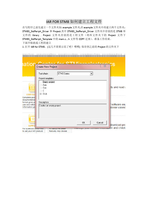
IAR FOR STM8如何建立工程文件
在写程序之前先建立一个文件夹如:example文件夹;在example文件夹中再建立两个文件夹:STM8S_StdPeriph_Driver和Project.其中STM8S_StdPeriph_Driver文件夹中存放的是STM8库文件的library . Project文件夹存放的是工程文件(将库文件夹下的Project文件下STM8S_StdPeriph_Template中的main.c….h文件等COPY过来)。
准备工作结束。
下面开始就成工程的建立
1 .打开IAR for STM8,(这几不需要示范了吧?嘿嘿) 保存到之前的Project的文件夹下
2.在workspace中右键单击example增加Group 两个分别为FW_lib和User.
3.向FW_lib文件夹中添加库文件,库文件在之前建立的STM8S_StdPeriph_Driver文件夹下,添加的是src 文件夹下的,(具体添加哪个你也知道了,不必我多说),
4.向User文件夹下添加文件:Project文件夹下的.c和.h文件
5.此时添加的文件已经完毕,现在需要设置工程的属性了
书写模式如下图所示:
6.最后一步:进行程序的编译,更改程序中的错误。
自此建立工程结束,可以进行Main
函数的书写了。
以上哪有不足之处请多多指教。
嘿嘿!。
IAR FOR STM8例程要点

IAR+STM8——EXTI外部中断控制寄存器2013-03-21 23:23:15| 分类:STM8|举报|字号订阅这块三合一的开发板上有且只有一个按键,没办法,就拿这唯一的按键来用吧。
吸取前面UART3的教训,先看开发板的原理图吧。
这个按键被接到了STM8S207SB的PD7上,已做了上拉处理。
为了简单明了,还是点LED1吧。
按一下LED1亮,再按一下LED1灭。
好了,写程序吧。
#i nclude <iostm8s207sb.h>#define LED1_FLASH PD_ODR_ODR3 = !PD_ODR_ODR3 // 开发板上的LED1接在PD3上void GPIO_init(void){PD_DDR = 0x08; // 配置PD端口的方向寄存器PD3输出PD_CR1 = 0x08; // 设置PD3为推挽输出PD_CR2 = 0x80; // 使能PD7外部中断}void EXTI_init(void){EXTI_CR1 = 0x80; // PD口下降沿触发中断}#pragma vector=0x02 // 这里很关键!看下面说明。
__interrupt void EXTI_PD7_TLI(void){LED1_FLASH;}void init_devices(void){asm("sim"); // 关全局中断GPIO_init();EXTI_init();asm("rim"); // 开全局中断}void main( void ){init_devices();// 主循环里没有程序需要执行while(1);}这里着重要说明的一点是PD7的外部中断程序。
看了一下芯片手册,PD口外部中断EXTI3的中断向量号是6,想当然,又是想当然,按IAR的规矩中断向量要加2,就这样写#pragma vector=0x08,结果就是按下按键,程序没响应了,一直在中断里不出来。
ST单片机STM8S开发入门教程

ST单片机STM8S开发入门教程最近ST在国内大力推广他的8位高性价比单片机STM8S系列,感觉性能上还是非常不错的,网上稍微看了点资料,打算有机会还是学习一下,先入门为以后做好技术积累。
好了,长话短说。
手上拿到一套ST最近做活动赠送的三合一学习套件,上面包括STM32F小板、ST LINK小板、STM8S小板,做工很精致,相信很多朋友也收到了。
既然当初去申请了,人家也送了,总得把用起来吧,放着吃灰尘是很可惜的^_^ 。
好,步入正题,刚开始在论坛上逛了一圈,感觉STM8S的资料实在太少,都是官方的应用资料,没有什么入门介绍,连需要安装什么软件都搞不清楚。
偶的电脑光驱坏了,所以也读不出光盘里有什么东西,所以只能到处瞎摸,还是ourdev论坛好,嘿嘿,仔细看了几个帖子,总算明白大概是什么样的开发环境了。
用C语言开发STM8S,需要安装两个软件:1、STVD IDE开发环境;2、COSMIC for STM8 C编译器。
STVD可以到官网下载,下载地址:COSMIC 需要申请LICENSE,比较繁琐,刚好坛子有人传了一个免安装无限制版本的,偶就赶紧下载了,大家可以去下载,仅做为个人学习使用。
下载地址:软件下载后,只需安装STVD。
从上面地址下载的COSMIC不用安装,只要解压到硬盘即可。
后面建立工程的时候设置好路径即可。
下面一步一步开始啦~一、安装好STVD后,桌面上建立了两个快捷图标,ST Visual Develop就是STVD了。
ST Visual Programmer是编程软件,可以配合ST LINK对STM8S进行编程烧录。
二、双击运行ST Visual Develop,启动STVD开发环境。
执行Workspace,在New Workspace 窗口里选择Create workspace and projects,点击“确定”建立工作组和工程三、在Workspace 里输入Workspace名称,由于最终我们要测试一个现成的LED程序,所以偶写了led,随你喜欢了,呵呵。
- 1、下载文档前请自行甄别文档内容的完整性,平台不提供额外的编辑、内容补充、找答案等附加服务。
- 2、"仅部分预览"的文档,不可在线预览部分如存在完整性等问题,可反馈申请退款(可完整预览的文档不适用该条件!)。
- 3、如文档侵犯您的权益,请联系客服反馈,我们会尽快为您处理(人工客服工作时间:9:00-18:30)。
AN2659Application noteSTM8S in-application programming (IAP)using a customized bootloaderIntroductionThis application note is intended for STM8 firmware and system designers who need toimplement an In-Application Programming (IAP) feature in the product they are developingwith the STM8S microcontroller.The STM8S is an 8-bit microcontroller family with Flash memory for user program code orfirmware.IAP makes it possible to update the firmware ‘in situ’, after the microcontroller has beenembedded in the final product. The advantage is that the microcontroller board can stayinside its product enclosure, no mechanical intervention is needed to do the update.IAP is extremely useful for distributing new firmware versions. It makes it easy to add newproduct features and correct problems throughout the product life cycle.The bootloader firmware source code provided with this application note shows an exampleof how to implement IAP for the STM8 microcontroller. Y ou can use this code as a referencewhen integrating IAP in your STM8 application.February 2009 Rev 11/18Contents AN2659Contents1Theory of operation . . . . . . . . . . . . . . . . . . . . . . . . . . . . . . . . . . . . . . . . . 31.1Block versus word programming . . . . . . . . . . . . . . . . . . . . . . . . . . . . . . . . 31.2RAM versus Flash programming code location . . . . . . . . . . . . . . . . . . . . . 31.2.1Programming the data EEPROM area . . . . . . . . . . . . . . . . . . . . . . . . . . . 41.3Flash memory protection, bootloader . . . . . . . . . . . . . . . . . . . . . . . . . . . . . 41.4Library support for Flash programming . . . . . . . . . . . . . . . . . . . . . . . . . . . 52Library support for IAP . . . . . . . . . . . . . . . . . . . . . . . . . . . . . . . . . . . . . . . 62.1Flash programming function list . . . . . . . . . . . . . . . . . . . . . . . . . . . . . . . . . 63Compiler support (Cosmic) for RAM code execution . . . . . . . . . . . . . . 83.1Description how to compile/link code into RAM address locations . . . . . . 84STM8 devices with boot ROM - built-in IAP implementation . . . . . . . . 104.1Implementation details . . . . . . . . . . . . . . . . . . . . . . . . . . . . . . . . . . . . . . . 104.2Bootloader protocol . . . . . . . . . . . . . . . . . . . . . . . . . . . . . . . . . . . . . . . . . 105Example of user bootloader application . . . . . . . . . . . . . . . . . . . . . . . . 115.1Bootloader firmware description . . . . . . . . . . . . . . . . . . . . . . . . . . . . . . . . 115.2Used library functions . . . . . . . . . . . . . . . . . . . . . . . . . . . . . . . . . . . . . . . . 145.3Block programming - RAM code copy . . . . . . . . . . . . . . . . . . . . . . . . . . . 145.4Interrupt vector table redirection . . . . . . . . . . . . . . . . . . . . . . . . . . . . . . . . 145.5Bootloader overwrite protection . . . . . . . . . . . . . . . . . . . . . . . . . . . . . . . . 145.6Used bootloader interface . . . . . . . . . . . . . . . . . . . . . . . . . . . . . . . . . . . . 146Conclusion . . . . . . . . . . . . . . . . . . . . . . . . . . . . . . . . . . . . . . . . . . . . . . . . 166.1Features in final bootloader application . . . . . . . . . . . . . . . . . . . . . . . . . . 16 7Revision history . . . . . . . . . . . . . . . . . . . . . . . . . . . . . . . . . . . . . . . . . . . 172/18AN2659Theory of operation 3/181 Theory of operationIn practice, IAP (In Application Programming) requires a bootloader implemented in theSTM8 firmware that can communicate with an external master (such as a PC) via a suitablecommunications interface. The new code can be downloaded into the microcontrollerthrough this interface. The microcontroller then programs this code into its Flash memory.The STM8 microcontroller family has IAP support in hardware. The software libraryavailable for the STM8 family contains support for IAP programming. This simplifiesimplementation of IAP in the end-user application.IAP programming can also be used to update the content of the internal Data EEPROMmemory, and the internal RAM memory.Figure 1.Typical bootloader application1.1 Block versus word programmingSTM8 family microcontrollers contain Flash type program memory where firmware canwrite. There are two methods for writing (or erasing) Flash program memory:●Byte/word programming (1 or 4 bytes)–Advantages: offers small area programming, programming is done from Flash –Disadvantages: program stops during programming, programming speed is slow●Block programming (128 bytes - or one Flash block for a given STM8 type)–Advantages: offers large area programming with high speed (large blocks)–Disadvantages: programming routine must run from RAM (need to copyprogramming routine into RAM)1.2 RAM versus Flash programming code locationDepending on the selected programming method (see 1.1: Block versus word programming )the programming code must run from RAM or from Flash memory.If the programming code runs from Flash, then we can use only word/byte programming toprogram the Flash memory. During Flash memory programming, the code cannot accessthe Flash memory (Flash is in programming mode). Therefore program execution from Flashis stopped during programming (for several milliseconds) and then continues. This mode isuseful in cases where only a small part (a few bytes) of Flash memory need to be updatedor when it does not matter that programming is (very) slow.RS232RS232/TTL converter STM8 boardSTM8bootloader enable jumperPCTheory of operation AN26594/18To program a large Flash memory area with optimum speed then we should use block programming mode. Block programming mode can be performed only by code located in RAM. First we must copy the programming code into RAM and then run (jump to) this code. The RAM code then uses block mode to program the Flash. In this mode, programming one block takes the same time as programming one byte/word in byte/word mode. As a result programming speed is very fast and code execution is not stopped (because it is running from RAM). The only disadvantage of this method is the RAM code management:–Copying the executable code to RAM–Storing the RAM code (usually stored in Flash - but can be downloaded from outside)–Allocating RAM space for code–Compiling the code to be able to run from RAM1.2.1 Programmingthedata EEPROM areaIn case of data EEPROM programming, the programming code does not have to beexecuted from RAM. It can be located in Flash program memory, even if block programmingis used. This Read-While-Write (RWW) feature speeds up microcontroller performanceduring IAP. Only the data loading phase must execute from RAM - this is the part of codewhich loads data into the EEPROM buffer. However during the physical programming phase(which takes several milliseconds) the code runs from Flash while the data EEPROMmemory is programmed in the background. Completion of data EEPROM programming isindicated by a flag. An interrupt can be generated when the flag is set.1.3 Flash memory protection, bootloaderTo avoid accidental overwriting of Flash code memory (for example in the case of a firmwarecrash) several levels of write protection are implemented in the STM8 microcontroller family.After an STM8 reset, write access to Flash memory is disabled. To enable it, firmware mustwrite 2 unlock keys in a dedicated register. If the unlock keys are correct (0x56, 0xAE) thenwrite access to Flash memory is enabled and it is possible to program Flash memory usingeither byte/word or block programming mode. If the unlock keys are incorrect, then writeaccess to Flash memory is disabled until the next device reset. After writing to Flashmemory, it is recommended to enable write protection again by clearing a specific bit in theFlash control register (to avoid accidental write).A similar protection mechanism exists for Data EEPROM memory, with a specific unlockregister and unlock keys (0xAE, 0x56).Additional write protection exists for programming code itself, to avoid overwriting criticalcode. It is designed to protect the bootloader code from being overwritten during IAP. TheSTM8 family has a user boot code (UBC) area which is permanently write protected. ThisUBC area starts from the Flash memory start address (0x8000) and its size can be changedby option byte. The boot code area includes the interrupt vector table (0x8000 - 0x8080), soto allow for modification of the vector table via IAP, the main vector table should beredirected to another vector table located in the rewritable application code area. See Figure2. for memory map locations and dependencies.AN2659Theory of operation5/18Figure er boot code area and User application areaMore detailed information about memory map of particular STM8 device type can be foundin STM8 Reference manual and datasheet.1.4 Library support for Flash programmingThe STM8 firmware library, available from , provides developed and verified functionsfor programming Flash memory. Those functions supports byte/word and blockprogramming. These library functions make it easier for developers to write theirprogramming code. The library also includes functions for managing the programming codein RAM: copy to RAM, execution from RAM, storing functions in Flash memory.The STM8 library package also contains examples that show how to use these functions inthe final source code. Y ou can write your own code based on these examples.AddressContent 0x6000ROM code ...0x8000interrupt vector table 0x8080bootloader start .....................bootloader end 0x9000user interrupt table 0x9080user code start .....................user code end ...free space ............r e d i r e c t i o n UBC User application User boot code area defined by option byteareaLibrary support for IAP AN2659 2 Library support for IAPSTM8 library contains modules for Flash programming. These are contained in the followingfiles:\FWLib\library\src\stm8s_flash.c\FWLib\library\inc\stm8s_flash.h\FWLib\library\inc\stm8s_map.hHere you can find the complete source code for Flash programming. Refer to the library usermanual, \FWLib\stm8s_fwlib_um.chm, for help on using STM8 library.2.1 Flash programming function listThis list gives a short description of the STM8S Flash programming functions:void FLASH_DeInit ( void )Deinitializes the FLASH peripheral registers to their default reset values.void FLASH_EraseBlock ( u16 BlockNum, FLASH_MemT ype_T ypeDef MemT ype ) Erases a block in the program or data EEPROM memory.void FLASH_EraseByte ( u32 Address )Erases one byte in the program or data EEPROM memory.void FLASH_EraseOptionByte ( u32 Address )Erases an option byte.u32 FLASH_GetBootSize ( void )Returns the Boot memory size in bytes.FlagStatus FLASH_GetFlagStatus ( FLASH_Flag_T ypeDef FLASH_FLAG )Checks whether the specified Flash flag is set or not.FLASH_LPMode_T ypeDef FLASH_GetLowPowerMode ( void )Returns the Flash behavior type in low power mode.FLASH_ProgramTime_T ypeDef FLASH_GetProgrammingTime ( void )Returns the fixed programming time.void FLASH_ITConfig ( FunctionalState NewState )Enables or Disables the Flash interrupt mode.void FLASH_Lock ( FLASH_MemT ype_T ypeDef MemT ype )Locks the program or data EEPROM memory.void FLASH_ProgramBlock ( u16 BlockNum, FLASH_MemT ype_T ypeDef MemT ype, FLASH_ProgramMode_T ypeDef ProgMode, u8 * Buffer )Programs a memory block.void FLASH_ProgramByte ( u32 Address, u8 Data )Programs one byte in program or data EEPROM memory.void FLASH_ProgramOptionByte ( u32 Address, u8 Data )Programs an option byte.6/18AN2659Library support for IAP void FLASH_ProgramWord ( u32 Address, u32 Data )Programs one word (4 bytes) in program or data EEPROM memory.u8 FLASH_ReadByte ( u32 Address )Reads any byte from Flash memory.u16 FLASH_ReadOptionByte ( u32 Address )Reads one option byte.void FLASH_SetLowPowerMode ( FLASH_LPMode_T ypeDef LPMode )Select the Flash behavior in low power mode.void FLASH_SetProgrammingTime ( FLASH_ProgramTime_T ypeDef ProgTime )Sets the fixed programming time.void FLASH_Unlock ( FLASH_MemT ype_T ypeDef MemT ype )Unlocks the program or data EEPROM memory.FLASH_Status_T ypeDef FLASH_WaitForLastOperation ( FLASH_MemT ype_T ypeDef MemT ype )Wait for a Flash operation to complete.7/183 Compiler support (Cosmic) for RAM code executionAs mentioned above, block programming must be executed from RAM memory. Thereforethe code to be copied into RAM must be compiled and linked to be run in RAM addressspace but stored in Flash memory.It is possible to write simple programming code assembly, taking care with the RAMaddressing and then storing this code in Flash (e.g. code uses only relative addressing orRAM addresses). However it is more efficient to use compiler support for this purpose.Cosmic compiler support (described below) has these features built-in.3.1 Description how to compile/link code into RAM addresslocationsThis option is performed (in Cosmic compiler) by creating a special memory segment whichis defined in the linker file (*.lkf) and marked by flag “-ic” . For example (RAM spacesegments definition in linker file):# Segment Ram:+seg .data -b 0x100 -m 0x500 -n .data+seg .bss -a .data -n .bss+seg .E_W_ROUTs -a .bss -n bootcode -icThis defines a RAM space from address 0x100. Firstly the .data and .bss sections aredefined. Then it defines a moveable .E_W_ROUTs section where the routines for Flashmemory erase and write operations will be located. This section must be marked by option“-ic” (moveable code).Into “-ic” marked section we put functions which should be compiled/linked for RAMexecution but stored in Flash memory. This is done in source code by section definition, forexample:...//set code section to E_W_ROUTs placement#pragma section (E_W_ROUTs)void FlashWrite(void){...}void FlashErase(void){...}//set back code section to default placement#pragma section ()...8/18Now the “FlashWrite()” and “FlashErase()” functions will be compiled and linked for RAM execution (in section “E_W_ROUTs”) but their code will be placed in Flash memory - just after the“.text” and “.init” sections. This can seen from the generated map file:Example of final map file:--------Segments--------start 00008080 end 00008500 length 1152 segment .textstart 00000000 end 00000000 length 0 segment .bsctstart 00000000 end 00000003 length 3 segment .ubsctstart 00000003 end 00000098 length 149 segment .RAMstart 00000098 end 00000098 length 0 segment .sharestart 00000100 end 00000100 length 0 segment .datastart 00000100 end 00000100 length 0 segment .bssstart 00000100 end 000001F0 length 240 segment .E_W_ROUTs, initialized start 00008510 end 00008600 length 240 segment .E_W_ROUTs, fromstart 00008000 end 00008080 length 128 segment .conststart 00008500 end 00008510 length 16 segment .initThe map file shows the location of the “E_W_ROUTs” sections. One for storage in Flash (in map file marked as “from”) and one for execution (in map file marked as “initialized”). Finally the microcontroller firmware must copy these sections from Flash to RAM before calling the RAM functions. Cosmic compiler support this copying by a built-in function “int _fctcpy(char name)” which copies a whole section from a source location in Flash to a destination location in RAM. For example:void main(void){...//copy programming routines to Flash_fctcpy('b');/* Define flash programming Time*/FLASH_SetProgrammingTime(FLASH_PROGRAMTIME_STANDARD);/* Unlock Program & Data memories */FLASH_Unlock(FLASH_MEMTYPE_DATA);FLASH_Unlock(FLASH_MEMTYPE_PROG);/* Fill the buffer in RAM */for (i = 0; i < FLASH_BLOCK_SIZE; i++) GBuffer[i] = new_val2;/* Program the block 0*/block = 0; /*block 0 is first block of Data memory: address is 4000*/FLASH_ProgramBlock(block, FL_MEMTYPE_PROG, FL_PRGMODE_STD, GBuffer); ...}As shown in the example above, just after the program starts, the RAM section is copied from Flash into RAM by the function “_fctcpy('b')”. The function parameter ‘b’ is the first character of the section name defined in the linker file (“b” as “bootcode” - see linker file on page 8) .The firmware then can call any of the FLASH_xxx() functions in RAM.Execution is then done from RAM.9/18STM8 devices with boot ROM - built-in IAP implementation AN265910/18 4 STM8 devices with boot ROM - built-in IAP implementationSome but not all STM8 devices have an internal Boot ROM memory which contains abootloader and thus already have a built in IAP implementation. So the IAP exampledescribed in this application note is primarily intended for STM8 devices that have no BootROM.4.1 Implementation detailsThe built-in bootloader in BootROM is fixed (not rewritable) and is specific for each STM8type. The communication interface supported depends on the peripherals present in thegiven STM8 type and if they are implemented in the bootloader. For example, some devicetypes support firmware download through UART and CAN, some device types support onlyUART and others only SPI. Information concerning the supported interfaces can be found inthe relevant device datasheet.Activation of the built-in bootloader is done by programming the BL[7:0] option bytedescribed in the datasheet. The Boot ROM bootloader checks this option byte and ifenabled then it runs it own code - waits for the host to send commands/data. If the BL[7:0]option byte is inactive then the Boot ROM bootloader jumps to user reset address - 0x8000.4.2 Bootloader protocolTo be able to download firmware into the device, the host and bootloader must communicatethrough the same protocol. This bootloader protocol for STM8 devices is specified in the“UM0560 - Bootloader user manual” available from . This same protocol isused in the firmware example provided with this application note. The UM0560 user manualdescribes all the bootloader protocol properties: used interfaces, timeouts, commandformats, packet formats, error management, ... .5 Example of user bootloader applicationThis section describes a practical application of IAP programming with a user - implementedbootloader.A bootloader is the part of code which runs immediately after a microcontroller reset andwaits for an activation signal (for example from grounding a specific pin or receiving a tokenfrom a communications interface).If activation is successful then the code enters bootloader mode. If activation fails (forexample due to timeout, jumper on pin not present) then the bootloader jumps directly to theuser application code.In bootloader mode, the bootloader communicates with the external master device througha selected interface (UART, SPI, I2C, CAN, ...) using a set of commands. These commandsusually are write to Flash, erase Flash, verify Flash and some additional operations: readmemory, execute code from given address (jump to given address).firmwaredescription5.1 BootloaderThe following flow chart (Figure 3.: Bootloader flowchart) describes the basic program flowof the bootloader application.After device reset, the bootloader checks if it is activated by predefined I/O pin. This pinworks as bootloader activation signal and is connected via a jumper to ground. Thebootloader configures the I/O pin in input mode and activates the pull-up on the I/O port.Then it checks the pin state. If the pin voltage level is zero (jumper present) then bootloaderis activated. Otherwise it jumps to the reset address of the user application (if this address isvalid).If the bootloader is activated it then initializes the communication interface (UART1) inreceiver mode and starts a timeout count (e.g. 1 second). If during this timeout nothing isreceived from UART1 then the bootloader jumps to the user application reset address (ifvalid).If the bootloader a valid activating token byte receives from UART1 before the timeoutelapses, it then enters memory management mode to perform the following operations:1.First the bootloader initializes the Flash programming routines by copying theprogramming functions to RAM.2. Then bootloader waits in a loop for a valid command to be received from UART1.3. If valid command is received it is parsed and executed (Read, Write, Erase, Versioncommands).4. If a Go command is received, then the bootloader jumps to the address given in thecommand (from which can be returned or not depending on the code at the destinationaddress).Commands have given format which is specified and must be followed by both sides:bootloader and master. The command specification handles all possible cases and coverserror management. T o make it easy to meet this specification while performing the morecomplicated operations (for example, fill Flash memory from “*.s19” file), appropriatesoftware with a graphical user interface (GUI) has been written for the master side (usually11/18PC). This GUI can perform all the specified commands. The command specification isincluded with this Application Note as separate document.12/1813/18Figure 3.Bootloader flowchartReset IO pin in GND?Init I/O pin (pull-up)-+User application start Valid user reset vector?+-Received tokenin timeout interval?Perform command-+Wait for command from UARTGO command?(to run user code)+-Jump to GO addressParse commands- WRITE- ERASE- READ- VERSIONInit UARTCopy routines into RAM5.2 Used library functionsThe code available with this application note uses STM8 software library functions byincluding the appropriate files into projects. It uses not only the functions for Flash memoryprogramming management but also the functions for timer management (for example fortimeout counting), UART management (for communications with the master), GPIOmanagement (for configuring the I/O pin), clock management (to set up microcontroller andperipheral speed).The use of the library simplifies the development and makes the main source code simpler.5.3 Block programming - RAM code copyCopying the RAM code from Flash is done with Cosmic compiler support - by the built-infunction “_fctcpy()”. Copying is performed immediately after microcontroller reset - at thebeginning of the “main()” program function.If another compiler is used, this would require a similar alternative solution for building RAMroutines.table redirection5.4 InterruptvectorThe primary interrupt vector table is located in the UBC (User Boot Code) area which iswrite protected. Interrupt table redirection has been implemented to allow the userapplication to change the interrupt vectors.Redirection is performed in the following way. The start of the user application area containsits own interrupt table with the same format as the primary interrupt table, a set of jumps tointerrupt routines (the first table entry is the “user application reset”). The primary interrupttable contains fixed vectors to this user interrupt table. So if an interrupt occurs then it isredirected from the primary interrupt table to the user interrupt table by one jump.The only requirement for the user application is that the user interrupt table must be locatedat a fixed address because the primary interrupt table is not rewritable and jumps to the userinterrupt table at a fixed address). See Figure 2.: User boot code area and User applicationarea for details.5.5 Bootloader overwrite protectionThe bootloader area must be write protected. This protection is done by setting the UBCoption byte according to the bootloader size.The user application area (which begins with the user interrupt vector table) starts in firstunprotected Flash sector after the UBC area.Bootloader protection must be set by SWIM - usually during bootloader programming.5.6 Used bootloader interfaceThe current version of the bootloader code supports UART as communication interface. Infuture versions, other communication interfaces will be supported (SPI, I2C, CAN, LIN). The14/18user application code then can be upgraded via the interface used by the target application (for example, CAN in the case of an automotive system).15/18Conclusion AN2659 6 ConclusionThe STM8 microcontroller has full support for IAP programming. It allows the internal STM8firmware to erase and write to any of its internal memories: Flash program memory, dataEEPROM memory, RAM memory. The short programming times (inherent to the advancedtechnology) can be further decreased by using of fast programming mode (if the destinationmemory is erased). The STM8 RWW (Read While Write) feature allows the microcontrollerto stay at a high performance level even during Flash and/or EEPROM memoryprogramming.The bootloader application presented here, provides designers with an IAP implementationthat they can use to add IAP support into their own final products. The bootloader code isdesigned to run in STM8 family microcontrollers and uses the STM8 software library foreasier programming.6.1 Features in final bootloader application●Bootloader activated by external pin (jumper on PCB)●Interrupt table redirection●Executable RAM code management●Library support for easier programming●Read While Write feature●High level C-language usage●In future: support for multiple communication interfaces16/18AN2659Revision history 17/187 Revision historyTable 1.Document revision history DateRevision Changes20-Feb-20091Initial releaseAN265918/18Please Read Carefully:Information in this document is provided solely in connection with ST products. STMicroelectronics NV and its subsidiaries (“ST”) reserve the right to make changes, corrections, modifications or improvements, to this document, and the products and services described herein at any time, without notice.All ST products are sold pursuant to ST’s terms and conditions of sale.Purchasers are solely responsible for the choice, selection and use of the ST products and services described herein, and ST assumes no liability whatsoever relating to the choice, selection or use of the ST products and services described herein.No license, express or implied, by estoppel or otherwise, to any intellectual property rights is granted under this document. If any part of this document refers to any third party products or services it shall not be deemed a license grant by ST for the use of such third party products or services, or any intellectual property contained therein or considered as a warranty covering the use in any manner whatsoever of such third party products or services or any intellectual property contained therein.UNL ESS OTHERWISE SET FORTH IN ST’S TERMS AND CONDITIONS OF SAL E ST DISCL AIMS ANY EXPRESS OR IMPL IED WARRANTY WITH RESPECT TO THE USE AND/OR SAL E OF ST PRODUCTS INCL UDING WITHOUT L IMITATION IMPL IED WARRANTIES OF MERCHANTABILITY, FITNESS FOR A PARTICULAR PURPOSE (AND THEIR EQUIVALENTS UNDER THE LAWS OF ANY JURISDICTION), OR INFRINGEMENT OF ANY PATENT, COPYRIGHT OR OTHER INTELLECTUAL PROPERTY RIGHT. UNL ESS EXPRESSL Y APPROVED IN WRITING BY AN AUTHORIZED ST REPRESENTATIVE, ST PRODUCTS ARE NOT RECOMMENDED, AUTHORIZED OR WARRANTED FOR USE IN MILITARY, AIR CRAFT, SPACE, LIFE SAVING, OR LIFE SUSTAINING APPLICATIONS, NOR IN PRODUCTS OR SYSTEMS WHERE FAILURE OR MALFUNCTION MAY RESULT IN PERSONAL INJURY, DEATH, OR SEVERE PROPERTY OR ENVIRONMENTAL DAMAGE. ST PRODUCTS WHICH ARE NOT SPECIFIED AS "AUTOMOTIVE GRADE" MAY ONLY BE USED IN AUTOMOTIVE APPLICATIONS AT USER’S OWN RISK.Resale of ST products with provisions different from the statements and/or technical features set forth in this document shall immediately void any warranty granted by ST for the ST product or service described herein and shall not create or extend in any manner whatsoever, any liability of ST.ST and the ST logo are trademarks or registered trademarks of ST in various countries.Information in this document supersedes and replaces all information previously supplied.The ST logo is a registered trademark of STMicroelectronics. All other names are the property of their respective owners.© 2009 STMicroelectronics - All rights reservedSTMicroelectronics group of companiesAustralia - Belgium - Brazil - Canada - China - Czech Republic - Finland - France - Germany - Hong Kong - India - Israel - Italy - Japan - Malaysia - Malta - Morocco - Singapore - Spain - Sweden - Switzerland - United Kingdom - United States of America。