MAX6033AAUT41-T中文资料
MAX4211EEUE+T中文资料

High-Side Power and Current Monitors MAX4210/MAX4211
ABSOLUTE MAXIMUM RATINGS
VCC, IN, CIN1, CIN2 to GND ....................................-0.3V to +6V RS+, RS-, INHIBIT, LE, COUT1, COUT2 to GND ...-0.3V to +30V IOUT, POUT, REF to GND ..........................-0.3V to (VCC + 0.3V) Differential Input Voltage (VRS+ - VRS-) .................................±5V Maximum Current into Any Pin..........................................±10mA Output Short-Circuit Duration to VCC or GND ........................10s Continuous Power Dissipation (TA = +70°C) 6-Pin TDFN (derate 24.4mW/°C above +70°C) ..........1951mW 8-Pin µMAX (derate 4.5mW/°C above +70°C) .............362mW 16-Pin TSSOP (derate 9.4mW/°C above +70°C) ..........754mW 16-Pin Thin QFN (derate 25mW/°C above +70°C) .....2000mW Operating Temperature Range ...........................-40°C to +85°C Junction Temperature ......................................................+150°C Storage Temperature Range .............................-65°C to +150°C Lead Temperature (soldering, 10s) .................................+300°C
MAX6163AESA-T中文资料

General DescriptionThe MAX6161–MAX6168 are precision, low-dropout,micropower voltage references. These three-terminal devices operate with an input voltage range from (V OUT + 200mV) to 12.6V and are available with output volt-age options of 1.25V, 1.8V, 2.048V, 2.5V, 3V, 4.096V,4.5V, and 5V. They feature a proprietary curvature-cor-rection circuit and laser-trimmed thin-film resistors that result in a very low temperature coefficient of 5ppm/°C (max) and an initial accuracy of ±2mV (max).Specifications apply to the extended temperature range (-40°C to +85°C).The MAX6161–MAX6168 typically draw only 100µA of supply current and can source 5mA (4mA for MAX6161) or sink 2mA of load current. Unlike conven-tional shunt-mode (two-terminal) references that waste supply current and require an external resistor, these devices offer a supply current that is virtually indepen-dent of the supply voltage (8µA/V variation) and do not require an external resistor. Additionally, the internally compensated devices do not require an external com-pensation capacitor. Eliminating the external compen-sation capacitor saves valuable board area in space-critical applications. A low-dropout voltage and a supply-independent, ultra-low supply current make these devices ideal for battery-operated, high-perfor-mance, low-voltage systems.The MAX6161–MAX6168 are available in 8-pin SO packages.________________________ApplicationsAnalog-to-Digital Converters (ADCs)Portable Battery-Powered Systems Notebook Computers PDAs, GPS, DMMs Cellular PhonesPrecision +3V/+5V Systems____________________________Features♦±2mV (max) Initial Accuracy♦5ppm/°C (max) Temperature Coefficient ♦5mA Source Current at 0.9mV/mA ♦2mA Sink Current at 2.5mV/mA ♦Stable with 1µF Capacitive Loads ♦No External Capacitor Required ♦100µA (typ) Quiescent Supply Current ♦200mV (max) Dropout at 1mA Load Current ♦Output Voltage Options: 1.25V, 1.8V, 2.048V, 2.5V,3V, 4.096V, 4.5V, 5V19-1650; Rev 3; 8/05MAX6161–MAX6168Precision, Micropower, Low-Dropout, High-Output-Current, SO-8 Voltage References________________________________________________________________Maxim Integrated Products 1___________________Pin Configuration*Insert the code for the desired initial accuracy and temperature coefficient (from the Selector Guide) in the blank to complete the part number.Typical Operating Circuit and Selector Guide appear at end of data sheet.Ordering InformationFor pricing, delivery, and ordering information,please contact Maxim/Dallas Direct!at 1-888-629-4642, or visit Maxim’s website at .M A X 6161–M A X 6168Precision, Micropower, Low-Dropout, High-Output-Current, SO-8 Voltage References 2_______________________________________________________________________________________ABSOLUTE MAXIMUM RATINGSStresses beyond those listed under “Absolute Maximum Ratings” may cause permanent damage to the device. These are stress ratings only, and functional operation of the device at these or any other conditions beyond those indicated in the operational sections of the specifications is not implied. Exposure to absolute maximum rating conditions for extended periods may affect device reliability.Voltages Referenced to GNDIN …………............................................................-0.3 to +13.5V OUT………………........................................-0.3V to (V IN + 0.3V)Output Short-Circuit Duration to GND or IN (V IN ≤6V)...Continuous Output Short-Circuit Duration to GND or IN (V IN > 6V)…...........60sContinuous Power Dissipation (T A = +70°C)8-Pin SO (derate 5.88mW/°C above +70°C)...............471mW Operating Temperature Range ...........................-40°C to +85°C Storage Temperature Range………….…………-65°C to +150°C Lead Temperature (soldering, 10s)……………………….+300°CELECTRICAL CHARACTERISTICS—MAX6161 (V OUT = 1.25V)MAX6161–MAX6168Precision, Micropower, Low-Dropout, High-Output-Current, SO-8 Voltage References_______________________________________________________________________________________3ELECTRICAL CHARACTERISTICS—MAX6168 (V OUT = 1.800V)M A X 6161–M A X 6168Precision, Micropower, Low-Dropout, High-Output-Current, SO-8 Voltage References 4_______________________________________________________________________________________ELECTRICAL CHARACTERISTICS—MAX6162 (V OUT = 2.048V)MAX6161–MAX6168Precision, Micropower, Low-Dropout, High-Output-Current, SO-8 Voltage References_______________________________________________________________________________________5ELECTRICAL CHARACTERISTICS—MAX6166 (V OUT = 2.500V)M A X 6161–M A X 6168Precision, Micropower, Low-Dropout, High-Output-Current, SO-8 Voltage References 6_______________________________________________________________________________________ELECTRICAL CHARACTERISTICS —MAX6163 (V OUT = 3.000V)MAX6161–MAX6168Precision, Micropower, Low-Dropout, High-Output-Current, SO-8 Voltage References_______________________________________________________________________________________7ELECTRICAL CHARACTERISTICS—MAX6164 (V OUT = 4.096V)M A X 6161–M A X 6168Precision, Micropower, Low-Dropout, High-Output-Current, SO-8 Voltage References 8_______________________________________________________________________________________ELECTRICAL CHARACTERISTICS —MAX6167 (V OUT = 4.500V)MAX6161–MAX6168Precision, Micropower, Low-Dropout, High-Output-Current, SO-8 Voltage References_______________________________________________________________________________________9ELECTRICAL CHARACTERISTICS—MAX6165 (V OUT = 5.000V)Note 2:Temperature Coefficient is specified by the “box” method; i.e., the maximum ΔV OUT is divided by the maximum ΔT.Note 3:Thermal Hysteresis is defined as the change in T A = +25°C output voltage before and after temperature cycling of thedevice (from T A = T MIN to T MAX ). Initial measurement at T A = +25°C is followed by temperature cycling the device to T A = +85°C then to T A = -40°C, and another measurement at T A = +25°C is compared to the original measurement at T A = +25°C.Note 4:Dropout voltage is the minimum input voltage at which V OUT changes ≤0.2% from V OUT at V IN = 5.0V (V IN = 5.5V forMAX6165).M A X 6161–M A X 6168Precision, Micropower, Low-Dropout, High-Output-Current, SO-8 Voltage References 10______________________________________________________________________________________Typical Operating Characteristics(V IN = +5V for MAX6161–MAX6168, V IN = +5.5V for MAX6165, I OUT = 0, T A = +25°C, unless otherwise noted.) (Note 5)MAX6161OUTPUT VOLTAGE TEMPERATURE DRIFTTEMPERATURE (°C)O U T P U T V O L T A G E (V )70552540-1010-251.24961.24971.24981.24991.25001.25011.25021.25031.25041.25051.2495-4085MAX6165OUTPUT VOLTAGE TEMPERATURE DRIFTTEMPERATURE (°C)O U T P U T V O L T A G E (V )7055-25-102510404.99854.99904.99955.00005.00055.00105.00155.00204.9980-4085MAX6161LONG-TERM DRIFTM A X 6161/68 t o c 03TIME (hrs)D R I F T (p p m )768192384576-30-20-100102030405060-40960MAX6165LONG-TERM DRIFTM A X 6161/68 t o c 04TIME (hrs)D R I F T (p p m )768192384576-90-80-70-60-50-40-30-20-100-100960-300-200-100010020030024681012MAX6161LINE REGULATIONINPUT VOLTAGE (V)O U T P U T V O L T A G E C H A N G E (μV )-1200-600-800-1000-400-20002005971113MAX6165LINE REGULATIONINPUT VOLTAGE (V)O U T P U T V O L T A G E C H A N G E (μV )-310-1-22345-4-224LOAD CURRENT (mA)O U T P U T V O L T A G E C H A N G E (m V)MAX6161LOAD REGULATION-620-2-44861012-6-2-4246LOAD CURRENT (mA)O U T P U T V O L T A G E C H A N G E (m V )MAX6165LOAD REGULATION0.100.050.200.150.250.30021345MAX6166DROPOUT VOLTAGE vs. LOAD CURRENTLOAD CURRENT (mA)D R O P O U T V O L T A GE (V )MAX6161–MAX6168Output-Current, SO-8 Voltage References______________________________________________________________________________________11Typical Operating Characteristics (continued)(V IN = +5V for MAX6161–MAX6168, V IN = +5.5V for MAX6165, I OUT = 0, T A = +25°C, unless otherwise noted.) (Note 5)00.050.150.100.200.2521345LOAD CURRENT (mA)D R O P O U T V O L T A GE (V )MAX6165DROPOUT VOLTAGE vs. LOAD CURRENTM A X 6161/68 t o c 11FREQUENCY (kHz)P S R R (d B )0-10-20-30-40-50-60-70-80-900.0011101000.010.11000MAX6161POWER-SUPPLY REJECTION RATIOvs. FREQUENCY-70-800.001101000-60-50-40-30-20-100FREQUENCY (kHz)P S R R (d B )0.1MAX6165POWER-SUPPLY REJECTION RATIOvs. FREQUENCYM A X 6161/68 t c 12MAX6161SUPPLY CURRENT vs. SUPPLY VOLTAGESUPPLY VOLTAGE (V)S U P P L Y C U R R E N T (μA )1210864108116124132140148156164172180100214MAX6165SUPPLY CURRENT vs. SUPPLY VOLTAGESUPPLY VOLTAGE (V)S U P P L Y C U R R E N T (μA )1312101178969610210811412012613213814415090514MAX6161SUPPLY CURRENT vs. TEMPERATURETEMPERATURE (°C)S U P P L Y C U R R E N T (μA )603510-15108116124132140148156164172180100-4085MAX6165SUPPLY CURRENT vs. TEMPERATURETEMPERATURE (°C)S U P P L Y C U R R E N T (μA )603510-159610210811412012613213814415090-408500.00110100040206080100140120160180200220M A X 6161/68 t o c 17FREQUENCY (kHz)O U T P U T I M P E D A N C E (Ω)0.1MAX6161OUTPUT IMPEDANCE vs. FREQUENCY1800.00110100040206010080120140160M A X 6161/68 t o c 18FREQUENCY (kHz)O U T P U T I M P E D A N C E (Ω)0.1MAX6165OUTPUT IMPEDANCE vs. FREQUENCYM A X 6161–M A X 6168Output-Current, SO-8 Voltage References 12______________________________________________________________________________________Typical Operating Characteristics (continued)(V IN = +5V for MAX6161–MAX6168, V IN = +5.5V for MAX6165, I OUT = 0, T A = +25°C, unless otherwise noted.) (Note 5)V OUT 10μV/div 1s/div MAX61610.1Hz TO 10Hz OUTPUT NOISEM A X 6161/68 t o c 19V OUT 10μV/div1s/divMAX6165NOISEM A X 6161/68 t o c 20V OUT 500mV/divV IN 5V/div10μs/divMAX6161TURN-ON TRANSIENT(C L = 50pF)M A X 6161/68 t o c 21V OUT 2V/divV IN 5V/div40μs/divMAX6165TURN-ON TRANSIENT(C L = 50pF)M A X 6161/67 t o c 22I OUT 500μA/divV OUTAC-COUPLED 100mV/div400μs/div MAX6161LOAD TRANSIENT(I OUT = ±250μA, V IN = 5.0, C L = 0)+250μA -250μAMAX6161/68 toc23I OUT 500μA/divV OUTAC-COUPLED50mV/div400μs/divMAX6165LOAD TRANSIENT(I OUT = ±250μA, C L = 0, V IN = 5.5V)+250μA -250μAMAX6161/68 toc24MAX6161–MAX6168Output-Current, SO-8 Voltage References______________________________________________________________________________________13I OUT 5mA/divV OUTAC-COUPLED50mV/div400μs/divMAX6165LOAD TRANSIENT(C L = 0, I OUT = ±2mA, V IN = 5.5V)+2mA -2mAMAX6161/68 toc28I OUT 5mA/divV OUTAC-COUPLED 100mV/div 400μs/div MAX6161LOAD TRANSIENT(V IN = 5.0V, C L = 0, I OUT = ±2mA)+2mA-2mAMAX6161/68 toc27I OUT 5mA/divV OUTAC-COUPLED50mV/div400μs/divMAX6161LOAD TRANSIENT(V IN = 5.0V, C L = 1μF, I OUT = ±2mA)+2mA-2mAMAX6161/68 toc29I OUT 5mA/divV OUTAC-COUPLED20mV/div400μs/divMAX6165LOAD TRANSIENT(C L = 1μF, I OUT = ±2mA, V IN = 5.5V)+2mA-2mAMAX6161/68 toc30I OUT 500μA/divV OUTAC-COUPLED10mV/div 400μs/div MAX6161LOAD TRANSIENT(I OUT = ±250μA, V IN = 5.0V, C L = 1μF)+250μA -250μAMAX6161/68 toc25I OUT 500μA/divV OUTAC-COUPLED20mV/div400μs/divMAX6165LOAD TRANSIENT(I OUT = ±250μA, C L = 1μF, V IN = 5.5V)+250μA-250μAMAX6161/68 toc26Typical Operating Characteristics (continued)(V IN = +5V for MAX6161–MAX6168, V IN = +5.5V for MAX6165, I OUT = 0, T A = +25°C, unless otherwise noted.) (Note 5)M A X 6161–M A X 6168Output-Current, SO-8 Voltage References 14______________________________________________________________________________________I OUT 5mA/divV OUTAC-COUPLED50mV/div 400μs/div MAX6161LOAD TRANSIENT(V IN = 5.0V, C L = 1μF, I OUT = ±4mA)+4mA-4mAMAX6161/68 toc33I OUT 5mA/divV OUTAC-COUPLED50mV/div400μs/divMAX6165LOAD TRANSIENT(I OUT = ±5mA, C L = 1μF, V IN = 5.5V)+5mA-5mAMAX6161/68 toc34V IN500mV/divV OUTAC-COUPLED20mV/div 40μs/div MAX6161LINE TRANSIENT(C L = 0)+0.25V-0.25VMAX6161/68 toc35V IN500mV/divV OUTAC-COUPLED20mV/div40μs/divMAX6165LINE TRANSIENT(C L = 0)+0.25V -0.25VMAX6161/68 toc36Note 5:Many of the Typical Operating Characteristics of the MAX6161 family are extremely similar. The extremes of these characteristicsare found in the MAX6161 (1.25V output) and the MAX6165 (5.0V output). The Typical Operating Characteristics of the remain-der of the MAX6161 family typically lie between these two extremes and can be estimated based on their output voltages.Typical Operating Characteristics (continued)(V IN = +5V for MAX6161–MAX6168, V IN = +5.5V for MAX6165, I OUT = 0, T A = +25°C, unless otherwise noted.) (Note 5)I OUT 5mA/divV OUTAC-COUPLED 200mV/div400μs/div MAX6161LOAD TRANSIENT(V IN = 5.0V, C L = 0, I OUT = ±4mA)+4mA-4mAMAX6161/68 toc31I OUT 5mA/divV OUTAC-COUPLED 100mV/div400μs/divMAX6165LOAD TRANSIENT(I OUT = ±5mA, C L = 0, V IN = 5.5V)+5mA-5mAMAX6161/68 toc32MAX6161–MAX6168Output-Current, SO-8 Voltage References______________________________________________________________________________________15Applications InformationInput BypassingF or the best line-transient performance, decouple the input with a 0.1µF ceramic capacitor as shown in the Typical Operating Circuit . Locate the capacitor as close to IN as possible. When transient performance is less important, no capacitor is necessary.Output/Load CapacitanceDevices in the MAX6161 family do not require an output capacitor for frequency stability. In applications where the load or the supply can experience step changes,an output capacitor of at least 0.1µF will reduce the amount of overshoot (undershoot) and improve the cir-cuit’s transient response. Many applications do not require an external capacitor, and the MAX6161 family can offer a significant advantage in applications when board space is critical.Supply CurrentThe quiescent supply current of the series-mode MAX6161 family is typically 100µA and is virtually inde-pendent of the supply voltage, with only an 8µA/V (max) variation with supply voltage. Unlike series refer-ences, shunt-mode references operate with a series resistor connected to the power supply. The quiescent current of a shunt-mode reference is thus a function of the input voltage. Additionally, shunt-mode references have to be biased at the maximum expected load cur-rent, even if the load current is not present at the time.In the MAX6161 family, the load current is drawn from the input voltage only when required, so supply current is not wasted and efficiency is maximized at all input voltages. This improved efficiency reduces power dissi-pation and extends battery life.When the supply voltage is below the minimum speci-fied input voltage (as during turn-on), the devices can draw up to 400µA beyond the nominal supply current.The input voltage source must be capable of providing this current to ensure reliable turn-on.Output Voltage HysteresisOutput voltage hysteresis is the change in the input voltage at T A = +25°C before and after the device is cycled over its entire operating temperature range.Hysteresis is caused by differential package stress appearing across the bandgap core transistors. The typical temperature hysteresis value is 125ppm.Turn-On TimeThese devices typically turn on and settle to within 0.1% of their final value in 50µs to 300µs, depending on the output voltage (see electrical table of part used).The turn-on time can increase up to 1.5ms with the device operating at the minimum dropout voltage and the maximum load.Typical Operating Circuit__________________________Chip Information TRANSISTOR COUNT: 117PROCESS: BiCMOSPin DescriptionPIN NAME FUNCTIONNo Connection. Not internally connected.N.C.1, 3, 5, 7, 82IN Input Voltage GroundGND 46OUTReference OutputM A X 6161–M A X 6168Output-Current, SO-8 Voltage References 16______________________________________________________________________________________Selector GuideMAX6161–MAX6168Maxim cannot assume responsibility f or use of any circuitry other than circuitry entirely embodied in a Maxim product. No circuit patent licenses are implied. Maxim reserves the right to change the circuitry and specifications without notice at any time.Maxim Integrated Products, 120 San Gabriel Drive, Sunnyvale, CA 94086 408-737-7600_____________________17©2005 Maxim Integrated ProductsPrinted USAis a registered trademark of Maxim Integrated Products, Inc.S O I C N .E P SOutput-Current, SO-8 Voltage ReferencesPackage Information(The package drawing(s) in this data sheet may not reflect the most current specifications. For the latest package outline information go to /packages .)。
MAX4173TEUT-T中文资料

Notebook Computers
Portable/Battery-Powered Systems
Smart Battery Packs/Chargers
Cell Phones
Power-Management Systems
General System/Board-Level Current Monitoring
The combination of three gain versions and a userselectable external sense resistor sets the full-scale current reading. This feature offers a high level of integration, resulting in a simple and compact currentsense solution.
+20V/V (MAX4173T) +50V/V (MAX4173F) +100V/V (MAX4173H) ♦ ±0.5% Full-Scale Accuracy ♦ ±0.3mV Input Offset Voltage (MAX4173T) ♦ 420µA Supply Current ♦ Wide 1.7MHz Bandwidth (MAX4173T) ♦ +3V to +28V Operating Supply ♦ Available in Space-Saving SOT23-6 Package
Typical Operating Circuit
0 TO +28V
VSENSE
+3V TO +28V 0.1µF
MAX1722EZK-T中文资料
MAX1722
FB 3
4
OUT
THIN SOT23-5
Pin Configurations are continued at end of data sheet.
________________________________________________________________ Maxim Integrated Products
元器件交易网
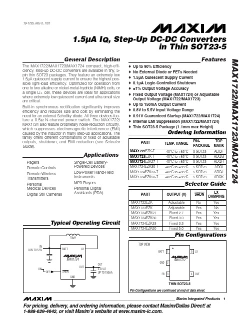
19-1735; Rev 0; 7/01
1.5µA IQ, Step-Up DC-DC Converters in Thin SOT23-5
General Description
The MAX1722/MAX1723/MAX1724 compact, high-efficiency, step-up DC-DC converters are available in tiny, 5pin thin SOT23 packages. They feature an extremely low 1.5µA quiescent supply current to ensure the highest possible light-load efficiency. Optimized for operation from one to two alkaline or nickel-metal-hydride (NiMH) cells, or a single Li+ cell, these devices are ideal for applications where extremely low quiescent current and ultra-small size are critical. Built-in synchronous rectification significantly improves efficiency and reduces size and cost by eliminating the need for an external Schottky diode. All three devices feature a 0.5Ω N-channel power switch. The MAX1722/ MAX1724 also feature proprietary noise-reduction circuitry, which suppresses electromagnetic interference (EMI) caused by the inductor in many step-up applications. The family offers different combinations of fixed or adjustable outputs, shutdown, and EMI reduction (see Selector Guide). o o o o o o o o o o o
ZSPM4013AA1W33中文资料(ZMDI)中文数据手册「EasyDatasheet - 矽搜」

该ZSPM4013采用电流模式反馈 正常调节PWM模式.当稳压 被禁用(EN为低电平)时,设备将小于 10uA静态电流.
该ZSPM4013集成多种防护护电路,包括: 输入欠压锁定,输出电压软启动,限流和热关断.
该ZSPM4013包括通过PG(电源良好)开漏输出 监管报告接口等组成系统.
特征
· 固定输出电压:1.5V,1.8V,2.5V,3.3V, 并用5V +/- 2%输出容差
· ZSPM1000:5A单相,单轨,真 数字PWM控制器(24引脚4×4 QFN)
提供支持
· 评估套件 · 数据表
物理特性
· 结工作温度-40°C至125°C · 包装在一个16针QFN(3×3)
ZSPM4013应用电路
可调输出
ZSPM4013
固定输出 VCC
VOUT
ZSPM4013
EN
PG
芯片中文手册,看全文,戳
2 典型性能特性................................................................................................................... 9 3 电路说明......................................................................................................................................... 12
5 引脚配置和包装......................................................................................................................... 15 5.1.标记图& Pin-out......................................................................................................................... 16 5.2.引脚说明为16引脚3x3 QFN封装....................................................................................................... 17 5.3.详细引脚说明............................................................................................................................. 17 5.3.1.未经稳压输入,VCC(引脚#2,3)....................................... .................................................. ........... 17 5.3.2.引导控制,BST(引脚#10) ......................................................................................................... 17 5.3.3.检测反馈,FB(引脚#5) ............................................................................................................... 17 5.3.4.开关量输出,VSW(引脚#12,13)....................................... .................................................. ......... 18 5.3.5.接地,GND(引脚#4) .......................................................................................................................... 18 5.3.6.电源接地,防护护接地(引脚#14,15)....................................... .................................................. .......... 18 5.3.7.启用,高电压,EN(管脚#9) ........................................................................................................ 18 5.3.8. PG输出,PG(引脚#8) ....................................................................................................................... 18
MAX4313EUA+T中文资料
元器件交易网
MAX4310–MAX4315
High-Speed, Low-Power, Single-Supply Multichannel, Video Multiplexer-Amplifiers
ABSOLUTE MAXIMUM RATINGS
Supply Voltage (VCC to VEE) .................................................12V Input Voltage....................................(VEE - 0.3V) to (VCC + 0.3V) All Other Pins ...................................(VEE - 0.3V) to (VCC + 0.3V) Output Current................................................................±120mA Short-Circuit Duration (VOUT to GND, VCC or VEE)....Continuous Continuous Power Dissipation (TA = +70°C)
________________________________________________________________ Maxim Integrated Products 1
For pricing, delivery, and ordering information, please contact Maxim Direct at 1-888-629-4642, or visit Maxim’s website at .
MAX4211AETE中文资料

4V TO 28V
+ -
+ -
25:1
IOUT POUT
1.21V REFERENCE INHIBIT
REF
CIN1+
COUT1 CIN1LE CIN2+ COUT2
µMAX is a registered trademark of Maxim Integrated Products, Inc. Pin Configurations and Selector Guide appear at end of data sheet.
MAX4211A MAX4211B MAX4211C GND
CIN2-
Functional Diagrams continued at end of data sheet. ________________________________________________________________ Maxim Integrated Products 1
Functional Diagrams
+
VSENSE RSENSE LOAD RS+ VCC 2.7V TO 5.5V RS-
-
Applications
Overpower Circuit Breakers Smart Battery Packs/Chargers Smart Peripheral Control Short-Circuit Protection Power-Supply Displays Measurement Instrumentation Baseband Analog Multipliers VGA Circuits Power-Level Detectors
MAX4230AUK+T,MAX4230AXK+T,MAX4230AXK+T,MAX4230AXK+T,MAX4231AXT+T,MAX4231AXT+T, 规格书,Datasheet 资料
General DescriptionThe MAX4230–MAX4234 single/dual/quad, high-output-drive CMOS op amps feature 200mA of peak output current, rail-to-rail input, and output capability from a single 2.7V to 5.5V supply. These amplifiers exhibit a high slew rate of 10V/µs and a gain-bandwidth product (GBWP) of 10MHz. The MAX4230–MAX4234 can drive typical headset levels (32Ω), as well as bias an RF power amplifier (PA) in wireless handset applications.The MAX4230 comes in a tiny 5-pin SC70 package and the MAX4231, single with shutdown, is offered in a 6-pin SC70 package and in 1.5mm x 1.0mm UCSP and thin µDFN packages. The dual op-amp MAX4233is offered in the space-saving 10-bump chip-scale pack-age (UCSP™), providing the smallest footprint area for a dual op amp with shutdown.These op amps are designed to be part of the PA con-trol circuitry, biasing RF PAs in wireless headsets. The MAX4231/MAX4233 offer a SHDN feature that drives the output low. This ensures that the RF PA is fully dis-abled when needed, preventing unconverted signals to the RF antenna.The MAX4230 family offers low offsets, wide bandwidth,and high-output drive in a tiny 2.1mm x 2.0mm space-saving SC70 package. These parts are offered over the automotive temperature range (-40°C to +125°C).ApplicationsRF PA Biasing Controls in Handset Applications Portable/Battery-Powered Audio Applications Portable Headphone Speaker Drivers (32Ω)Audio Hands-Free Car Phones (Kits)Laptop/Notebook Computers/TFT Panels Sound Ports/Cards Set-Top BoxesDigital-to-Analog Converter Buffers Transformer/Line Drivers Motor DriversFeatureso 200mA Output Drive Capability o Rail-to-Rail Input and Outputo 1.1mA Supply Current per Amplifier o 2.7V to 5.5V Single-Supply Operation o 10MHz Gain-Bandwidth Product o High Slew Rate: 10V/µso 100dB Voltage Gain (R L = 100k Ω)o 85dB Power-Supply Rejection Ratioo No Phase Reversal for Overdriven Inputso Unity-Gain Stable for Capacitive Loads to 780pF oLow-Power Shutdown Mode Reduces Supply Current to < 1µAo Available in 5-Pin SC70 Package (MAX4230)and 6-Pin, UCSP and Thin µDFN Packages (MAX4231)o Available in 10-Bump UCSP Package (MAX4233)MAX4230–MAX4234High-Output-Drive, 10MHz, 10V/µs,Rail-to-Rail I/O Op Amps with Shutdown in SC70________________________________________________________________Maxim Integrated Products 119-2164; Rev 15; 3/12Selector Guide appears at end of data sheet.Pin Configurations appear at end of data sheet.UCSP is a trademark of Maxim Integrated Products, Inc.Ordering InformationTypical Operating CircuitFor pricing, delivery, and ordering information, please contact Maxim Direct at 1-888-629-4642,M A X 4230–M A X 4234High-Output-Drive, 10MHz, 10V/µs,Rail-to-Rail I/O Op Amps with Shutdown in SC70ABSOLUTE MAXIMUM RATINGSStresses beyond those listed under “Absolute Maximum Ratings” may cause permanent damage to the device. These are stress ratings only, and functional operation of the device at these or any other conditions beyond those indicated in the operational sections of the specifications is not implied. Exposure to absolute maximum rating conditions for extended periods may affect device reliability.Supply Voltage (V DD to V SS )....................................................6V All Other Pins...................................(V SS - 0.3V) to (V DD + 0.3V)Output Short-Circuit Duration to V DD or V SS (Note 1)................10s Continuous Power Dissipation (Multilayer, T A = +70°C)5-Pin SC70 (derate 3.1mW/°C above +70°C)..............247mW 5-Pin SOT23 (derate 3.9mW/°C above +70°C)............313mW 6-Pin SC70 (derate 3.1mW/°C above +70°C)..............245mW 6-Pin SOT23 (derate 13.4mW/°C above +70°C)........1072mW 6-Pin Thin µDFN (derate 2.1mW/°C above +70°C)...170.2mW 6-Bump UCSP (derate 3.9mW/°C above +70°C).....308.3mW 8-Pin SOT23 (derate 5.1mW/°C above +70°C).........408.2mW 8-Pin µMAX ®(derate 4.8mW/°C above +70°C) .......387.8mW 10-Pin µMAX (derate 8.8mW/°C above +70°C) .......707.3mW 10-Bump UCSP (derate 5.6mW/°C above +70°C) .....448.7mW 14-Pin SO (derate 11.9mW/°C above +70°C) ..........952.4mW 14-Pin TSSOP (derate 10mW/°C above +70°C) ......796.8mW Operating Temperature Range .........................-40°C to +125°C Junction Temperature......................................................+150°C Storage Temperature Range.............................-65°C to +150°C Lead Temperature(excluding 6 and 10 UCSP, soldering, 10s)................+300°C Soldering Temperature (reflow).......................................+260°CNote 1:Package power dissipation should also be observed.DC ELECTRICAL CHARACTERISTICSµMAX is a registered trademark of Maxim Integrated Products, Inc.MAX4230–MAX4234High-Output-Drive, 10MHz, 10V/µs,Rail-to-Rail I/O Op Amps with Shutdown in SC70_______________________________________________________________________________________3DC ELECTRICAL CHARACTERISTICS (continued)(V DD = 2.7V, V SS = 0V, V CM = V DD /2, V OUT = (V DD /2), R L = ∞connected to (V DD /2), V SHDN = V DD , T A = +25°C , unless otherwise noted.) (Note 2)DC ELECTRICAL CHARACTERISTICS(V DD = 2.7V, V SS = 0V, V CM = V DD /2, V OUT = (V DD /2), R L = ∞connected to (V DD /2), V SHDN = V DD , T A = -40 to +125°C , unless other-M A X 4230–M A X 4234High-Output-Drive, 10MHz, 10V/µs,Rail-to-Rail I/O Op Amps with Shutdown in SC704_______________________________________________________________________________________Note 3:SHDN logic parameters are for the MAX4231/MAX4233 only.Note 4:Guaranteed by design.DC ELECTRICAL CHARACTERISTICS (continued)AC ELECTRICAL CHARACTERISTICS(V = 2.7V, V = 0V, V = V /2, V = (V /2), R = ∞connected to (V /2), V = V , T = +25°C , unless otherwise noted.)MAX4230–MAX4234High-Output-Drive, 10MHz, 10V/µs,Rail-to-Rail I/O Op Amps with Shutdown in SC70_______________________________________________________________________________________5GAIN AND PHASE vs. FREQUENCYFREQUENCY (Hz)0.01k 10k100k1M10M 0.1k 1k100MG A I N (d B )70-30-20-100102030605040P H A S E (D E G R E E S )120-90-60-300906030GAIN AND PHASE vs. FREQUENCY(C L = 250pF)FREQUENCY (Hz)0.01k 10k100k1M10M 0.1k 1k100MG A I N (d B )70-30-20-100102030605040-180P H A S E (D E G R E E S )120-150-120-90-60-30090603000.40.20.80.61.21.01.41.81.62.0-4002040-206080100120SUPPLY CURRENT vs. TEMPERATUREM A X 4230 t o c 05TEMPERATURE (°C)S U P P L Y C U R R E N T (m A )POWER-SUPPLY REJECTION RATIOvs. FREQUENCYFREQUENCY (Hz)0.01k10k100k1M0.1k1k10MP S R R (d B )0-100-90-80-70-60-50-40-10-20-3010001001010.10.011k100k 1M10k10MOUTPUT IMPEDANCE vs. FREQUENCYFREQUENCY (Hz)O U T P U T I M P E D A N C E (Ω)5060708090100110-400-2020406080100120TEMPERATURE (°C)S U P P L Y C U R R E N T (n A )SUPPLY CURRENT vs. TEMPERATURE(SHDN = LOW)__________________________________________Typical Operating Characteristics(V DD = 2.7V, V SS = 0V, V CM = V DD /2, V OUT = V DD /2, R L = ∞, connected to V DD /2, V SHDN = V DD , T A = +25°C, unless otherwise noted.)M A X 4230–M A X 4234High-Output-Drive, 10MHz, 10V/µs,Rail-to-Rail I/O Op Amps with Shutdown in SC706_______________________________________________________________________________________00.60.40.21.00.81.81.61.41.22.02.02.53.03.54.04.55.05.5M A X 4230 t o c 07SUPPLY VOLTAGE (V)S U P P L Y C U R R E N T (m A )SUPPLY CURRENT PER AMPLIFIERvs. SUPPLY VOLTAGE-40-2020406080100120TEMPERATURE (°C)-2-1012V O S (m V )INPUT OFFSET VOLTAGE vs. TEMPERATURE020406080100-400-2020406080100120OUTPUT SWING HIGH vs. TEMPERATURETEMPERATURE (°C)V D D - V O U T (m V )040208060120100140-40020-20406080100120OUTPUT SWING LOW vs. TEMPERATURETEMPERATURE (°C)V O U T - V S S (m V )0.20.80.60.41.01.21.42.01.50.5 1.0 2.53.0 3.54.0 4.55.0SUPPLY CURRENT PER AMPLIFIER vs. COMMON-MODE VOLTAGECOMMON-MODE VOLTAGE (V)S U P P L Y C U R R E N T (m A )-2.0-1.0-1.5-0.50.501.000.51.01.52.02.5INPUT OFFSET VOLTAGE vs. COMMON-MODE VOLTAGEM A X 4230/3 t o c 11COMMON-MODE VOLTAGE (V)I N P U T O F F S E T V O L T A G E (m V )0.20.60.41.00.81.20.51.01.52.02.5SUPPLY CURRENT PER AMPLIFIER vs. COMMON-MODE VOLTAGECOMMON-MODE VOLTAGE (V)S U P P L Y C U R R E N T (m A )0.45101001k10k100kTOTAL HARMONIC DISTORTION PLUS NOISE vs. FREQUENCY0.05FREQUENCY (Hz)T H D +N (%)0.150.250.350.300.200.1000.40TOTAL HARMONIC DISTORTION PLUS NOISE vs. PEAK-TO-PEAK OUTPUT VOLTAGEPEAK-TO-PEAK OUTPUT VOLTAGE (V)T H D +N (%)100.00014.04.24.65.00.0010.11 4.44.8____________________________Typical Operating Characteristics (continued)(V DD = 2.7V, V SS = 0V, V CM = V DD /2, V OUT = V DD /2, R L = ∞, connected to V DD /2, V SHDN = V DD , T A = +25°C, unless otherwise noted.)MAX4230–MAX4234High-Output-Drive, 10MHz, 10V/µs,Rail-to-Rail I/O Op Amps with Shutdown in SC70_______________________________________________________________________________________7400ns/div SMALL-SIGNAL TRANSIENT RESPONSE (NONINVERTING)IN50mV/divMAX4230/34 toc16OUT400ns/div SMALL-SIGNAL TRANSIENT RESPONSE (INVERTING)IN50mV/divMAX4230/34 toc17OUT400ns/divLARGE-SIGNAL TRANSIENT RESPONSE (NONINVERTING)IN1V/div MAX4230/34 toc18OUT400ns/divLARGE-SIGNAL TRANSIENT RESPONSE (INVERTING)IN1V/divMAX4230/34 toc19OUT0501501002002502.03.02.53.54.04.55.0OUTPUT CURRENT vs. OUTPUT VOLTAGE(SOURCING, V DD = 5.0V)OUTPUT VOLTAGE (V)O U T P U T C U R R E N T (m A )20103060705040801.0 1.4 1.6 1.82.01.2 2.2 2.4 2.6 2.83.0OUTPUT CURRENT vs. OUTPUT VOLTAGE(SOURCING, V DD = 2.7V)OUTPUT VOLTAGE (V)O U T P U T C U R R E N T (m A )-80-60-70-40-50-30-20-10000.40.60.20.8 1.0 1.2 1.4 1.6OUTPUT CURRENT vs. OUTPUT VOLTAGE(SINKING, V DD = 2.7V)OUTPUT VOLTAGE (V)O U T P U T C U R R E N T (m A )-250-200-100-150-5001.00.51.52.02.53.0OUTPUT CURRENT vs. OUTPUT VOLTAGE(SINKING, V DD= 5.0V)OUTPUT VOLTAGE (V)O U T P U T C U R R E N T (m A )2001001010010k 100kFREQUENCY (Hz)I N P U T V O L T A G E N O I S E (n V /√H z )1k INPUT VOLTAGE NOISE vs. FREQUENCYM A X 4230/34 t o c 24____________________________Typical Operating Characteristics (continued)(V DD = 2.7V, V SS = 0V, V CM = V DD /2, V OUT = V DD /2, R L = ∞, connected to V DD /2, V SHDN = V DD , T A = +25°C, unless otherwise noted.)M A X 4230–M A X 4234Detailed DescriptionRail-to-Rail Input StageThe MAX4230–MAX4234 CMOS operational amplifiershave parallel-connected n- and p-channel differential input stages that combine to accept a common-mode range extending to both supply rails. The n-channel stage is active for common-mode input voltages typi-cally greater than (V SS + 1.2V), and the p-channel stage is active for common-mode input voltages typi-cally less than (V DD - 1.2V).Applications InformationPackage Power DissipationWarning: Due to the high output current drive, this op amp can exceed the absolute maximum power-dissi-pation rating.As a general rule, as long as the peak cur-rent is less than or equal to 40mA, the maximum package power dissipation is not exceeded for any of the packagetypes offered. There are some exceptions to this rule,however. The absolute maximum power-dissipation rating of each package should always be verified using the fol-lowing equations. The equation below gives an approxi-mation of the package power dissipation:where:V RMS = RMS voltage from V DD to V OUT when sourcing current and RMS voltage from V OUT to V SS when sink-ing current.I RMS = RMS current flowing out of or into the op amp and the load.θ= phase difference between the voltage and the cur-rent. For resistive loads, COS θ= 1.P V I COS IC DISS RMS RMS ()≅θHigh-Output-Drive, 10MHz, 10V/µs,Rail-to-Rail I/O Op Amps with Shutdown in SC708_______________________________________________________________________________________For example, the circuit in Figure 1 has a package power dissipation of 196mW:where:V DC= the DC component of the output voltage.I DC= the DC component of the output current.V PEAK= the highest positive excursion of the AC com-ponent of the output voltage.I PEAK= the highest positive excursion of the AC com-ponent of the output current.Therefore:P IC(DISS)= V RMS I RMS COS θ= 196mWAdding a coupling capacitor improves the package power dissipation because there is no DC current to the load, as shown in Figure 2:Therefore:P IC(DISS)= V RMS I RMS COS θ= 15.6mWIf the configuration in Figure 1 were used with all four of the MAX4234 amplifiers, the absolute maximum power-dissipation rating of this package would be exceeded (see the Absolute Maximum Ratings section).60mW Single-Supply StereoHeadphone Driver Two MAX4230/MAX4231s can be used as a single-sup-ply, stereo headphone driver. The circuit shown in Figure 2 can deliver 60mW per channel with 1% distor-tion from a single 5V supply.The input capacitor (C IN), in conjunction with R IN, forms a highpass filter that removes the DC bias from the incoming signal. The -3dB point of the highpass filter isgiven by:MAX4230–MAX4234High-Output-Drive, 10MHz, 10V/µs, Rail-to-Rail I/O Op Amps with Shutdown in SC70_______________________________________________________________________________________9Figure 2. Circuit Example: Adding a Coupling CapacitorGreatly Reduces Power Dissipation of its PackageFigure 1. MAX4230/MAX4231 Used in Single-Supply OperationCircuit ExampleM A X 4230–M A X 4234Choose gain-setting resistors R IN and R F according to the amount of desired gain, keeping in mind the maxi-mum output amplitude. The output coupling capacitor,C OUT , blocks the DC component of the amplifier out-put, preventing DC current flowing to the load. The out-put capacitor and the load impedance form a highpass filer with the -3dB point determined by:For a 32Ωload, a 100µF aluminum electrolytic capaci-tor gives a low-frequency pole at 50Hz.Bridge AmplifierThe circuit shown in Figure 3 uses a dual MAX4230 to implement a 3V, 200mW amplifier suitable for use in size-constrained applications. This configuration elimi-nates the need for the large coupling capacitor required by the single op-amp speaker driver when sin-gle-supply operation is necessary. Voltage gain is set to 10V/V; however, it can be changed by adjusting the 82k Ωresistor value.Rail-to-Rail Input StageThe MAX4230–MAX4234 CMOS op amps have parallel-connected n- and p-channel differential input stages that combine to accept a common-mode range extend-ing to both supply rails. The n-channel stage is active for common-mode input voltages typically greater than (V SS + 1.2V), and the p-channel stage is active for common-mode input voltages typically less than (V DD -1.2V).Rail-to-Rail Output StageThe minimum output is within millivolts of ground for sin-gle-supply operation, where the load is referenced to ground (V SS ). Figure 4 shows the input voltage range and the output voltage swing of a MAX4230 connected as a voltage follower. The maximum output voltage swing is load dependent; however, it is guaranteed to be within 500mV of the positive rail (V DD = 2.7V) even with maximum load (32Ωto ground).Observe the Absolute Maximum Ratings for power dis-sipation and output short-circuit duration (10s, max)because the output current can exceed 200mA (see the Typical Operating Characteristics .)Input CapacitanceOne consequence of the parallel-connected differential input stages for rail-to-rail operation is a relatively large input capacitance C IN (5pF typ). This introduces a pole at frequency (2πR ′C IN )-1, where R ′is the parallel combi-nation of the gain-setting resistors for the inverting or noninverting amplifier configuration (Figure 5). If the pole frequency is less than or comparable to the unity-gain bandwidth (10MHz), the phase margin is reduced, and the amplifier exhibits degraded AC performance through either ringing in the step response or sustained oscilla-tions. The pole frequency is 10MHz when R ′= 2k Ω. To maximize stability, R ′<< 2k Ωis recommended.High-Output-Drive, 10MHz, 10V/µs,Rail-to-Rail I/O Op Amps with Shutdown in SC7010______________________________________________________________________________________Figure 4. Rail-to-Rail Input/Output RangeFigure 3. Dual MAX4230/MAX4231 Bridge Amplifier for 200mW at 3VIN 1V/divOUT 1V/div5µs/divV CC = 3.0V R L = 100k ΩTo improve step response when R ′> 2k Ω, connect small capacitor C f between the inverting input and out-put. Choose C f as follows:C f = 8(R / R f ) [pf]where R f is the feedback resistor and R is the gain-set-ting resistor (Figure 5).Driving Capacitive LoadsThe MAX4230–MAX4234 have a high tolerance for capacitive loads. They are stable with capacitive loads up to 780pF. Figure 6 is a graph of the stable operating region for various capacitive loads vs. resistive loads.Figures 7 and 8 show the transient response with excessive capacitive loads (1500pF), with and without the addition of an isolation resistor in series with the output. Figure 9 shows a typical noninverting capaci-tive-load-driving circuit in the unity-gain configuration.MAX4230–MAX4234Rail-to-Rail I/O Op Amps with Shutdown in SC70Figure 5. Inverting and Noninverting Amplifiers with Feedback CompensationFigure 6. Capacitive-Load Stability1µs/divV DD = 3.0V, C L = 1500pF R L = 100k Ω, R ISO = 39ΩFigure 8. Small-Signal Transient Response with Excessive Capacitive Load with Isolation Resistor1µs/divV DD = 3.0V, C L = 1500pF R L = 100k Ω, R ISO = 0ΩFigure 7. Small-Signal Transient Response with Excessive Capacitive LoadM A X 4230–M A X 4234The resistor improves the circuit’s phase margin by iso-lating the load capacitor from the op amp’s output.Power-Up and Shutdown ModesThe MAX4231/MAX4233 have a shutdown option. When the shutdown pin (SHDN ) is pulled low, supply current drops to 0.5µA per amplifier (V DD = 2.7V), the ampli-fiers are disabled, and their outputs are driven to V SS .Since the outputs are actively driven to V SS in shut-down, any pullup resistor on the output causes a cur-rent drain from the supply. Pulling SHDN high enables the amplifier. In the dual MAX4233, the two amplifiers shut down independently. Figure 10 shows the MAX4231’s output voltage to a shutdown pulse. The MAX4231–MAX4234 typically settle within 5µs after power-up. Figures 11 and 12 show I DD to a shutdown plus and voltage power-up cycle.When exiting shutdown, there is a 6µs delay before the amplifier’s output becomes active (Figure 10).Rail-to-Rail I/O Op Amps with Shutdown in SC70Figure 9. Capacitive-Load-Driving Circuit 100µs/divFigure 11. Shutdown Enable/Disable Supply Current40µs/divFigure 12. Power-Up/Down Supply Current4µs/divFigure 10. Shutdown Output Voltage Enable/Disable Selector GuideAMPS PER PACKAGE SHUTDOWN Single Single Dual Dual QuadMAX4230–MAX4234Rail-to-Rail I/O Op Amps with Shutdown in SC70Pin ConfigurationsPower Supplies and LayoutThe MAX4230–MAX4234 can operate from a single 2.7V to 5.5V supply, or from dual ±1.35V to ±2.5V sup-plies. For single-supply operation, bypass the power supply with a 0.1µF ceramic capacitor. For dual-supply operation, bypass each supply to ground. Good layout improves performance by decreasing the amount of stray capacitance at the op amps’ inputs and outputs.Decrease stray capacitance by placing external com-ponents close to the op amps’ pins, minimizing trace and lead lengths.Ordering Information (continued)M A X 4230–M A X 4234Rail-to-Rail I/O Op Amps with Shutdown in SC70Package InformationFor the latest package outline information and land patterns, go to /packages . Note that a “+”, “#”, or “-” in the package code indicates RoHS status only. Package drawings may show a different suffix character, but the drawing pertains to the package regardless of RoHS status.MAX4230–MAX4234Rail-to-Rail I/O Op Amps with Shutdown in SC70Package Information (continued)For the latest package outline information and land patterns, go to /packages . Note that a “+”, “#”, or “-” in the package code indicates RoHS status only. Package drawings may show a different suffix character, but the drawing pertains to the package regardless of RoHS status.M A X 4230–M A X 4234Rail-to-Rail I/O Op Amps with Shutdown in SC70Package Information (continued)For the latest package outline information and land patterns, go to /packages . Note that a “+”, “#”, or “-” in the package code indicates RoHS status only. Package drawings may show a different suffix character, but the drawing pertains to the package regardless of RoHS status.MAX4230–MAX4234Rail-to-Rail I/O Op Amps with Shutdown in SC70Package Information (continued)For the latest package outline information and land patterns, go to /packages . Note that a “+”, “#”, or “-” in the package code indicates RoHS status only. Package drawings may show a different suffix character, but the drawing pertains to the package regardless of RoHS status.M A X 4230–M A X 4234Rail-to-Rail I/O Op Amps with Shutdown in SC70Package Information (continued)For the latest package outline information and land patterns, go to /packages . Note that a “+”, “#”, or “-” in the package code indicates RoHS status only. Package drawings may show a different suffix character, but the drawing pertains to the package regardless of RoHS status.MAX4230–MAX4234Rail-to-Rail I/O Op Amps with Shutdown in SC70Package Information (continued)For the latest package outline information and land patterns, go to /packages . Note that a “+”, “#”, or “-” in the package code indicates RoHS status only. Package drawings may show a different suffix character, but the drawing pertains to the package regardless of RoHS status.M A X 4230–M A X 4234Rail-to-Rail I/O Op Amps with Shutdown in SC70Package Information (continued)For the latest package outline information and land patterns, go to /packages . Note that a “+”, “#”, or “-” in the package code indicates RoHS status only. Package drawings may show a different suffix character, but the drawing pertains to the package regardless of RoHS status.MAX4230–MAX4234Rail-to-Rail I/O Op Amps with Shutdown in SC70______________________________________________________________________________________21Package Information (continued)For the latest package outline information and land patterns, go to /packages . Note that a “+”, “#”, or “-” in the package code indicates RoHS status only. Package drawings may show a different suffix character, but the drawing pertains to the package regardless of RoHS status.M A X 4230–M A X 4234Rail-to-Rail I/O Op Amps with Shutdown in SC7022______________________________________________________________________________________Package Information (continued)For the latest package outline information and land patterns, go to /packages . Note that a “+”, “#”, or “-” in the package code indicates RoHS status only. Package drawings may show a different suffix character, but the drawing pertains to the package regardless of RoHS status.MAX4230–MAX4234Rail-to-Rail I/O Op Amps with Shutdown in SC70______________________________________________________________________________________23Package Information (continued)For the latest package outline information and land patterns, go to /packages . Note that a “+”, “#”, or “-” in the package code indicates RoHS status only. Package drawings may show a different suffix character, but the drawing pertains to the package regardless of RoHS status.M A X 4230–M A X 4234Rail-to-Rail I/O Op Amps with Shutdown in SC7024______________________________________________________________________________________Package Information (continued)For the latest package outline information and land patterns, go to /packages . Note that a “+”, “#”, or “-” in the package code indicates RoHS status only. Package drawings may show a different suffix character, but the drawing pertains to thepackage regardless of RoHS status.MAX4230–MAX4234Rail-to-Rail I/O Op Amps with Shutdown in SC70______________________________________________________________________________________25Package Information (continued)For the latest package outline information and land patterns, go to /packages . Note that a “+”, “#”, or “-” in the package code indicates RoHS status only. Package drawings may show a different suffix character, but the drawing pertains to thepackage regardless of RoHS status.M A X 4230–M A X 4234Rail-to-Rail I/O Op Amps with Shutdown in SC7026______________________________________________________________________________________Package Information (continued)For the latest package outline information and land patterns, go to /packages . Note that a “+”, “#”, or “-” in the package code indicates RoHS status only. Package drawings may show a different suffix character, but the drawing pertains to the package regardless of RoHS status.MAX4230–MAX4234Rail-to-Rail I/O Op Amps with Shutdown in SC70______________________________________________________________________________________27Package Information (continued)For the latest package outline information and land patterns, go to /packages . Note that a “+”, “#”, or “-” in the package code indicates RoHS status only. Package drawings may show a different suffix character, but the drawing pertains to the package regardless of RoHS status.M A X 4230–M A X 4234Rail-to-Rail I/O Op Amps with Shutdown in SC70Maxim cannot assume responsibility for use of any circuitry other than circuitry entirely embodied in a Maxim product. No circuit patent licenses are implied. Maxim reserves the right to change the circuitry and specifications without notice at any time. The parametric values (min and max limits) shown in the Electrical Characteristics table are guaranteed. Other parametric values quoted in this data sheet are provided for guidance.28____________________Maxim Integrated Products, 120 San Gabriel Drive, Sunnyvale, CA 94086 408-737-7600©2012 Maxim Integrated ProductsMaxim is a registered trademark of Maxim Integrated Products, Inc.Revision History。
- 1、下载文档前请自行甄别文档内容的完整性,平台不提供额外的编辑、内容补充、找答案等附加服务。
- 2、"仅部分预览"的文档,不可在线预览部分如存在完整性等问题,可反馈申请退款(可完整预览的文档不适用该条件!)。
- 3、如文档侵犯您的权益,请联系客服反馈,我们会尽快为您处理(人工客服工作时间:9:00-18:30)。
General DescriptionThe MAX6033 ultra-high-precision series voltage refer-ence features a low 7ppm/°C (max) temperature coeffi-cient and a low dropout voltage (200mV, max). Low temperature drift and low noise make the MAX6033ideal for use with high-resolution ADCs or DACs.This device uses bandgap technology for low-noise per-formance and excellent accuracy. Laser-trimmed, high-stability, thin-film resistors, and postpackage trimming guarantee excellent initial accuracy (±0.04%, max). The MAX6033 consumes only 40µA of supply current and sources up to 15mA. Series mode references save sys-tem power and use minimal external components com-pared to two-terminal shunt references.The MAX6033 is available in the miniature 6-pin SOT23package and is offered over the automotive tempera-ture range (-40°C to +125°C).ApplicationsPrecision Regulators A/D and D/A Converters Power Supplies Hard-Disk DrivesHigh-Accuracy Industrial and Process Control Hand-Held InstrumentsFeatureso Tiny 6-Pin SOT23 Packageo Ultra-Low Temperature Drift: 7ppm/°C (max)o ±0.04% Initial Accuracy o Stable with Capacitive Loadso Low 16µV P-P Noise (0.1Hz to 10Hz) (2.5V Output)o 15mA Output Source Current o Low 200mV Dropout Voltage o Low 40µA Quiescent Current o Wide 2.7V to 12.6V Supply Voltage o Excellent Load Regulation: 0.001mV/mAMAX6033Ultra-High-Precision SOT23 SeriesVoltage Reference________________________________________________________________Maxim Integrated Products 1Selector GuidePin ConfigurationOrdering InformationTypical Operating Circuit19-2300; Rev 2; 6/03For pricing, delivery, and ordering information,please contact Maxim/Dallas Direct!at 1-888-629-4642, or visit Maxim’s website at .Note:Two-number part suffix indicates output voltage option.SOT23 Package Top Marks appear at end of data sheet.M A X 6033Ultra-High-Precision SOT23 Series Voltage ReferenceABSOLUTE MAXIMUM RATINGSELECTRICAL CHARACTERISTICS —V OUT = 2.500V(V IN = 5V, C OUT = 0.1µF, I OUT = 0, T A = T MIN to T MAX , unless otherwise specified. Typical values are at T A = +25°C.) (Note 1)Stresses beyond those listed under “Absolute Maximum Ratings” may cause permanent damage to the device. These are stress ratings only, and functional operation of the device at these or any other conditions beyond those indicated in the operational sections of the specifications is not implied. Exposure to absolute maximum rating conditions for extended periods may affect device reliability.IN to GND...............................................................-0.3V to +13V OUTF, OUTS to GND................................................-0.3V to +6V Continuous Power Dissipation (T A = +70°C)6-Pin SOT23 (derate 9.1mW/°C above +70°C)............727mWOperating Temperature Range .........................-40°C to +125°C Storage Temperature Range.............................-65°C to +150°C Maximum Junction Temperature.....................................+150°C Lead Temperature (soldering, 10s).................................+300°CMAX6033Ultra-High-Precision SOT23 SeriesVoltage Reference_______________________________________________________________________________________3ELECTRICAL CHARACTERISTICS —V OUT = 3.000V(V IN = 5V, C OUT = 0.1µF, I OUT = 0, T A = T MIN to T MAX , unless otherwise specified. Typical values are at T A = +25°C.) (Note 1)ELECTRICAL CHARACTERISTICS —V OUT = 4.096VM A X 6033Ultra-High-Precision SOT23 Series Voltage ReferenceELECTRICAL CHARACTERISTICS —V OUT = 4.096V (continued)(V IN = 5V, C OUT = 0.1µF, I OUT = 0, T A = T MIN to T MAX , unless otherwise specified. Typical values are at T A = +25°C.) (Note 1)ELECTRICAL CHARACTERISTICS —V OUT = 5.000V(V = 5.5V, C = 0.1µF, I = 0, T = T to T , unless otherwise specified. Typical values are at T = +25°C.) (Note 1)MAX6033Ultra-High-Precision SOT23 SeriesVoltage Reference_______________________________________________________________________________________5ELECTRICAL CHARACTERISTICS —V OUT = 5.000V (continued)Typical Operating Characteristics(V IN = 5V, C OUT = 0.1µF, I OUT = 0, T A = +25°C, unless otherwise specified.) (Note 4)Note 2:Dropout Voltage is the minimum input voltage at which V OUT changes ≤0.1% from V OUT at V IN = 5V (V IN = 5.5V forV OUT = 5V).Note 3:Temperature Hysteresis is defined as the change in +25°C output voltage before and after cycling the devicefrom T MAX to T MIN .OUTPUT VOLTAGE vs.TEMPERATURE (V OUT = 2.5V)TEMPERATURE (°C)O U T P U T V O LT A G E (V )110956580-105203550-252.49822.49842.49862.49882.49902.49922.49942.49962.49982.50002.50022.50042.50062.50082.50102.4980-40125OUTPUT VOLTAGE vs.TEMPERATURE (V OUT = 5V)TEMPERATURE (°C)O U T P U T V O L T A G E (V )110956580-105203550-254.99824.99844.99864.99884.99904.99924.99944.99964.99985.00005.00025.00045.00065.00085.00104.9980-40125LOAD REGULATION (V OUT = 2.5V)OUTPUT CURRENT (mA)O U T P U T V O L T A G E (V )1816121424681002.49952.50002.50052.50102.50152.50202.50252.50302.50352.50402.4990-220M A X 6033Ultra-High-Precision SOT23 Series Voltage Reference 6_______________________________________________________________________________________Typical Operating Characteristics (continued)(V IN = 5V, C OUT = 0.1µF, I OUT = 0, T A = +25°C, unless otherwise specified.) (Note 4)LOAD REGULATION (V OUT = 5V)OUTPUT CURRENT (mA)O U T P U T V O L T A G E (V )1816024810126144.9995.0005.0015.0025.0035.0045.0055.0064.998-220DROPOUT VOLTAGE vs. OUTPUT CURRENT(V OUT = 2.5V)OUTPUT CURRENT (mA)D R O P O U T V O L T A GE (m V )181********6421002003004005006007000020DROPOUT VOLTAGE vs. OUTPUT CURRENT(V OUT = 5V)OUTPUT CURRENT (mA)D R O P O U T V O L T A GE (m V )18161214468102501001502002503003504004505005506000020POWER-SUPPLY REJECTION RATIO vs. FREQUENCY (V OUT = 2.5V)FREQUENCY (kHz)0.0011101000.010.11000P S R R (d B )0-100-90-80-70-60-50-40-10-20-30-100-70-80-90-60-50-40-30-20-1000.0010.10.011101001000POWER-SUPPLY REJECTION RATIO vs. FREQUENCY (V OUT = 5V)M A X 6033 t o c 08FREQUENCY (kHz)P S R R (d B )SUPPLY CURRENT vs. INPUT VOLTAGE(V OUT = 2.5V)INPUT VOLTAGE (V)S U P P L Y C U R R E N T (µA )121191034567812153045607590105120135150013SUPPLY CURRENT vs. INPUT VOLTAGE(V OUT = 5V)INPUT VOLTAGE (V)S U P P L Y C U R R E N T (µA )121191034567812204060801001201401601802002200130.1Hz TO 10Hz OUTPUT NOISE(V OUT = 2.5V)MAX6033 toc11V OUT 4µV/div 1s/div 0.1Hz TO 10Hz OUTPUT NOISE(V OUT = 5V)MAX6033 toc12V OUT 10µV/div1s/divMAX6033Ultra-High-Precision SOT23 SeriesVoltage Reference_______________________________________________________________________________________7LOAD TRANSIENT (V OUT = 2.5V)2.5V10mAI OUT10mA/divV OUT 50mV/div AC-COUPLED400µs/divV IN = 5V C OUT = 0.1µFLOAD TRANSIENT (V OUT = 2.5V)2.5V-100µA1mA 1ms/divI OUT 1mA/divV OUT 50mV/div AC-COUPLEDV IN = 5V C OUT = 0.1µFLOAD TRANSIENT (V OUT = 2.5V)MAX6033 toc152.5V10mAI OUT10mA/divV OUT 50mV/div AC-COUPLED400µs/divV IN = 5V C OUT = 10µFLOAD TRANSIENT (V OUT = 2.5V)MAX6033 toc162.5V-100µA1mAI OUT 1mA/divV OUT 20mV/div AC-COUPLED1ms/divV IN = 5V C OUT = 10µFLINE TRANSIENT (V OUT = 2.5V)MAX6033 toc175.5V2.5V4.5V VOUT 10mV/div AC-COUPLEDV IN500mV/div AC-COUPLED400µs/div C OUT = 0.1µFLINE TRANSIENT (V OUT= 5V)6.5V5V5.5VV OUT 10mV/div AC-COUPLEDV IN500mV/div AC-COUPLED1ms/divTypical Operating Characteristics (continued)(V IN = 5V, C OUT = 0.1µF, I OUT = 0, T A = +25°C, unless otherwise specified.) (Note 4)M A X 6033Ultra-High-Precision SOT23 Series Voltage Reference 8_______________________________________________________________________________________Typical Operating Characteristics (continued)(V IN = 5V, C OUT = 0.1µF, I OUT = 0, T A = +25°C, unless otherwise specified.) (Note 4)TURN-ON TRANSIENT (V OUT = 2.5V)5V2.5VV OUT 1V/divV IN 2V/div100µs/div0C OUT = 0.1µFTURN-ON TRANSIENT(V OUT = 5V)MAX6033 toc205.5V5VV OUT 2V/divV IN 2V/div400µs/divC OUT = 0.1µFTURN-ON TRANSIENT (V OUT = 2.5V)5V2.5VV OUT 1V/divV IN 2V/div2ms/divC OUT = 10µFTURN-ON TRANSIENT(V OUT = 5V)5.5V5VV OUT 2V/divV IN 2V/div2ms/divC OUT = 10µFNote 4:Many of the MAX6033 Typical Operating Characteristics are similar. The extremes of these characteristics are found in theMAX6033 (2.5V output) and the MAX6033 (5V output). The Typical Operating Characteristics of the remainder of the MAX6033 family typically lie between these two extremes and can be estimated based on their output voltages.LONG-TERM STABILITY vs. TIME(V OUT = 2.5V)TIME (HOURS)V O U T (V )9008006007002003004005001002.499952.500002.500052.500102.500152.500202.500252.500302.500352.500402.4999001000LONG-TERM STABILITY vs. TIME(V OUT= 5V)TIME (HOURS)V O U T (V )9008006007002003004005001005.00005.00015.00025.00035.00045.00055.00065.00075.00085.00094.999901000Applications InformationBypassing/Load CapacitanceFor the best line-transient performance, decouple the input with a 0.1µF ceramic capacitor as shown in the Typical Operating Circuit . Place the capacitor as close to I N as possible. When transient performance is less important, no capacitor is necessary.The MAX6033 family requires a minimum output capac-itance of 0.1µF for stability and is stable with capacitive loads (including the bypass capacitance) of up to 100µF. In applications where the load or the supply can experience step changes, a larger output capacitor reduces the amount of overshoot (undershoot) and improves the circuit ’s transient response. Place output capacitors as close to the device as possible.Supply CurrentThe quiescent supply current of the MAX6033 series reference is typically 40µA and is virtually independent of the supply voltage. In the MAX6033 family, the load current is drawn from the input only when required, so supply current is not wasted and efficiency is maxi-mized at all input voltages. This improved efficiency reduces power dissipation and extends battery life.When the supply voltage is below the minimum-speci-fied input voltage (as during turn-on), the devices can draw up to 150µA beyond the nominal supply current.The input voltage source must be capable of providing this current to ensure reliable turn-on.Output-Voltage HysteresisOutput voltage hysteresis is the change in the output voltage at T A = +25°C before and after the device is cycled over its entire operating temperature range.Hysteresis is caused by differential package stress appearing across the bandgap core transistors. The typical temperature hysteresis value is 150ppm.Turn-On TimeThese devices typically turn on and settle to within 0.01% of their final value in >1µs. The turn-on time can increase up to 2ms with the device operating at the minimum dropout voltage and the maximum load.Precision Current SourceFigure 1 shows a typical circuit providing a precision current source. The OUTF output provides the bias cur-rent for the bipolar transistor. OUTS senses the voltage across the resistor and adjusts the current sourced by OUTF accordingly.High-Resolution DAC and Reference from Single SupplyFigure 2 shows a typical circuit providing both the power supply and reference for a high-resolution DAC.A MAX6033 with 2.5V output provides the reference voltage for the DAC.MAX6033Ultra-High-Precision SOT23 SeriesVoltage Reference_______________________________________________________________________________________9Figure 1. Precision Current SourceM A X 6033Ultra-High-Precision SOT23 Series Voltage Reference 10______________________________________________________________________________________Chip InformationTRANSISTOR COUNT: 656PROCESS: BiCMOSSOT23 Package Top MarksMAX6033Ultra-High-Precision SOT23 Series Voltage ReferenceMaxim cannot assume responsibility for use of any circuitry other than circuitry entirely embod ied in a Maxim prod uct. No circuit patent licenses are implied. Maxim reserves the right to change the circuitry and specifications without notice at any time.Maxim Integrated Products, 120 San Gabriel Drive, Sunnyvale, CA 94086 408-737-7600 ____________________11©2003 Maxim Integrated Products Printed USAis a registered trademark of Maxim Integrated Products.Package Information(The package drawing(s) in this data sheet may not reflect the most current specifications. For the latest package outline information go to /packages .)元器件交易网。