STBS515中文资料
PCS-915GA_X_说明书_国内中文_标准版_X_R1.03_(ZL_YJBH5311.1212)

ii
南京南瑞继保电气有限公司
PCS-915GA 母线保护装置
目录
前言 ............................................................................................................................................. i 目录 ........................................................................................................................................... iii 第 1 章 概述 ..............................................................................................................................1 1.1 应用范围 ....................................................................................................................... 1 1.2 保护配置 ....................................................................................................................... 1 1.3 性能特征 ....................................................................................................................... 1 1.4 订货须知 ....................................................................................................................... 1 1.5 产品执行标准 ................................................................................................................ 1 第 2 章 技术参数....................................................................................................................... 3 2.1 电气参数 ....................................................................................................................... 3 2.2 机械结构 ....................................................................................................................... 4 2.3 环境条件参数 ................................................................................................................ 4 2.4 通信端口 ....................................................................................................................... 4 2.5 型式试验 ....................................................................................................................... 5 2.6 认证 ..............................................................................................................................6 2.7 故障录波和事件记录 ..................................................................................................... 6 2.8 保护功能 ....................................................................................................................... 6 第 3 章 工作原理....................................................................................................................... 9 3.1 概述 ..............................................................................................................................9 3.2 原理说明 ..................................................................................................................... 10 第 4 章 硬件及结构安装 .......................................................................................................... 21 4.1 概述 ............................................................................................................................ 21 4.2 面板布置图.................................................................................................................. 21 4.3 结构与安装.................................................................................................................. 23 4.4 装置硬件配置及端子定义 ............................................................................................ 25 4.5 插件说明 ..................................................................................................................... 28 第 5 章 定值 ............................................................................................................................ 35 5.1 设备参数定值 .............................................................................................................. 35 5.2 保护定值 ..................................................................................................................... 37 5.3 软压板 ......................................................................................................................... 38 5.4 装置设置 ..................................................................................................................... 39 5.5 描述定值 ..................................................................................................................... 42 第 6 章 人机接口..................................................................................................................... 45
PT5525资料

元器件交易网
PT5520 Series
1.5-A 5-V/3.3-V Input Adjustable Integrated Switching Regulator
Specifications
Characteristics
(Unless otherwise stated, Ta =25°C, Vin =5V, Cout =100µF, and Io =I omax)
100 90
90
Efficiency - %
Efficiency - %
80
70
60
PT5521 PT5522 PT5523 PT5524 PT5525 PT5526 PT5527
80
70
60
PT5522 PT5523 PT5524 PT5525 PT5526 PT5527
50
50
40 0 0.3 0.6 0.9 1.2 1.5
Ordering Information
PT5521¨ PT5522¨ PT5523¨ PT5524¨ PT5525¨ PT5526¨ PT5527¨ =3.3 Volts =2.5 Volts =2.0 Volts =1.8 Volts =1.5 Volts =1.2 Volts =1.0 Volts
PT5520 SERIES Typ Max
— — — ±0.5 — — — 89 86 84 83 81 79 76 15 50 50 4 600 (2) — — –0.5 — — — 500 15 (7) 6.5 1.5 5.5 5.5 ±2 — ±6 ±10 ±3 — — — — — — — 30 — 100 — — Open (3) 0.5 — — +85 (6) +125 — — —
STB80PF55中文资料

1/7PRELIMINARY DATAFebruary 2002This is preliminary information on a new product now in development or undergoing evaluation. Details are subject to change without notice.STB80PF55P-CHANNEL 55V - 0.016 Ω - 80A D 2PAKSTripFET™ II POWER MOSFETs TYPICAL R DS (on) = 0.016 Ωs EXCEPTIONAL dv/dt CAPABILITY s 100% AVALANCHE TESTED sAPPLICATION ORIENTED CHARACTERIZATIONDESCRIPTIONThis Power MOSFET is the latest development of STMicroelectronis unique "Single Feature Size™"strip-based process. The resulting transistor shows extremely high packing density for low on-resistance, rugged avalanche characteristics and less critical alignment steps therefore a remark-able manufacturing reproducibility.APPLICATIONSs MOTOR CONTROLs DC-DC & DC-AC CONVERTERSTYPE V DSS R DS(on)I D STB80PF5555 V< 0.018 Ω80 AABSOLUTE MAXIMUM RATINGSPulse width limited by safe operating area(*) Current Limited by PackageNote: For the P-CHANNEL MOSFET actual polarity of voltages and current has to be reversed(1)I SD ≤ 40A, di/dt ≤ 300A/µs, V DD ≤ V(BR)DSS , T j ≤ T JMAX.(2) Starting T j = 25 o C, I D = 80A, V DD = 40VSymbol ParameterValue Unit V DS Drain-source Voltage (V GS = 0)55V V DGR Drain-gate Voltage (R GS = 20 k Ω)55V V GS Gate- source Voltage± 16V I D (*)Drain Current (continuos) at T C = 25°C 80A I D Drain Current (continuos) at T C = 100°C 57A I DM (•)Drain Current (pulsed)320A P tot Total Dissipation at T C = 25°C 300W Derating Factor2W/°C dv/dt (1)Peak Diode Recovery voltage slope 7V/ns E AS (2)Single Pulse Avalanche Energy 1.4mJ T stg Storage Temperature-55 to 175°CT jMax. Operating Junction TemperatureSTB80PF552/7THERMAL DATAELECTRICAL CHARACTERISTICS (T case = 25 °C unless otherwise specified)OFFON (*)DYNAMICRthj-case Rthj-ambT lThermal Resistance Junction-case Thermal Resistance Junction-ambientMaximum Lead Temperature For Soldering PurposeMax Max Typ0.562.5300°C/W °C/W °CSymbol ParameterTest ConditionsMin.Typ.Max.Unit V (BR)DSS Drain-sourceBreakdown Voltage I D = 250 µA, V GS = 055V I DSSZero Gate VoltageDrain Current (V GS = 0)V DS = Max RatingV DS = Max Rating T C = 125°C 110µA µA I GSSGate-body Leakage Current (V DS = 0)V GS = ± 16 V±100nASymbol ParameterTest ConditionsMin.Typ.Max.Unit V GS(th)Gate Threshold Voltage V DS = V GS I D = 250 µA 234V R DS(on)Static Drain-source On ResistanceV GS = 10 VI D = 40 A0.0160.018ΩSymbol ParameterTest ConditionsMin.Typ.Max.Unit g fs Forward Transconductance V DS > I D(on) x R DS(on)max, I D =40 A32S C iss C oss C rssInput Capacitance Output Capacitance Reverse Transfer CapacitanceV DS = 25V, f = 1 MHz, V GS = 055001130600pF pF pF3/7STB80PF55SWITCHING ON (*)SWITCHING OFF (*)SOURCE DRAIN DIODE (*)(*) Pulse width [ 300 µs, duty cycle 1.5 %.(•) Pulse width limited by T JMAXSymbol ParameterTest ConditionsMin.Typ.Max.Unit t d(on)t r Turn-on Delay Time Rise TimeV DD = 25 VI D = 40 A R G =4.7 Ω V GS = 10 V (Resistive Load, Figure 3)35190ns ns Q g Q gs Q gdTotal Gate Charge Gate-Source Charge Gate-Drain ChargeV DD = 25 V I D = 80 A V GS = 10V1902765258nC nC nCSymbol ParameterTest ConditionsMin.Typ.Max.Unit t d(off)t f Turn-off Delay Time Fall TimeV DD = 25 VI D = 40 A R G =4.7 Ω V GS = 10 V (Resistive Load, Figure 3)16580ns ns t r(Voff)t f t cOff-voltage Rise Time Fall TimeCross-over TimeV clamp = 40 VI D = 80 A R G =4.7 Ω V GS = 10 V (Inductive Load, Figure 5)604085ns ns nsSymbol ParameterTest ConditionsMin.Typ.Max.Unit I SD I SDM (•)Source-drain CurrentSource-drain Current (pulsed)80320A A V SD (*)Forward On Voltage I SD = 80 AV GS = 01.3V t rr Q rr I RRMReverse Recovery Time Reverse Recovery Charge Reverse Recovery CurrentI SD = 80 Adi/dt = 100A/µs V DD = 25 V T j = 150°C (see test circuit, Figure 5)1104959ns nC AELECTRICAL CHARACTERISTICS (continued)STB80PF554/7Fig. 3: Switching Times Test Circuits For ResistiveFig. 5: Test Circuit For Inductive Load SwitchingSTB80PF55DIM.mm.inch.MIN.TYP. MAX.MIN.TYP. TYP.A 4.4 4.60.1730.181 A1 2.49 2.690.0980.106 A20.030.230.0010.009 B0.70.930.0280.037 B2 1.14 1.70.0450.067 C0.450.60.0180.024 C2 1.21 1.360.0480.054 D8.959.350.3520.368 D180.315E1010.40.3940.409 E18.50.334G 4.88 5.280.1920.208 L1515.850.5910.624 L2 1.27 1.40.0500.055 L3 1.4 1.750.0550.069 M 2.4 3.20.0940.126 R0.40.016V20°8°0°8°D2PAK MECHANICAL DATASTB80PF556/7DIM.mm inchMIN.MAX.MIN.MAX.A010.510.70.4130.421B015.715.90.6180.626D 1.5 1.60.0590.063D1 1.59 1.610.0620.063E 1.65 1.850.0650.073F11.411.60.4490.456K0 4.8 5.00.1890.197P0 3.9 4.10.1530.161P111.912.10.4680.476P2 1.9 2.100750.082R50 1.574T0.250.35.0.00980.0137W23.724.30.9330.956DIM.mm inchMIN.MAX.MIN.MAX.A33012.992B 1.50.059C12.813.20.5040.520D20.20.795G24.426.40.960 1.039N100 3.937T30.4 1.197BASE QTY BULK QTY10001000REEL MECHANICAL DATA* on sales typeTUBE SHIPMENT (no suffix)* TAPE AND REEL SHIPMENT (suffix ”T4”)*D2PAK FOOTPRINTTAPE MECHANICAL DATASTB80PF55 Information furnished is believed to be accurate and reliable. However, STMicroelectronics assumes no responsibility for the consequences of use of such information nor for any infringement of patents or other rights of third parties which may result from its use. No license is grantedby implication or otherwise under any patent or patent rights of STMicroelectronics. Specifications mentioned in this publication are subject to change without notice. This publication supersedes and replaces all information previously supplied. STMicroelectronics products are notauthorized for use as critical components in life support devices or systems without express written approval of STMicroelectronics.The ST logo is registered trademark of STMicroelectronics® 2002 STMicroelectronics - All Rights ReservedAll other names are the property of their respective owners.STMicroelectronics GROUP OF COMPANIESAustralia - Brazil - Canada - China - Finland - France - Germany - Hong Kong - India - Israel - Italy - Japan - Malaysia - Malta - Morocco - Singapore - Spain - Sweden - Switzerland - United Kingdom - United States.7/7。
STBS514中文资料

Page 1 of 4
Rev. 03 : July 22, 2002
元器件交易网
ELECTRICAL CHARACTERISTICS
Rating at 25 °C ambient temperature unless otherwise specified Breakdown Voltage @ It ( Note 1 ) W orking Peak Reverse Voltage VRWM (V) 5.0 5.0 6.0 6.0 6.5 6.5 7.0 7.0 7.5 7.5 8.0 8.0 8.5 8.5 9.0 9.0 10.0 10.0 11.0 11.0 12.0 12.0 13.0 13.0 14.0 14.0 15.0 15.0 16.0 16.0 17.0 17.0 18.0 18.0 20.0 20.0 22.0 22.0 24.0 24.0 26.0 26.0 28.0 28.0 30.0 30.0 33.0 Maximum Reverse Leakage @ V RWM IR (µA) 1200 1200 1200 1200 800 800 300 300 50 50 25 25 10 10 2.0 2.0 2.0 2.0 1.0 1.0 1.0 1.0 1.0 1.0 1.0 1.0 1.0 1.0 1.0 1.0 1.0 1.0 1.0 1.0 1.0 1.0 1.0 1.0 1.0 1.0 1.0 1.0 1.0 1.0 1.0 1.0 1.0 Maximum Reverse Current IRSM (A) 52.0 54.3 43.9 48.5 40.7 44.7 37.8 41.7 35.0 38.8 33.3 36.7 31.4 34.7 29.5 32.5 26.6 29.4 24.9 27.4 22.7 25.1 21.0 23.2 19.4 21.5 18.8 20.6 17.6 19.2 16.4 18.1 15.5 17.2 13.9 15.4 12.7 14.1 11.6 12.8 10.7 11.9 9.9 11.0 9.3 10.3 8.5 Maximum Clamping Voltage @ IRSM VRSM (V) 9.6 9.2 11.4 10.3 12.3 11.2 13.3 12.0 14.3 12.9 15.0 13.6 15.9 14.4 16.9 15.4 18.8 17.0 20.1 18.2 22.0 19.9 23.8 21.5 25.8 23.2 26.9 24.4 28.8 26.0 30.5 27.6 32.2 29.2 35.8 32.4 39.4 35.5 43.0 38.9 46.6 42.1 50.0 45.4 53.5 48.4 59.0 Maximum Voltage Temperature Variation of VBR (mV / °C) 5.0 5.0 5.0 5.0 5.0 5.0 6.0 6.0 7.0 7.0 7.0 7.0 8.0 8.0 9.0 9.0 10.0 10.0 11.0 11.0 12.0 12.0 13.0 13.0 14.0 14.0 16.0 16.0 19.0 17.0 20.0 19.0 21.0 20.0 25.0 23.0 28.0 25.0 31.0 28.0 31.0 30.0 35.0 31.0 39.0 36.0 42.0
RMDVB1-15SS001P中文资料
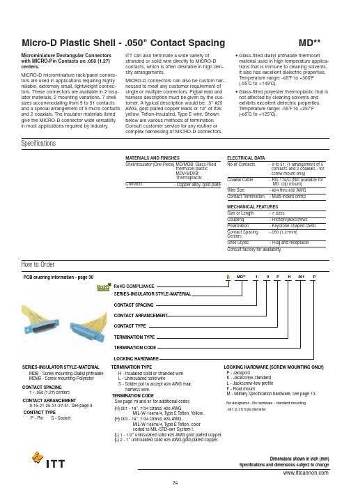
PCB ordering information - page 30SERIES-INSULATOR STYLE-MATERIAL SERIES-INSULATOR STYLE-MATERIALMDB - Screw mounting-Diallyl phthalate MDVB - Screw mounting-Polyester H -Insulated solid or stranded wire L -Uninsulated solid wireS -Solder pot to accept #26 AWG max.harness wire.No designator - No hardware - standard mounting .091 (2.31) hole diameterP -JackpostK -Jackscrew-standard L -Jackscrew-low profile F -Float mountM -Military specification hardware, see page 13.1-.050 (1.27) centers9-15-21-25-31-37-51. See page 9P -Pin S - SocketCONTACT SPACIN GCONTACT ARRAN G EMENTCONTACT TYPECONTACT SPACIN G CONTACT ARRAN G EMENT CONTACT TYPE TERMINATION TYPE TERMINATION TYPELOC K IN G H AR DW ARE (SCRE W MOUNTIN GONLY )TERMINATION CO D E LOC K IN G H AR DW AREM D** 1-9P H 001P(H) 001 - 18",7/34strand, #26 AWG, MIL-W-16878/4,T ype E T eflon, Y ellow.(H) 003 - 18",7/34strand, #26 AWG, MIL-W-16878/4,T ype E T eflon, color coded to MIL-S T D-681System I.(L) 1 - 1/2"uninsulated solid #25 AWG gold plated copper.(L) 2 - 1"uninsulated solid #25 AWG gold plated copper.TERMINATION CO D ERo H S COMPLIANCERSee page 79 and 81for additional codesDimensions shown in inch (mm)Specifications and dimensions subject to changeHow to OrderMicrominiature Rectangular Connectors with MICRO-Pin Contacts on .050 (1.27)centers.MICRO-D microminiature rack/panel connec-tors are used in applications requiring highly reliable, extremely small, lightweight connec-tors. These connectors are available in 2 insu-lator materials, 2 mounting variations, 7 shell sizes accommodating from 9 to 51 contacts and a special arrangement of 5 micro contacts and 2 coaxials. The insulator materials listed give the MICRO-D connector wide versatility in most applications required by industry.ITT can also terminate a wide variety of stranded or solid wire directly to MICRO-D contacts, which is often desirable in high den-sity arrangements.MICRO-D connectors can also be custom har-nessed to meet any customer requirement of single or multiple connectors. Pigtail lead and harness description must be given by the cus-tomer. A typical description would be: .5" #25AWG, gold plated copper leads or 18" of #26yellow, Teflon-insulated, Type E wire. Shown below are various methods of termination.Consult customer service for any routine or complex harnessing of MICRO-D connectors.•Glass-filled diallyl phthalate thermoset material used in high temperature applica-tions that is immune to cleaning solvents.It also has excellent dielectric properties.Temperature range: -65˚F to +300˚F (-55˚C to +149˚C).•Glass-filled polyester thermoplastic that is not affected by cleaning solvents and exhibits excellent dielectric properties.Temperature range: -55˚F to +257˚F (-65˚C to +125˚C).SpecificationsMATERIALS AND FINISHESShell/Insulator (One Piece)MD/MDB: Glass-filledthermoset plastic MDV/MDVB: Thermoplastic ELECTRICAL DATA MECHANICAL FEATURES No of ContactsSize or Length Coupling PolarizationContact Spacing Centers Shell StylesConsult factory for availabilty.Coaxial CableWire SizeContact Termination -9to 51: (1 arrangement of 5 contacts and 2 coaxials - for screw mount only)-7sizes-Friction/jackscrews-Keystone-shaped shells -.050 (1.27mm)-Plug and receptacle-RG-178/U (Not available for MD clip mount)-#24 thru #32 AWG -Multi-indent crimp-Copper alloy, gold plateContactsDimensions shown in inch (mm)Specifications and dimensions subject to changeStandard Wire Termination CodesCavity #1 black*The following termination codes are listed for your information. For additional codes please refer to Appendix on page 79 and 81. All wire lengths are minimum.#26 A WG per MIL-W-16878 Type E Teflon ,stranded.H arness Typ e (H)L ength 3(76.2)6(152.4)8(203.2)10(254.0)12(304.8)18 (457.2)20(508.0)24(609.6)30(762.0)36(914.4)48(1219.2)72(1828.8)120(3048.0)H020H019H026H029H028H001H038H009H010H011H013H017H042H027H016H034H025H002H003H023H004H005H006H048H046H041L61L 56L 57L 39L 58L 1L 14L2L 7L6L 16L 10.125(3.18).150 (3.81).190(4.83).250 (6.35).375(9.52).500 (12.70).750 (19.05)1.000 (25.40)1.500 (38.10)2.000 (50.80)2.500 (63.50)3.000 (76.20)All Y ell o w Co l o r Cod e d*T erminati o n Cod eL ength #25A WG G old P lated CopperS o li d U ninsulate d Typ e (L)With Screw Mounting Holes (Conforms to MIL-DTL-83513)MDB.110(2.79)MAX..154(3.91)(5.08)MAX.Solder PotSolder PotGlass-filled Diallyl Phthalate Plastic InsulatorMDVBGlass-filled Polyester Plastic InsulatorRPart Number by Shell Size Add lead type and length, see Part Number Explanation.Weight given is with 1/2", uninsulated solid #25 AWG gold plated copper pigtails.*****AMax.B Max.C Max.D Max.E Max.F ±.005Avg.Weight***±5% (oz.)±5% (gm.)MDB1-9S**MDB1-15P**MDB1-15S**MDB1-21P**MDB1-21S**MDB1-25P**MDB1-25S**MDB1-31P**MDB1-31S**MDB1-37P**MDB1-37S**MDB1-51P**MDB1-51S**MDVB1-9S**MDVB1-15p**MDVB1-15S**MDVB1-21P**MDVB1-21S**MDVB1-25P**MDVB1-25S**MDVB1-31P**MDVB1-31S**MDVB1-37P**MDVB1-37S**MDVB1-51P**MDVB1-51S**.788 (20.02).788 (20.02).938 (23.82)1.088 (27.64)1.088 (27.64)1.188 (30.18)1.188 (30.18)1.338 (33.98)1.338 (33.98)1.488 (37.80)1.488 (37.80)1.438 (36.52)1.438 (36.52).292 (7.42).380 (9.65).442 (11.23).592 (15.04).680 (17.27).692 (17.58).780 (19.81).842 (21.39).930 (23.62).992 (25.20)1.080 (27.43).942 (23.93)1.030 (26.16).408 (10.36).408 (10.36).588 (14.17).708 (17.98).708 (17.98).808 (20.56).808 (20.56).958 (24.33).958 (24.33)1.108 (28.14)1.108 (28.14)1.058 (26.87)1.058 (26.87).173 (4.39).173 (4.39).173 (4.39).173 (4.39).173 (4.39).173 (4.39).173 (4.39).173 (4.39).173 (4.39).173 (4.39).173 (4.39).220 (5.59).220 (5.59).218 (5.54).218 (5.54).218 (5.54).218 (5.54).218 (5.54).218 (5.54).218 (5.54).218 (5.54).218 (5.54).218 (5.54).218 (5.54).260 (6.60).260 (6.60).565 (14.35).565 (14.35).715 (18.16).865 (21.97).865 (21.97).965 (24.51).965 (24.51)1.115 (28.32)1.115 (38.32)1.265 (32.13)1.265 (32.13)1.215 (30.86)1.215 (30.86).026 (0.73).025 (0.70).038 (1.10).053 (1.50).050 (1.40).063 (1.80).056 (1.60).080 (2.30).073 (2.10).086 (2.45).076 (2.15).109 (3.10).093 (2.64)Dimensions shown in inch (mm)Specifications and dimensions subject to changeMD*B-PCB connectors use standard MD*B all plastic shells and are designed for use with flex circuitry, printed circuit and multi-layer boards. They are easily mounted and soldered and provide high density/high reliability in board-to-board and board-to-cable applica-tions. While being similar to the MDM-PCB connectors, the MD*B-PCB connectors are all plastic, extremely small, and lightweight yet rugged enough for use in the most demanding applications.MD*B-PCB connectors are available inseven shell sizes with 9 to 51 contacts in the popular 90°narrow profile PCB termination,with a variety of tail lengths for varying boardthickness.How to OrderSERIESCONTACT ARRANGEMENT CONTACT TYPE CTERMINATION TYPE THARDWAREHTERMINATION TAIL LENGTH TMODIFICATION CODES C(Consult Factory)MMD*B--37S CBR ** * *L39RoHS COMPLIANCE RJackpost mounting for use with locking hard-ware is also available.If the connectors shown in the catalog do not meet the requirements of your applica-tions, a special shape, size or layout using the basic all plastic shell can be made avail-able. For further technical and applications information, contact customer service.CONNECTOR SERIES MDVB, MDBCONNECTOR ARRANGEMENT9, 15, 21, 25, 31, 51CONTACT TYPES =Socket P =PinTERMINATION TYPECBR = 90°Narrow Profile PCB Terminations HARDWAREP =JackpostM7 = Jackposts, M635135-07No Letter = Less HardwareTERMINATION TAIL LENGTH CODESNONE –.109 (2.77) ±0.15 (0.38) Standard L61– .125 (3.18)L66– .150 (3.81)L57– .190 (4.83)L39–.250 (6.35)L58– .375 (9.52)Dimensions shown in inch (mm)Specifications and dimensions subject to changeCBR Series (90˚ Mounting Narrow Profile)TYP ..186 (4.72) PLUG 9-15-21-25 VIEW*FOR 31: 1.085 (27.56) MAX. FOR 37: 1.185 (30.10) MAX. FOR 51: 1.225 (31.12) MAX.I A. TYPPCB Termination Arrangements (Viewed from bottom of connector, on PCB solder side.)Indentification number shown for plug connector, use reverse order for socket connector..083.020.0209Contacts15 Contacts21 Contacts 25Contacts51 Contacts37 Contacts31 ContactsAll Termination Configurations .100 (2.54) x .100 (2.54) Grid Pattern, Offset .050 (1.27)*For jackpost locking add letter "P" or "M7".NOTE: Standard lead termination is #24 AWG, solid copper, solder or tin dipped.Part Number By Shell Size MD*B-9PCBR*MD*B-9SCBR*MD*B-15PCBR*MD*B-21PCBR*MD*B-21SCBR*MD*B-25PCBR*MD*B-25SCBR*MD*B-31PCBR*MD*B-31SCBR*MD*B-37PCBR*MD*B-37SCBR MD*B-51PCBR*MD*B-51SCBR.788 (20.01).938 (23.82)1.088 (27.63)1.088 (27.63)1.188 (30.17)1.188 (30.17)1.338 (33.98)1.338 (33.98)1.488 (37.79)1.488 (37.79)1.438 (36.52)1.438 (36.52).565 (14.35).715 (18.16).865 (21.97).865 (21.97).965 (24.51).965 (24.51)1.115 (28.32)1.115 (28.32)1.265 (32.13)1.265 (32.13)1.215 (30.86)1.215 (30.86).292 (7.42).525 (13.34).592 (15.04).675 (17.14).692 (17.58).775 (19.68).842 (21.39).925 (23.50).994 (25.25)1.075 (27.30).942 (23.93)1.026 (26.06).218 (5.54).218 (5.54).218 (5.54).218 (5.54).218 (5.54).218 (5.54).218 (5.54).218 (5.54).218 (5.54).218 (5.54).258 (6.55).258 (6.55).134 (3.40).218 (5.54).134 (3.40).218 (5.54).134 (3.40).218 (5.54).134 (3.40).218 (5.54).134 (3.40).218 (5.54).177 (4.50).258 (6.55).420 (10.67).420 (10.67).420 (10.67).420 (10.67).420 (10.67).420 (10.67).420 (10.67).420 (10.67).520 (13.21).520 (13.21).550 (13.97).550 (13.97).250 (6.35).250 (6.35).250 (6.35).250 (6.35).250 (6.35).250 (6.35).250 (6.35).250 (6.35).250 (6.35).250 (6.35).300 (7.62).300 (7.62).230 (5.84).130 (3.30).130 (3.30).130 (3.30).130 (3.30).130 (3.30).130 (3.30).130 (3.30).130 (3.30).130 (3.30).150 (3.81).150 (3.81)A Max.B±.005 (0.13)G±.010 (0.25)H±.010 (0.25)C Max.D Max.E Max.F Max.Dimensions shown in inch (mm)MDB Coaxial Series with Screw Mounting HolesMDB connectors with two coaxial and five MICRO-PIN TM /MICROSOCKET TM contacts. Crimp-type coaxial contacts accommodate RG-178/U cables. A plastic insertion/extraction tool is supplied with each connec-tor assembly having removable coaxial assembly.How to Order - MDB CoaxialSERIESMDB1-7C2****SHKSERIESMicro-D CoaxialNo Letter - Coaxial assemblyinstalled and nonremovable RO - coaxial assembly ordered serparatelyRA - Coaxial shipped assembled but uninstalled See Standard Wire TerminationConsult customer serviceNo letter - No hardware*Not available with removalbe coax cable type connectors RO and RA.standard mounting. 091 (2.31) hole diameter F -FloatK -Jackscrew (standard)L -Jackscrew (low profile)P -JackpostCode on page 29. Coaxial cable will beRG-178U unless otherwise specified; length will be same as wire modification.P -Pin S -Socket L -Uninsulated, solid wireH -Insulated, solid or stranded S -Solder pot*1-.050 (1.27) centers...................7 (2)SIGNAL CONTACT SPACING TOTAL CONTACT CAVITIES NUMBER OF COAXIALS SIGNAL CONTACT SPACING TOTAL CONTACT CAVITIES NUMBER OF COAXIALS COAXIAL TYPECOAXIAL TYPESIGNAL CONTACT TYPE SIGNAL CONTACT TYPESIGNAL CONTACT LEAD TYPE SIGNAL CONTACT LEAD TYPESIGNAL CONTACT LEAD LENGTH SIGNAL CONTACT LEAD LENGTH MODIFICATIONHARDWAREMODIFICATION HARDWARERoHS COMPLIANCE RHow to Order - Coaxial Cable AssembliesSERIESMDCCS** * *COAXIAL CABLE CONTACT TYPE CONTACT TYPE COAXIAL CABLE TYPECOAXIAL CABLE TYPE COAXIAL CABLE LENGTHCOAXIAL CABLE LENGTHSERIES MDP -Pin(used with socket side connection)S -Socket(used with pin type connection)See Standard Wire TerminationCodes on page 29. Coaxial cable will be RG-178U unless otherwise specified; length will be the same as wire modfication.1-RG178/UCOAXIAL CABLE CCRoHS COMPLIANCE RDimensions shown in inch (mm)Specifications and dimensions subject to changeDimension - MDB Coaxial SeriesPlugReceptacle(See page 9 for layouts)Part Numberby Shell SizeMDB1-7C2P*MDB1-7C2S*.510 (12.95).602 (15.29)* Add lead type and length, see Part Number Explanation.** Weight given is with 7 inch (177.80) insulated leads, #26 AWG silver plated copper pigtails and RG178/U coaxials..204 (5.18).185 (4.70).298 (7.57).279 (7.09).782 (19.86).782 (19.86).395 (10.03).375 (9.52).510 (12.95).540 (13.72).290 (8.30).273 (7.80)A Ma x.B Ma x.C Ma x.E Ma x.E 1Ma x.D +_.005 (0.13)Av g .W eight**(oz)+_5% (gm .)+_5%TWO MTG. HOLES RO AND RA COAXESRO AND RA COAXESMounting Hardware Views (Sizes 9-51)This hardware supplied unassembled.Screw Lock Assembly90˚ Angle Mounting BracketDescriptionScrew Lock Assembly Jackpost Kit322-9500-000 320-9505-000015-9516-000 .100 (2.54) .122 (3.10) .257(6.53).215(5.46)015-9516-000 Mounting Bracket, 90˚ Angle- MD*1for 9 thru 37 Shell Sizes MD*1for 51 Shell SizeNOTES: Screw lock assembly (322-9500-000) can be used for front front mounting. Jackpost kit(320-9505-000) consists of 2 assemblies, shipped unassembled.Part Number ±.005 (0.13)Max.*NOTE: Torque value is 4.0 in/lbs max. REF. ONLY_.003_0.08)FACEFACECONNECTOR HEX HEAD -Jackscrew - (L) Low ProfileJackscrew - (K) StandardThis hardware is factory installed.Shown here is a cutaway view of the float mount for the MD connector.The basic shell dimensions are the same for the float mount and the screw mounting hole configurations. View shown is for standard float mount front panel mounting. Reverse mounting is available on request.*NOTE: Torque values are as follows: Low Profile Jackscrew (L)-2.5 in/lbs Standard Jackscrew (K)-2.5 in/lbsDimensions shown in inch (mm)Specifications and dimensions subject to changeMounting Hardware to Military Specification (Sizes 9 - 51) PER MIL-DTL-83513/5This hardware supplied unassembled.Jackscrew - (L) Low profile *.062 (1.57)HEX. (REF.).092 (2.34) DIA.Allen headPlug and Receptacle Low and High Profile Slotted HeadJackpost AssemblyDescriptionSlotted Head Jackscrew Assy Low ProfileSlotted Head Jackscrew Assy High Profile Allen Head Jackscrew Assy Low Profile Allen Head Jackscrew Assy High Profile Jackpost Assy-05-06-02-03-07M5M6M2M3M7320-9508-025320-9508-027320-9508-026320-9508-028320-9505-033M83513/5Mode Code Part Number ThreadJackpost Bushing (For Rear Panel Mounting)MATING FACE.126 (3.20).125 (3.18)DIA.TYP .+.005 (0.13)3/32 (2.4)1/16 (1.6)3/64 (1.2)1/32 (0.8).092/.087 (2.34/2.21).061/.056 (2.34/1.42).047/.042 (1.19/1.07).030/.025 (0.76/0.64)320-9505-007320-9505-006320-9505-005320-9505-0049152125313751.379 ( 9.63).529 (13.44).679 (17.25).779 (19.79).929 (23.60)1.079 (27.41)1.029 (26.14).219 (5.56).219 (5.56).219 (5.56).219 (5.56).219 (5.56).219 (5.56).261 (6.63).565 (14.35).715 (18.16).865 (21.97).965 (24.51)1.115 (28.32)1.265 (32.13)1.215 (30.86)*2Jackposts, 2nuts, 2washers .Panel Thickness A Dim.Jackpost Kit Number*A+.004 (0.10)-.000 (0.00)Shell SizePlug and Receptacle DimensionsB +.004 (0.10)-.000 (0.00)C +_.005(0.13)NOTE: Torque value for jackpost 2.5 in /lbsPanel Mounting Dimensions.200 ±.005Plug and ReceptacleRear MountedPlug and Receptacle Front Mounted Plug Front Mounted Receptacle Rear Mounted.300 ±.005Dimensions shown in inch (mm)Specifications and dimensions subject to changePanel CutoutsFigure 1Front Mounting+.005 (0.13) R TYP -.000 (0.00)Figure 2Rear MountingFigure 3Edgeboard MountingNOTES:1. 2. 3. 123123123123123123123.409 (10.39).379 ( 9.63)-.559 (14.20).529 (13.44)-.709 (18.00).679 (17.25)-.809 (20.55).779 (19.79)-.959 (24.36).929 (23.60)-1.109 (28.17)1.079 (27.41)-1.059 (26.90)1.029 (26.14)-.172 (4.37).219 (5.56)-.172 (4.37).219 (5.56)-.172 (4.37).219 (5.56)-.172 (4.37).219 (5.56)-.172 (4.37).219 (5.56)-.172 (4.37).219 (5.56)-.215 (5.46).261 (6.63)-.570 (14.48).570 (14.48).570 (14.48).720 (18.29).720 (18.29).720 (18.29).870 (22.10).870 (22.10).870 (22.10).970 (24.64).970 (24.64).970 (24.64)1.120 (28.45)1.120 (28.45)1.120 (28.45)1.270 (32.26)1.270 (32.26)1.270 (32.26)1.220 (30.99)1.220 (30.99)1.220 (30.99).089 (2.26).089 (2.26).089 (2.26).089 (2.26).089 (2.26).089 (2.26).089 (2.26).089 (2.26).089 (2.26).089 (2.26).089 (2.26).089 (2.26).089 (2.26).089 (2.26).089 (2.26).089 (2.26).089 (2.26).089 (2.26).089 (2.26).089 (2.26).089 (2.26)9152125313751A+.004 (0.10)-.000 (0.00)B+.004 (0.10)-.000 (0.00)C+.005 (0.13)-.000 (0.00)D+.005 (0.13)-.000 (0.00)Cutout Figure Size Front mounting (figure 1) and rear mounting (figure 2) accommodates #2-56 screws.Front mounting is preferred. However, when rear mounting is necessary. use detail on previous page.Edgeboard mounting bracket (figure3) uses #2-56 screws. Dimension .450 ± .002 (11.43 ± 0.05) locates theMD receptacle flush with the end of the board.PlugMDGlass-filled Diallyl Phthalate Plastic InsulatorMDVGlass-filled Polyester Plastic InsulatorSolder PotSolder PotReceptacle.130(3.30)(5.33)(4.32).170(4.32)PCB ordering information - page 30SERIES-INSULATOR STYLE-MATERIAL SERIES-INSULATOR STYLE-MATERIALMD - Clip mounting -Diallyl phthalate MDV - Clip mounting-Polyester H-Insulated solid or stranded wire L -Uninsulated solid wireS -Solder pot to accept #26 AWG max.harness wire.No designator - No hardware - standard mounting .091 (2.31) hole diameterNot available in clip mounting.See page 79 and 81for additional codes.***(H) 001 - 18", 7/34strand ,#26 AWG ,MIL-W-16878/4, T ype E T eflon ,Y ellow.(H) 003 - 18", 7/34strand ,#26 AWG ,MIL-W-16878/4, T ype E T eflon ,colorcoded to MIL-S T D-681 System I.(L) 1 - 1/2"uninsulated solid #25AWG gold plated copper.(L) 2 - 1"uninsulated solid #25AWG gold plated copper.1-.050(1.27) centers9-15-21-25-31*-37-51.See page 7P -Pin S - Soc k etCONTACT SPACIN GCONTACT ARRAN G EMENTCONTACT TYPECONTACT SPACIN G CONTACT ARRAN G EMENT CONTACT TYPE TERMINATION TYPE TERMINATION TYPETERMINATION CO D E **TERMINATION CO D E LOC K IN G H AR DW AREM D1-9PH001PRo H S COMPLIANCERPart Number by Shell Size MD1-9P**MD1-9S**MD1-15P**MD1-15S**MD1-21P**MD1-21S**MD1-25P**MD1-25S**MD1-37P**MD1-37S**MD1-51P**MD1-51S**MDV1-9-P**MDV1-9S**MDV1-15P**MDV1-15S**MDV1-21P**MDV1-21S**MDV1-25P**MDV1-25S**MDV1-37P**MDV1-37S**MDV1-51P**MDV1-51S**A Max.B Max.C Max.D Max.E Max.Avg. Weight***±5% (oz.)/±5% (gm.).512 (13.00).512 (13.00).662 (16.81).662 (16.81).812 (20.62).812 (20.62).912 (23.16).912 (23.16)1.212 (30.78)1.212 (30.78)1.162 (29.51)1.162 (29.51).292 (7.42).376 (9.55).442 (11.23).526 (13.36).592 (15.04).676 (17.17).692 (17.58).776 (19.71).992 (25.20)1.076 (27.33).942 (23.93)1.026 (26.06).405 (10.29).405 (10.29).555 (14.10).555 (14.10).705 (17.91).705 (17.91).805 (20.45).805 (20.45)1.105 (28.07)1.105 (28.07)1.055 (26.80)1.055 (26.80).170 (4.32).170 (4.32).170 (4.32).170 (4.32).170 (4.32).170 (4.32).170 (4.32).170 (4.32).170 (4.32).170 (4.32).213 (5.41).213 (5.41).215 (5.46).215 (5.46).215 (5.46).215 (5.46).215 (5.46).215 (5.46).215 (5.46).215 (5.46).215 (5.46).215 (5.46).258 (6.55).258 (6.55).026 (0.73).026 (0.73).038 (1.10).035 (1.00).053 (1.50).050 (1.40).063 (1.80).056 (1.60).086 (2.45).076 (2.15).109 (3.10).093 (2.65)How to OrderWith Clip Mounting SlotsMicro-D Plastic Shell - .050" Contact Spacing MD**Panel Mounting HardwareClip MountingDescriptionDimensions (Clip Mounting Only)Coupling Retention Clip(see Figure 2)Mounting Screw Brackets(see Figures 1 and 3)PanelMounting KeyEdgeboard Mounted(see Figure 4)Plug and ReceptacleRear MountedPlug and ReceptacleFront Mounted Receptacle Rear MountedPart Number201-9100-000294-9100-000015-9100-000015-5009-000MD51428-1Panel Mounting KeyMounting Key and Coupling Clip AssemblyMounting Screw BracketEdgeboard Mounting BracketEdgeboard Mounting Bracket andCoupling Clip AssemblyMust be ordered separately; specify left and right hand for completeassembly.Must be ordered separately; assembly contains set of left and righthand types.******Illustrated is the recommended method of front mountingwith metal panel mounting keys. Panel mounting keys areavailable with or without coupling retention clips.For front mounting,place the rear of the connector thruthe panel cutout.With the mounting flange against thepanel,fully insert the panel mounting keys thru the slotsin the flange and thru the panel cutout.Retaining thekeys in this position, bend them outward against the rearof the panel.When mating a front mounted connectorwith an unmounted connector, a coupling retention clipassembly may be used to securely lock the two together.Mounting screw brackets are available and may be usedinstead of the panel mounting keys.Panel CutoutsFigure 1Figure 3Rear MountingFigure 4Edgeboard MountingFigure 2Front Mounting.).).MAX. (TYP.)A panel thickness of 1/8" 3.17mm) maximum is recommended for ease of tab bendingwhen a panel mounting key & clip assembly or edgeboard mounting brackets are used.Front mounting is preferred. However, when rear mounting is necessary, use figure 3 fordimensions.Figure 4 is for edge board mounting bracket or edgeboard clip assembly. The .184 +_ .0022.67 +_ 0.05) dimension locates the MD socket insulator flush with the end of the board.Screw brackets (015-9100-000) will accommodate #2-56 screws.Front mounting(Figure 1)and rear mounting(Figure 3)accommodate#2-56screws.1.2.3.4.5.ShellSize91521253751123412341234123412341234.408 (10.36).408 (10.36).378 ( 9.60).400 (10.16).588 (14.94).588 (14.94).528 (13.28).550 (13.97).738 (18.75).738 (18.75).678 (17.27).700 (17.78).838 (21.29).838 (21.29).778 (19.76).800 (20.32)1.138 (28.91)1.138 (28.91)1.078 (27.38)1.100 (27.94)1.088 (27.64)1.088 (27.64)1.028 (26.11)1.050 (26.67).172 (4.37).172 (4.37).217 (5.51).091 (2.31).172 (4.37).172 (4.37).217 (5.51).091 (2.31).172 (4.37).172 (4.37).217 (5.51).091 (2.31).172 (4.37).172 (4.37).217 (5.51).091 (2.31).172 (4.37).172 (4.37).217 (5.51).091 (2.31).215 (5.46).215 (5.46).260 (6.60).091 (2.31).650 (16.51)-.650 (16.51)-.795 (20.19)-.795 (20.19)-.945 (24.00)-.945 (24.00)-1.045 (26.54)-1.045 (26.54)-1.345 (34.16)-1.345 (34.16)-1.295 (32.89)-1.295 (32.89)-.089 (2.26)-.089 (2.26)-.089 (2.26)-.089 (2.26)-.089 (2.26)-.089 (2.26)-.089 (2.26)-.089 (2.26)-.089 (2.26)-.089 (2.26)-.089 (2.26)-.089 (2.26)-CutoutFigureA+.004 (0.10)-.000 (0.00)B+.004 (0.10)-.000 (0.00)C+.004 (0.10)-.000 (0.00)D+.005 (0.13)-.000 (0.00)38Dimensions shown in inch (mm)Specifications and dimensions subject to change 元器件交易网。
601S0275中文资料

© Faraday Technology. As part of continual product improvement the specifications, details and dimensions shown in this publication are subject to change without noticeDesigned to meet the full requirements of Rec. ITU-R BT. 601-5 to suppress aliasing and to reconstruct signals in 4:2:2 YUV format A-D and D-A video interface applications operating at standard sampling rates of 13.5 MHz for the luminance (Y) channel and 6.75 MHz for the Colour Difference (U and V) channels.• Fully compliant with ITU-R BT601• Industry Standard Footprint • Tighter delay time tolerances available• Tight passband ripple specificationType Number 601F0575601S0575601F0275 601S0275Impedance (ohms)75757575Filter Shape Lowpass Lowpass LowpassLowpass Passband Shape Flat Sinx/x Flat Sinx/x Sampling Frequency13.50 MHz13.50 MHz 6.75 MHz6.75 MHz Insertion loss at 100 kHz < 1.5 dB < 4.5 dB < 1.5 dB< 4.5 dB End of Passband 5.75 MHz5.75 MHz2.75 MHz2.75 MHzAmplitude ripple (dB)<± 0.025 to 5.50 MHz <± 0.0251 to 5.50 MHz <± 0.050 to 2.75 MHz <± 0.0502 to 2.75 MHz wrt 100 kHz<± 0.050 to 5.75 MHz <± 0.0501 to 5.50 MHz Delay time at 200 kHz 760 ± 7nS 758 ± 7nS1488 ± 14 ns1486 ± 14 nsGroup delay ripple<±3nS to 5.75 MHz <±3 nS to 5.75 MHz<± 6 nS to 2.75 MHz <± 6 nS to 2.75 MHz wrt delay at 200 kHz<±12 nS to 3.0 MHz <± 12 nS to 3.0 MHz Attenuation at 1/2 S.F.> 12 dB > 12 dB 1 > 6 dB> 6 dB 2wrt loss at 100 kHzStart of stopband 8.00 MHz 8.00 MHz 4.00 MHz 4.00 MHz Stopband attenuation> 40 dB> 40 dB> 40 dB> 40 dBwrt loss at end of passbandAqueous Washable 3No No No No Package sizeDR00003ADR00003ADR00003ADR00003A1Measured against sinx/x roll-off for a sampling frequency of 13.5 MHz.2Measured against sinx/x roll-off for a sampling frequency of 6.75 MHz.3Contact Faraday for Washable options.ITU-R BT. 601 FILTERS Appendix 2 – Part AYUV ANTIALISING – STANDARD FOOTPRINTPACKAGE DETAILFaraday Technology Ltd.Tel:+ 44 (0)1782 661501Croft Road Industrial Estate,Fax:+ 44 (0)1782 630101Newcastle, Staffordshire Email:sales@ ST5 0QZ. England.Web site:。
PBSS5160T,215;中文规格书,Datasheet资料

Product data sheet Supersedes data of 2003 Jun 242004 May 12NPN low V CEsat (BISS) transistorPBSS4160TFEATURES•Low collector-emitter saturation voltage V CEsat•High collector current capability I C and I CM•High efficiency, reduces heat generation•Reduces printed-circuit board area required•Cost effective replacement for medium power transistor BCP55 and BCX55.APPLICATIONS•Major application segments:–Automotive 42 V power–Telecom infrastructure–Industrial.•Power management:–DC-to-DC conversion–Supply line switching.•Peripheral driver–Driver in low supply voltage applications (e.g. lamps and LEDs)–Inductive load driver (e.g. relays,buzzers and motors).DESCRIPTIONNPN low V CEsat transistor in a SOT23 plastic package. PNP complement: PBSS5160T.MARKINGNote1.* = p: made in Hong Kong* = t: made in Malaysia* = W: made in China.QUICK REFERENCE DATA PINNINGTYPE NUMBER MARKING CODE(1) PBSS4160T*U5SYMBOL PARAMETER MAX.UNIT V CEO collector-emitter voltage60VI C collector current (DC)1AI CM peak collector current2AR CEsat equivalent on-resistance250mΩPIN DESCRIPTION1base2emitter3collectorORDERING INFORMATIONTYPE NUMBERPACKAGENAME DESCRIPTION VERSIONPBSS4160T−plastic surface mounted package; 3 leads SOT23NPN low V CEsat (BISS) transistorPBSS4160TLIMITING VALUESIn accordance with the Absolute Maximum Rating System (IEC 60134).Notes1.Device mounted on an FR4 printed-circuit board, single-sided copper, tin-plated, standard footprint.2.Device mounted on an FR4 printed-circuit board, single-sided copper, tin-plated, 1 cm 2 collector mounting pad.3.Operated under pulsed conditions: duty cycle δ ≤ 20%, pulse width t p ≤ 10 ms.SYMBOL PARAMETERCONDITIONSMIN.MAX.UNITV CBO collector-base voltage open emitter −80V V CEO collector-emitter voltage open base −60V V EBO emitter-base voltage open collector −5V I C collector current (DC)note 1−0.9A note 2−1A I CM peak collector current t = 1 ms or limited by T j(max)−2AI B base current (DC)−300mA I BM peak base current t p ≤ 300 μs; δ ≤ 0.02−1A P tottotal power dissipationT amb ≤ 25 °C; note 1−270mW T amb ≤ 25 °C; note 2−400mW T amb ≤ 25 °C; notes 1 and 3− 1.25W T stg storage temperature −65+150°C T j junction temperature−150°C T amb operating ambient temperature−65+150°CNPN low V CEsat (BISS) transistorPBSS4160TTHERMAL CHARACTERISTICS Notes1.Device mounted on an FR4 printed-circuit board, single-sided copper, tin-plated and standard footprint.2.Device mounted on an FR4 printed-circuit board, single-sided copper, tin-plated and 1 cm 2 collector mounting pad.3.Operated under pulsed conditions: duty cycle δ ≤ 20%, pulse width t p ≤ 10 ms.SYMBOL PARAMETERCONDITIONSVALUE UNIT R th(j-a)thermal resistance from junction to ambientin free air; note 1465K/W in free air; note 2312K/W in free air; notes 1 and 3100K/WNPN low V CEsat (BISS) transistorPBSS4160TCHARACTERISTICST amb = 25 °C unless otherwise specified.Note1.Pulse test: t p ≤ 300 μs; δ ≤ 0.02.SYMBOL PARAMETERCONDITIONSMIN.TYP.MAX.UNIT I CBO collector-base cut-off current V CB = 60 V; I E = 0 A−−100nA V CB = 60 V; I E = 0 A; T j = 150 °C −−50μA I CES collector-emitter cut-off current V CE = 60 V; V BE = 0 A −−100nA I EBO emitter-base cut-off current V EB = 5 V; I C = 0 A −−100nAh FEDC current gainV CE = 5 V; I C = 1 mA250400−V CE= 5 V; I C = 500 mA; note 1200350−V CE = 5 V; I C = 1 A; note 1100150−V CEsatcollector-emitter saturation voltageI C = 100 mA; I B = 1 mA −90110mV I C = 500 mA; I B = 50 mA −110140mV I C = 1 A; I B = 100 mA; note 1−200250mV V BEsat base-emitter saturation voltage I C = 1 A; I B = 50 mA −0.95 1.1V R CEsat equivalent on-resistance I C = 1 A; I B = 100 mA; note 1−200250m ΩV BEon base-emitter turn-on voltage V CE = 5 V; I C = 1 A −0.820.9V f T transition frequency I C = 50 mA; V CE = 10 V; f = 100 MHz150220−MHz C c collector capacitanceV CB = 10 V; I E = I e = 0 A; f = 1 MHz −5.510pFPBSS4160T NPN low V CEsat (BISS) transistorPBSS4160T NPN low V CEsat (BISS) transistorPBSS4160T NPN low V CEsat (BISS) transistorPACKAGE OUTLINENPN low V CEsat (BISS) transistorPBSS4160TDATA SHEET STATUSNotes1.Please consult the most recently issued document before initiating or completing a design.2.The product status of device(s) described in this document may have changed since this document was publishedand may differ in case of multiple devices. The latest product status information is available on the Internet at URL . DOCUMENT STATUS (1)PRODUCT STATUS (2)DEFINITIONObjective data sheet Development This document contains data from the objective specification for product development.Preliminary data sheet Qualification This document contains data from the preliminary specification. Product data sheet ProductionThis document contains the product specification.DISCLAIMERSGeneral ⎯ Information in this document is believed to be accurate and reliable. However, NXP Semiconductors does not give any representations or warranties,expressed or implied, as to the accuracy or completeness of such information and shall have no liability for the consequences of use of such information.Right to make changes ⎯ NXP Semiconductors reserves the right to make changes to informationpublished in this document, including without limitation specifications and product descriptions, at any time and without notice. This document supersedes and replaces all information supplied prior to the publication hereof.Suitability for use ⎯ NXP Semiconductors products are not designed, authorized or warranted to be suitable for use in medical, military, aircraft, space or life support equipment, nor in applications where failure or malfunction of an NXP Semiconductors product can reasonably be expected to result in personal injury, death or severe property or environmental damage. NXP Semiconductors accepts no liability for inclusion and/or use of NXP Semiconductors products in such equipment orapplications and therefore such inclusion and/or use is at the customer’s own risk.Applications ⎯ Applications that are described herein for any of these products are for illustrative purposes only. NXP Semiconductors makes no representation or warranty that such applications will be suitable for the specified use without further testing or modification.Limiting values ⎯ Stress above one or more limiting values (as defined in the Absolute Maximum Ratings System of IEC 60134) may cause permanent damage to the device. Limiting values are stress ratings only and operation of the device at these or any other conditions above those given in the Characteristics sections of this document is not implied. Exposure to limiting values for extended periods may affect device reliability.Terms and conditions of sale ⎯ NXP Semiconductors products are sold subject to the general terms and conditions of commercial sale, as published at /profile/terms, including those pertaining to warranty, intellectual property rightsinfringement and limitation of liability, unless explicitly otherwise agreed to in writing by NXP Semiconductors. In case of any inconsistency or conflict between information in this document and such terms and conditions, the latter will prevail.No offer to sell or license ⎯ Nothing in this document may be interpreted or construed as an offer to sell products that is open for acceptance or the grant, conveyance or implication of any license under any copyrights, patents or other industrial or intellectual property rights.Export control ⎯ This document as well as the item(s) described herein may be subject to export controlregulations. Export might require a prior authorization from national authorities.Quick reference data ⎯ The Quick reference data is an extract of the product data given in the Limiting values and Characteristics sections of this document, and as such is not complete, exhaustive or legally binding.NXP SemiconductorsCustomer notificationThis data sheet was changed to reflect the new company name NXP Semiconductors, including new legal definitions and disclaimers. No changes were made to the technical content, except for package outlinedrawings which were updated to the latest version.Contact informationFor additional information please visit: For sales offices addresses send e-mail to: salesaddresses@© NXP B.V. 2009All rights are reserved. Reproduction in whole or in part is prohibited without the prior written consent of the copyright owner.The information presented in this document does not form part of any quotation or contract, is believed to be accurate and reliable and may be changed without notice. No liability will be accepted by the publisher for any consequence of its use. Publication thereof does not convey nor imply any license under patent- or other industrial or intellectual property rights.Printed in The Netherlands R75/02/pp10 Date of release: 2004 May 12 Document order number: 9397 750 13198分销商库存信息: NXPPBSS5160T,215。
Leica_TS15用户手册

激光指向
• 多款 TS15 具有自动目标识别功能。配有激光指向功能的全站 仪没有超级搜索 (PS)和导向光功能 (EGL) 。 • 在望远镜上部有一个特别部件。 • 发射可见红色激光束用于突出视线方向。 • 用于指导隧道开挖,监测隧道施工进程,指引炮孔位置;照 准非接触物体或禁止靠近的表面;进行目标定位以及物体表 面标记检查。 多功能手簿可以遥控操作 TS15 仪器。 徕卡办公室软件包含了一系列的帮助程序,支持配合 Leica Viva Series 仪器。
TS15, 系统描述
6
术语 ATR 自动型
描述 自动目标照准 ATR 涉及仪器传感器,其能够自动精确照准棱镜。 配目标瞄准的仪器称为自动型 (A) 目标瞄准 指仪器传感器,其能够自动精确照准棱镜。 自动模式有以下目标瞄准: • 手动型 : 无目标瞄准 - 自动照准无跟踪。 • ATR:自动精确照准棱镜。 • LOCK:自动跟踪已照准的棱镜。
ts081ts15系统描述10仪器部件22通讯侧盖smartstation仪器部usb存储卡帽存放usb设备接口miniabusb存储卡接口rtk内插模块设备smartantennaadapter适配器通讯侧盖ts084ts15系统描述11rcs仪器部件激光指向部件通讯侧盖ts085led操作指示灯橙色ts122ts15用户界面12用户界面21键盘键盘按键windowsceabctuvwxyzmnookfnts087按键功能功能键f1f6对应活动窗口下面的六个软按键
RadioHandle
通讯侧盖
TS15 M
TS15 A
TS15 G
TS15 P -
角度测量 有棱镜测距 无棱镜测距 ( 任何表面 ) 马达驱动 自动目标照准 超级搜索 (PS) 广角照相 RS232, USB 接口以及 SD 存储 蓝牙 内存 (1 GB) RadioHandle 触点接口 导向光 (EGL) 激光指向 标准 - 无
- 1、下载文档前请自行甄别文档内容的完整性,平台不提供额外的编辑、内容补充、找答案等附加服务。
- 2、"仅部分预览"的文档,不可在线预览部分如存在完整性等问题,可反馈申请退款(可完整预览的文档不适用该条件!)。
- 3、如文档侵犯您的权益,请联系客服反馈,我们会尽快为您处理(人工客服工作时间:9:00-18:30)。
STBS06H - STBS5D0
VBR : 6.8 - 200 Volts PPK : 500 Watts
FEATURES :
* 500W surge capability at 1ms * Excellent clamping capability * Low zener impedance * Fast response time : typically less then 1.0 ps from 0 volt to VBR(min.) * Typical IR less then 1µA above 10V
2.0 ± 0.2
Dimensions in millimeter
DEVICES FOR UNIPOLAR APPLICATIONS
For Uni-directional altered the third letter of type from "B" to be "U". Electrical characteristics apply in both directions
Page 1 of 4
Rev. 03 : July 22, 2002
元器件交易网
ELECTRICAL CHARACTERISTICS
Rating at 25 °C ambient temperature unless otherwise specified Breakdown Voltage @ It ( Note 1 ) W orking Peak Reverse Voltage VRWM (V) 5.0 5.0 6.0 6.0 6.5 6.5 7.0 7.0 7.5 7.5 8.0 8.0 8.5 8.5 9.0 9.0 10.0 10.0 11.0 11.0 12.0 12.0 13.0 13.0 14.0 14.0 15.0 15.0 16.0 16.0 17.0 17.0 18.0 18.0 20.0 20.0 22.0 22.0 24.0 24.0 26.0 26.0 28.0 28.0 30.0 30.0 33.0 Maximum Reverse Leakage @ V RWM IR (µA) 1200 1200 1200 1200 800 800 300 300 50 50 25 25 10 10 2.0 2.0 2.0 2.0 1.0 1.0 1.0 1.0 1.0 1.0 1.0 1.0 1.0 1.0 1.0 1.0 1.0 1.0 1.0 1.0 1.0 1.0 1.0 1.0 1.0 1.0 1.0 1.0 1.0 1.0 1.0 1.0 1.0 Maximum Reverse Current IRSM (A) 52.0 54.3 43.9 48.5 40.7 44.7 37.8 41.7 35.0 38.8 33.3 36.7 31.4 34.7 29.5 32.5 26.6 29.4 24.9 27.4 22.7 25.1 21.0 23.2 19.4 21.5 18.8 20.6 17.6 19.2 16.4 18.1 15.5 17.2 13.9 15.4 12.7 14.1 11.6 12.8 10.7 11.9 9.9 11.0 9.3 10.3 8.5 Maximum Clamping Voltage @ IRSM VRSM (V) 9.6 9.2 11.4 10.3 12.3 11.2 13.3 12.0 14.3 12.9 15.0 13.6 15.9 14.4 16.9 15.4 18.8 17.0 20.1 18.2 22.0 19.9 23.8 21.5 25.8 23.2 26.9 24.4 28.8 26.0 30.5 27.6 32.2 29.2 35.8 32.4 39.4 35.5 43.0 38.9 46.6 42.1 50.0 45.4 53.5 48.4 59.0 Maximum Voltage Temperature Variation of VBR (mV / °C) 5.0 5.0 5.0 5.0 5.0 5.0 6.0 6.0 7.0 7.0 7.0 7.0 8.0 8.0 9.0 9.0 10.0 10.0 11.0 11.0 12.0 12.0 13.0 13.0 14.0 14.0 16.0 16.0 19.0 17.0 20.0 19.0 21.0 20.0 25.0 23.0 28.0 25.0 31.0 28.0 31.0 30.0 35.0 31.0 39.0 36.0 42.0
TYPE
VBR (V) Min. STBS06H STBS56H STBS07A STBS57A STBS07G STBS57G STBS08C STBS58C STBS08I STBS58I STBS09B STBS59B STBS010 STBS510 STBS011 STBS511 STBS012 STBS512 STBS013 STBS513 STBS014 STBS514 STBS015 STBS515 STBS016 STBS516 STBS018 STBS518 STBS019 STBS519 STBS020 STBS520 STBS021 STBS521 STBS023 STBS523 STBS026 STBS526 STBS028 STBS528 STBS030 STBS530 STBS033 STBS533 STBS035 STBS535 STBS039 6.40 6.40 6.67 6.67 7.22 7.22 7.78 7.78 8.33 8.33 8.89 8.89 9.44 9.44 10.0 10.0 11.1 11.1 12.2 12.2 13.3 13.3 14.4 14.4 15.6 15.6 16.7 16.7 17.8 17.8 18.9 18.9 20.0 20.0 22.2 22.2 24.4 24.4 26.7 26.7 28.9 28.9 31.1 31.1 33.3 33.3 36.7 Max. 7.3 7.0 8.15 7.37 8.82 7.98 9.51 8.60 10.2 9.21 10.9 9.30 11.5 10.4 12.2 11.1 13.6 12.3 14.9 13.5 16.3 14.7 17.6 15.9 19.1 17.2 20.4 18.5 21.8 19.7 23.1 20.9 24.4 22.1 27.1 24.5 29.8 26.9 32.6 29.5 35.3 31.9 38.0 34.4 40.7 36.8 44.9 It (mA) 10 10 10 10 10 10 10 10 1.0 1.0 1.0 1.0 1.0 1.0 1.0 1.0 1.0 1.0 1.0 1.0 1.0 1.0 1.0 1.0 1.0 1.0 1.0 1.0 1.0 1.0 1.0 1.0 1.0 1.0 1.0 1.0 1.0 1.0 1.0 1.0 1.0 1.0 1.0 1.0 1.0 1.0 1.0
* Case : SMA Molded plastic * Epoxy : UL94V-O rate flame retardant * Lead : Lead Formed for Surface Mount * Mounting position : Any * Weight : 0.064 grams
Symbol
PPK PD TJ, TSTG
Value
Minimum 500 3.0 - 55 to + 150
Байду номын сангаас
Unit
W W °C
Note :
(1) Non-repetitive Current pulse, per Fig. 2 and derated above Ta = 25 °C per Fig. 1 (2) Mounted on copper Lead area at 5.0 mm2 ( 0.013 mm thick ).
SURFACE MOUNT BIDIRECTIONAL TRANSIENT VOLTAGE SUPPRESSOR
SMA (DO-214AC)
5.0 ± 0.15
4.5 ± 0.15
1.1 ± 0.3
1.2 ± 0.2 2.6 ± 0.15 2.1 ± 0.2
0.2 ± 0.07
MECHANICAL DATA
MAXIMUM RATINGS
Rating at 25 °C ambient temperature unless otherwise specified.
Rating
Peak Power Dissipation at Ta = 25 °C, Tp=1ms (Note1) Steady State Power Dissipation at TL = 75 °C (Note 2) Operating and Storage Temperature Range
Page 2 of 4
Rev. 03 : July 22, 2002
元器件交易网
ELECTRICAL CHARACTERISTICS
Rating at 25 °C ambient temperature unless otherwise specified Breakdown Voltage @ It ( Note 1 ) W orking Peak Reverse Voltage VR W M (V) 33.0 36.0 36.0 40.0 40.0 43.0 43.0 45.0 45.0 48.0 48.0 51.0 51.0 54.0 54.0 58.0 58.0 60.0 60.0 64.0 64.0 70.0 70.0 75.0 75.0 78.0 78.0 85.0 85.0 90.0 90.0 100 100 110 110 120 120 130 130 150 150 160 160 170 170 Maximum Reverse Leakage @ VR W M IR (µA) 1.0 1.0 1.0 1.0 1.0 1.0 1.0 1.0 1.0 1.0 1.0 1.0 1.0 1.0 1.0 1.0 1.0 1.0 1.0 1.0 1.0 1.0 1.0 1.0 1.0 1.0 1.0 1.0 1.0 1.0 1.0 1.0 1.0 1.0 1.0 1.0 1.0 1.0 1.0 1.0 1.0 1.0 1.0 1.0 1.0 Maximum Reverse Current IRSM (A) 9.4 7.8 8.6 7.0 7.8 6.5 7.2 6.2 6.9 5.8 6.5 5.5 6.1 5.2 5.7 4.9 5.3 4.7 5.2 4.4 4.9 4.0 4.4 3.7 4.1 3.6 4.0 3.3 3.6 3.1 3.4 2.8 3.1 2.6 2.8 2.3 2 2.2 2.4 1.9 2.1 1.7 1.9 1.6 1.8 Maximum Clamping Voltage @ IRSM VRSM (V) 53.3 64.3 58.1 71.4 64.5 76.7 69.4 80.3 72.7 85.5 77.4 91.1 82.4 96.3 87.1 103 93.6 107 96.8 114 103 125 113 134 121 139 126 151 137 160 146 179 162 196 177 214 193 231 209 268 243 287 259 304 275 Maximum Voltage Temperature Variation of V BR (mV / °C) 39.0 46.0 41.0 51.0 46.0 55.0 50.0 58.0 52.0 63.0 56.0 66.0 61.0 71.0 65.0 78.0 70.0 80.0 71.0 86.0 76.0 94.0 85.0 101 91.0 105 95.0 114 103 121 110 135 123 148 133 162 146 175 158 203 184 217 196 230 208