ST7MDT5-EMU2B中文资料
THB7128芯片说明书

3、
ENABLE:使能端
ENABLE 端子为低电平时,输出强制关断,为高阻状态。 ENABLE 重新置为高电平时,恢复输出。
4、
细分设定(M1、M2、M3)
M1 L H L H L H L H
M2 L L H H L L H H
M3 L L L L H H H H
细分数 1 1/2 1/4 1/8 1/16 1/32 1/64 1/128
3、 电器特性 Electrical Characteristics (Ta 25°C, VREF 1.5 V, VM 24 V)
项目 待机时消耗电流 消耗电流 TSD 温度 Thermal Hysteresis 值 逻辑端子输入电流 逻辑输入“H”Level 电压 逻辑输入“L”Level 电压 斩波频率 OSC1 端子充放电电流 斩波振荡电路 电压阈值 VREF 端子输入电流 DOWN 输出残电压 通电锁定切换频率 Blanking 时间 输出 输出 ON 阻抗 输出漏电流 二极管正向压降 电流设定基准电压 输出短路保护 Timer Latch 时间 Tscp 256 μs Ronu Rond Ioleak VD VRF Io=2.0A、上側 ON 阻抗 Io=2.0A、下側 ON 阻抗 VM=40V ID=-2.0A VREF=1.5V、電流比 100% 1 300 0.3 0.23 50 Ω Ω μA V mV 符号 IMstn IM TSD ΔTSD IinL1 IinH1 Vinh Vinl Fch Iosc1 Vtup1 Vtdown1 Iref VolDO Falert Tbl VREF=1.5V Idown=1mA 1.6 1 -0.5 400 Cosc1=100pF 100 10 1 0.5 条件 VCC=0 VCC=5V 设计保证 设计保证 VIN=0.8V VIN=5V 2.0 0.8 最小 标准 最大 符号 200 4 180 40 8 50 μA mA ℃ ℃ μA μA V V KHz μA V V μA mV Hz uS
IDT7MB4045S15Z资料

2703 drw 01PD 0PD 1– GND – GNDGND CS 3A 16I/O 16I/O 17I/O 18I/O 19A 10A 11A 12A 13I/O 20I/O 21I/O 22I/O 23GNDI/O 0I/O 1I/O 2I/O 3V CC A 7A 8A 9I/O 4I/O 5I/O 6WE I/O 7CS 1PD 0A 14CS 4A 17OE I/O 24I/O 25I/O 26I/O 27A 3A 4A 5V CC A 6I/O 28I/O 29I/O 30I/O 31PD 1GND I/O 8I/O 9I/O 10I/O 11A 0A 1A 2I/O 12I/O 13I/O 14I/O 15GND CS 2A 15(IDT7MP4145 upgradeable to 4 megabyte, IDT7MP4120)•Low profile 64 pin ZIP (Zig-zag In-line vertical Package)or 64 pin SIMM (Single In-line Memory Module) for IDT7MP4045 and 72 pin SIMM (Single In-line Memory Module) for IDT7MP4145•Very fast access time: 15ns (max.)•Surface mounted plastic components on an epoxy laminate (FR-4) substrate•Single 5V (±10%) power supply•Multiple GND pins and decoupling capacitors for maxi-mum noise immunity•Inputs/outputs directly TTL-compatible2703 tbl 01COMMERCIAL TEMPERATURE RANGESEPTEMBER 1996©1996 Integrated Device Technology, Inc.DSC-2703/7The IDT logo is a registered trademark of Integrated Device Technology Inc.NOTE:1.Pins 2 and 3 (PD 0 and PD 1) are read by the user to determine the densityof the module. If PD 0 reads GND and PD 1 reads GND, then the module has a 256K depth.constructed on an epoxy laminate (FR-4) substrate using 8256K x 4 static RAMs in plastic SOJ packages. Availability of four chip select lines (one for each group of two RAMs)provides byte access. The IDT7MP4045 is available with access time as fast as 10ns with minimal power consumption.The IDT7MP4045 is packaged in a 64 pin FR-4 ZIP (Zig-zag In-line vertical Package)or a 64 pin SIMM (Single In-line Memory Module) where as the 7MP4145 is packaged in a 72pin SIMM (Single In-line Memory Module). The 4045 ZIP configuration allows 64 pins to be placed on a package 3.65inches long and 0.365 inches wide. The 7MP4045 ZIP is only 0.585 inches high, this low profile package is ideal for systems with minimum board spacing while the SIMM configuration allows use of edge mounted sockets to secure the module.All inputs and outputs of the IDT7MP4045/4145 are TTL-compatible and operate from a single 5V supply. Full asyn-chronous circuitry requires no clocks or refresh for operation and provides equal access and cycle times for ease of use.Identification pins are provided for applications in which different density versions of the module are used. In this way,the target system can read the respective levels of PD pins to determine a 256K depth.The contact pins are plated with 100 micro-inches of nickel covered by 30 micro-inches minimum of selective gold.PIN CONFIGURATION – 7MP4045(1)FUNCTIONAL BLOCK DIAGRAMOEWE 2703 drw 02I/O 0-31PDRECOMMENDED OPERATINGTEMPERATURE AND SUPPLY VOLTAGEANOTE:2703 tbl 021.This parameter is guaranteed by design but not tested.RECOMMENDED DC OPERATING NOTE:2703 tbl 031.V IL (min) = –1.5V for pulse width less than 10ns.(1)NOTE:2703 tbl 061.Stresses greater than those listed under ABSOLUTE MAXIMUMRATINGS may cause permanent damage to the device. This is a stress rating only and functional operation of the device at these or any other conditions above those indicated in the operational sections of this specification is not implied. Exposure to absolute maximum rating conditions for extended periods may affect reliability.PIN CONFIGURATION – 7MP4145(1)SIMM TOP VIEWNOTE:1.Pins 3,4,6,and 7 (PD 0-3) are read by the user to determine the density ofthe module. If PD 0, PD 1 read GND and PD 2, PD 3 read OPEN, then the module has a 256K depth.1 3 5 7 91113151719212325272931333537394143454749515355575961636567697124681012141618202224262830323436384042444648505254565860626466687072NC PD 2GND PD 1I/O 8I/O 9I/O 10I/O 11A 0A 1A 2I/O 12I/O 13I/O 14I/O 15GND A 15CS 2CS 4A 17OE I/O 24I/O 25I/O 26I/O 27A 3A 4A 5V CC A 6I/O 28I/O 29I/O 30I/O 31NC NCNC PD 3PD 0I/O 0I/O 1I/O 2I/O 3V CC A 7A 8A 9I/O 4I/O 5I/O 6I/O 7WE A 14CS 1CS 3A 16GND I/O 16I/O 17I/O 18I/O 19A 10A 11A 12A 13I/O 20I/O 21I/O 22I/O 23GND NC NCPD 0 - GND PD 1 - GND PD 2 - OPEN PD 3 - OPEN2703 drw 15Figure 1. Output Load*Includes scope and jig.Figure 2. Output Load(for t OLZ ,t OHZ , t CHZ , t CLZ , t WHZ , t OW )+5 V480 Ω30 pF*DATA OUT255Ω2703 drw 03+5 V480 Ω5 pF*DATA OUT255Ω2703 drw 042703 tbl 092703 tbl2703 tbl 07DC ELECTRICAL CHARACTERISTICSAC ELECTRICAL CHARACTERISTICSNOTE:2703 tbl 11 1.This parameter is guaranteed by design but not tested.TIMING WAVEFORM OF READ CYCLE NO. 1(1)TIMING WAVEFORM OF READ CYCLE NO. 2(1,2,4)TIMING WAVEFORM OF READ CYCLE NO. 3(1,3,4)OEADDRESSCSDATA OUT2703 drw 072703 drw 08DATA OUTADDRESS2703 drw 06DATA OUTCSNOTES:1.WE is HIGH for Read Cycle.2.Device is continuously selected. CS = V IL .3.Address valid prior to or coincident with CS transition LOW.4.OE = V IL .5.Transition is measured ±200mV from steady state. This parameter is guaranteed by design, but not tested.CSDATA INADDRESSWEDATA OUTOETIMING WAVEFORM OF WRITE CYCLE NO. 1 (WE CONTROLLED) (1, 2, 3, 7)CS2703 drw 11DATA INADDRESSWETIMING WAVEFORM OF WRITE CYCLE NO. 2 (CS CONTROLLED) (1, 2, 3, 5)NOTES:1.WE or CS must be HIGH during all address transitions.2. A write occurs during the overlap (t WP ) of a LOW CS and a LOW WE .3.t WR is measured from the earlier of CS or WE going HIGH to the end of write cycle.4.During this period, I/O pins are in the output state, and input signals must not be applied.5.If the CS LOW transition occurs simultaneously with or after the WE LOW transition, the outputs remain in a high-impedance state.6.Transition is measured ±200mV from steady state with a 5pF load (including scope and jig). This parameter is guaranteed by design, but not tested.7.If OE is LOW during a WE controlled write cycle, the write pulse width must be the larger of t WP or (t WHZ + t DW ) to allow the I/O drivers to turn off and datato be placed on the bus for the required t DW . If OE is HIGH during a WE controlled write cycle, this requirement does not apply and the write pulse can be as short as the specified t WP .PACKAGE DIMENSIONS 7MP4045 ZIP VERSION2703 drw 137MP4045 SIMM VERSION2703 drw 12SIDE VIEWORDERING INFORMATION7MP4145 SIMM VERSION2703 drw 16X PowerX SpeedX PackageX Process/Commercial (0°C to +70°C)Z MFR-4 ZIP (Zig-Zag In-line vertical Package,7MP4045 only)FR-4 SIMM (Single In-line Memory Module)XXXXXDevice IDT Speed in NanosecondsS Standard Power7MP40457MP4145256K x 32 Static RAM Module 256K x 32 Static RAM Module2703 drw 14。
山崎馬達 TUE系列 使用手冊说明书

Linear acceleration/deceleration after cutting feed interpolation
Feedrate override
0~200%, 10% step
Jog override
Override cancel
Manual per revolution feed
Basic Specifications
1. Axis control
Controlled path
1 path
Controlled axis (total)
2 axisʢ˞3 axisʣ
Simultaneous controllable axis
2 axisʢ˞3 axisʣ
Axis name
X,Z and C
Position switch
Unexpected disturbance torque detection function
2. Operation Automatic operation (memory) DNC operation
DNC operation with Memory card
MDI operation Schedule function Program number search Sequence number search Sequence number comparison and stop Program restart Buffer register Dry run Single block JOG feed Manual reference position return Reference position return speed set Manual handle feed Manual handle feedrate Manual handle interruption
24位1 MSPS超低功耗转换器AD7702Data Sheet说明书

Information their respective owners.Rev. Gfurnished by Analog Devices is believed to be accurate and reliable. However , no responsibility is assumed by Analog Devices for its use, nor for any infringements of patents or other rights of third parties that may result from its use. Speci cations subject to change without notice. No license is granted by implication or otherwise under any patent or patent rights of Analog Devices. T rademarks and registered trademarks are the property ofOne Technology Way, P.O. Box 9106, Norwood, MA 02062-9106, U.S.A.Tel: 781.329.4700 Fax: 781.461.3113 ©2000–2011 Analog Devices, Inc. All rights reserved.引脚配置01525-001OUT A 1V–2+IN 3V+5–IN4AD8601TOP VIEW (Not to Scale)图1. 5引脚SOT-23(RJ 后缀)OUT A 1–IN A 2+IN A 3V–4V+8OUT B 7–IN B6+IN B5AD8602TOP VIEW (Not to Scale)01525-002图2. 8引脚MSOP(RM 后缀)和8引脚SOIC(R 后缀)01525-0031234567AD8604–IN A +IN A V+OUT B –IN B +IN B OUT A 141312111098–IN D +IN D V–OUT C–IN C +IN C OUT D TOP VIEW (Not to Scale)图3. 14引脚TSSOP(RU 后缀)和14引脚SOIC(R 后缀)12345678161514131211109–IN A +IN A V+OUT B–IN B +IN B OUT A –IN D+IN D V–OUT CNCNCNC = NO CONNECT–IN C +IN C OUT D TOP VIEW (Not to Scale)AD860401525-004图4. 16引脚紧缩小型封装QSOP(RQ 后缀)ADI 中文版数据手册是英文版数据手册的译文,敬请谅解翻译中可能存在的语言组织或翻译错误,ADI 不对翻译中存在的差异或由此产生的错误负责。
哈工大单片机 第13讲 ST7微处理器解析

5
ST72F264的功能部件
15个中断源 全双工异步串行通讯接口(SCI) 全双工同步串行外围接口(SPI):支持外扩
芯片。 I2C接口:支持对I2C总线芯片的扩展。 256个字节片内RAM,所有字节均可位寻址。 8k程序存储器(xflash)
DC.W 0
; FFEE-FFEFh
DC.W 0
; FFF0-FFF1h
DC.W 0
; FFF2-FFF3h
DC.W 0
; FFF4-FFF5h
DC.W 0
; FFF6-FFF7h
DC.W 0
; FFF8-FFF9h
DC.W 0
; FFFA-FFFBh
DC.W 0
; FFFC-FFFDh
DC.W main ; FFFE-FFFFh
END
18
JTAG方式仿真开发
InDART-ST72F264通过一个并行端口与 PC主机连接,并通过一个10引脚探针与 目标板的标准ICP连接器相连,实现JTAG 方式仿真。
利用inDART-ST72F264,用户可以实现 编辑程序、编译、下载、在线仿真及调 试程序等功能,可对硬件和软件进行实 时测试。
inDART-ST72F264是利用目标单片机承担在线 操作。这就意味着所有的单片机功能部件(定 时器、A/D转换器、I/O引脚等)不是通过外部 设备来进行重构和模拟,而是直接利用目标单 片机的外设进行调试。
6
ST72F264的存储器结构
ST7系列微处理器对HW寄存器、内存及程序存储器采 取统一编址,离散分布于0000h~ffffh空间。
ST7MDT1-DVP2中文资料

ST7MDT1-DVP2中⽂资料Rev.2.2February 20001/135This is preliminary information on a new product in development or undergoing evaluation.Details are subject to change without notice. ST72104G,ST72215G,ST72216G,ST72254G8-BIT MCU WITH SINGLE VOLT AGE FLASH MEMORY ,ADC,16-BIT TIMERS,SPI,I 2C INTERFACESPRELIMINARY DATAsMemories–4K or 8K bytes Program memory (ROM and single voltage FLASH)with read-out protec-tion and in-situ programming (remote ISP)–256bytes RAMsClock,Reset and Supply Management –Enhanced reset system–Enhanced low voltage supply supervisor with 3programmable levels–Clock sources:crystal/ceramic resonator os-cillators or RC oscillators,external clock,backup Clock Security System –Clock-out capability–3Power Saving Modes:Halt,Wait and Slow sInterrupt Management–7interrupt vectors plus TRAP and RESET –22external interrupt lines (on 2vectors)s22I/O Ports–22multifunctional bidirectional I/O lines –14alternate function lines –8high sink outputs s3Timers–Configurable watchdog timer–Two 16-bit timers with:2input captures,2out-put compares,external clock input on one tim-er,PWM and Pulse generator modes (one only on ST72104Gx and ST72216G1)s2Communications Interfaces –SPI synchronous serial interface –I2C multimaster interface (only on ST72254Gx)s1Analog peripheral–8-bit ADC with 6input channels (except on ST72104Gx)sInstruction Set–8-bit data manipulation –63basic instructions–17main addressing modes–8x 8unsigned multiply instruction –True bit manipulationsDevelopment Tools–Full hardware/software development packageDevice SummarySDIP32SO28FeaturesST72104G1ST72104G2ST72216G1ST72215G2ST72254G1ST72254G2Program memory -bytes 4K8K4K8K4K8KRAM (stack)-bytes 256(128)PeripheralsWatchdog timer,One 16-bit timer,SPIWatchdog timer,One 16-bit timer,SPI,ADC Watchdog timer,Two 16-bit timers,SPI,ADCWatchdog timer,Two 16-bit timers,SPI,I C,ADCOperating Supply 3.0V to 5.5VCPU FrequencyUp to 8MHz (with oscillator up to 16MHz)Operating Temperature -40°C to +85°C (-40°C to +105/125°C optional)PackagesSO28/SDIP321元器件交易⽹/doc/6b622d52be23482fb4da4cc6.htmlTable of Contents1352/13521INTRODUCTION ..............................................................62PIN DESCRIPTION ............................................................73REGISTER&MEMORY MAP (104)FLASH PROGRAM MEMORY ..................................................134.1INTRODUCTION .......................................................134.2MAIN FEATURES ......................................................134.3STRUCTURAL ORGANISATION ..........................................134.4IN-SITU PROGRAMMING (ISP)MODE (13)4.5MEMORY READ-OUT PROTECTION ......................................135CENTRAL PROCESSING UNIT . (14)5.1INTRODUCTION .......................................................145.2MAIN FEATURES ......................................................145.3CPU REGISTERS (14)6SUPPLY,RESET AND CLOCK MANAGEMENT ....................................176.1LOW VOLTAGE DETECTOR (LVD)........................................186.2RESET SEQUENCE MANAGER (RSM).....................................196.2.1Introduction .......................................................196.2.2Asynchronous External RESET pin .....................................206.2.3Internal Low Voltage Detection RESET ..................................206.2.4Internal Watchdog RESET ............................................206.3MULTI-OSCILLATOR (MO)...............................................216.4CLOCK SECURITY SYSTEM (CSS) (22)6.4.1Clock Filter Control .................................................226.4.2Safe Oscillator Control ...............................................226.4.3Low Power Modes .................................................226.4.4Interrupts .........................................................226.5CLOCK RESET AND SUPPLY REGISTER DESCRIPTION (CRSR) (23)6.6MAIN CLOCK CONTROLLER (MCC) (24)7INTERRUPTS ...............................................................257.1NON MASKABLE SOFTWARE INTERRUPT .................................257.2EXTERNAL INTERRUPTS ...............................................257.3PERIPHERAL INTERRUPTS (25)8POWER SAVING MODES .....................................................278.1INTRODUCTION .......................................................278.2SLOW MODE .........................................................278.3WAIT MODE ..........................................................288.4HALT MODE (29)9I/O PORTS ..................................................................309.1INTRODUCTION .......................................................309.2FUNCTIONAL DESCRIPTION ............................................309.2.1Input Modes .......................................................309.2.2Output Modes .....................................................309.2.3Alternate Functions .................................................309.3I/O PORT IMPLEMENTATION ............................................33元器件交易⽹/doc/6b622d52be23482fb4da4cc6.html元器件交易⽹/doc/6b622d52be23482fb4da4cc6.htmlTable of Contents9.4LOW POWER MODES (34)9.5INTERRUPTS (34)9.6REGISTER DESCRIPTION (34)10MISCELLANEOUS REGISTERS (36)10.1I/O PORT INTERRUPT SENSITIVITY (36)10.2I/O PORT ALTERNATE FUNCTIONS (36)10.3MISCELLANEOUS REGISTER DESCRIPTION (37)11ON-CHIP PERIPHERALS (39)11.1WATCHDOG TIMER(WDG) (39)11.1.1Introduction (39)11.1.2Main Features (39)11.1.3Functional Description (39)11.1.4Hardware Watchdog Option (40)11.1.5Low Power Modes (40)11.1.6Interrupts (40)11.1.7Register Description (40)11.216-BIT TIMER (42)11.2.1Introduction (42)11.2.2Main Features (42)11.2.3Functional Description (42)11.2.4Low Power Modes (54)11.2.5Interrupts (54)11.2.6Summary of Timer modes (54)11.2.7Register Description (55)11.3SERIAL PERIPHERAL INTERFACE(SPI) (60)11.3.1Introduction (60)11.3.2Main Features (60)11.3.3General description (60)11.3.4Functional Description (62)11.3.5Low Power Modes (69)11.3.6Interrupts (69)11.3.7Register Description (70)11.4I2C BUS INTERFACE(I2C) (73)11.4.1Introduction (73)11.4.2Main Features (73)11.4.3General Description (73)11.4.4Functional Description (75)11.4.5Low Power Modes (79)11.4.6Interrupts (79)11.4.7Register Description (80)11.58-BIT A/D CONVERTER(ADC) (86)11.5.1Introduction (86)11.5.2Main Features (86)11.5.3Functional Description (86)11.5.4Low Power Modes (87)11.5.5Interrupts (87)11.5.6Register Description (88)3/1353元器件交易⽹/doc/6b622d52be23482fb4da4cc6.html ST72104G,ST72215G,ST72216G,ST72254G12INSTRUCTION SET (90)12.1ST7ADDRESSING MODES (90)12.1.1Inherent (91)12.1.2Immediate (91)12.1.3Direct (91)12.1.4Indexed(No Offset,Short,Long) (91)12.1.5Indirect(Short,Long) (91)12.1.6Indirect Indexed(Short,Long) (92)12.1.7Relative mode(Direct,Indirect) (92)12.2INSTRUCTION GROUPS (93)13ELECTRICAL CHARACTERISTICS (96)13.1PARAMETER CONDITIONS (96)13.1.1Minimum and Maximum values (96)13.1.2Typical values (96)13.1.3Typical curves (96)13.1.4Loading capacitor (96)13.1.5Pin input voltage (96)13.2ABSOLUTE MAXIMUM RATINGS (97)13.2.1Voltage Characteristics (97)13.2.2Current Characteristics (97)13.2.3Thermal Characteristics (97)13.3OPERATING CONDITIONS (98)13.3.1General Operating Conditions (98)13.3.2Operating Conditions with Low Voltage Detector(LVD) (99) 13.4SUPPLY CURRENT CHARACTERISTICS (101)13.4.1RUN and SLOW Modes (101)13.4.2WAIT and SLOW WAIT Modes (102)13.4.3HALT Mode (103)13.4.4Supply and Clock Managers (103)13.4.5On-Chip Peripherals (103)13.5CLOCK AND TIMING CHARACTERISTICS (104)13.5.1General Timings (104)13.5.2External Clock Source (104)13.5.3Crystal and Ceramic Resonator Oscillators (105)13.5.4RC Oscillators (106)13.5.5Clock Security System(CSS) (107)13.6MEMORY CHARACTERISTICS (108)13.6.1RAM and Hardware Registers (108)13.6.2FLASH Program Memory (108)13.7EMC CHARACTERISTICS (109)13.7.1Functional EMS (109)13.7.2Absolute Electrical Sensitivity (110)13.7.3ESD Pin Protection Strategy (112)13.8I/O PORT PIN CHARACTERISTICS (114)13.8.1General Characteristics (114)13.8.2Output Driving Current (115)13.9CONTROL PIN CHARACTERISTICS (117)4/135元器件交易⽹/doc/6b622d52be23482fb4da4cc6.htmlST72104G,ST72215G,ST72216G,ST72254G13.9.1Asynchronous RESET Pin (117)13.9.2ISPSEL Pin (119)13.10TIMER PERIPHERAL CHARACTERISTICS (120)13.10.1Watchdog Timer (120)13.10.216-Bit Timer (120)13.11COMMUNICATION INTERFACE CHARACTERISTICS (121)13.11.1SPI-Serial Peripheral Interface (121)13.11.2I2C-Inter IC Control Interface (123)13.128-BIT ADC CHARACTERISTICS (124)14PACKAGE CHARACTERISTICS (126)14.1PACKAGE MECHANICAL DATA (126)14.2THERMAL CHARACTERISTICS (127)14.3SOLDERING AND GLUEABILITY INFORMATION (128)14.4PACKAGE/SOCKET FOOTPRINT PROPOSAL (128)15DEVICE CONFIGURATION AND ORDERING INFORMATION (129)15.1OPTION BYTES (129)15.2DEVICE ORDERING INFORMATION AND TRANSFER OF CUSTOMER CODE (130)15.3DEVELOPMENT TOOLS (132)15.4ST7APPLICATION NOTES (133)15.5TO GET MORE INFORMATION (133)16SUMMARY OF CHANGES (134)5/135ST72104G,ST72215G,ST72216G,ST72254G6/1351INTRODUCTIONThe ST72104G,ST72215G,ST72216G and ST72254G devices are members of the ST7mi-crocontroller family.They can be grouped as fol-lows:–ST72254G devices are designed for mid-range applications with ADC and I C interface capabili-ties.–ST72215/6G devices target the same range of applications but without I C interface.–ST72104G devices are for applications that do not need ADC and I C peripherals.All devices are based on a common industry-standard 8-bit core,featuring an enhanced instruc-tion set.The ST72C104G,ST72C215G,ST72C216G and ST72C254G versions feature single-voltage FLASH memory with byte-by-byte In-Situ Pro-gramming (ISP)capability.Under software control,all devices can be placed in WAIT,SLOW,or HALT mode,reducing power consumption when the application is in idle or standby state.The enhanced instruction set and addressing modes of the ST7offer both power and flexibility to software developers,enabling the design of highly efficient and compact application code.In addition to standard 8-bit data management,all ST7micro-controllers feature true bit manipulation,8x8un-signed multiplication and indirect addressing modes.For easy reference,all parametric data are located in Section 13on page 96.Figure 1.General Block Diagram8-BIT COREALU ADDRESS AND DATA BUSOSC1OSC2RESETPORT B 16-BIT TIMER APORT ASPI PORT C 8-BIT ADC WATCHDOGPB7:0(8bits)PC5:0(6bits)MULTI OSC Internal CLOCKCONTROL RAM (256Bytes)PA7:0(8bits)V SS V DD POWER SUPPLY16-BIT TIMER BPROGRAM (4or 8K Bytes)LVD+CLOCK FILTERI 2C MEMORY 4元器件交易⽹/doc/6b622d52be23482fb4da4cc6.htmlST72104G,ST72215G,ST72216G,ST72254G7/1352PIN DESCRIPTIONFigure 2.28-Pin SO Package PinoutFigure 3.32-Pin SDIP Package Pinout15161718192028272625242322211234567891011121314RESET OSC1AIN3/ICAP2_B/PC3AIN4/OCMP2_B/PC4AIN5/EXTCLK_A/PC5ICAP1_A/PB0OCMP1_A/PB1ICAP2_A/PB2OCMP2_A/PB3MOSI/PB4ISPDATA/MISO/PB5 ISPCLK/SCK/PB6SS/PB7OSC2V DD V SSPC2/MCO/AIN2PC1/OCMP1_B/AIN1PC0/ICAP1_B/AIN0PA7(HS)PA6(HS)/SDAI PA5(HS)PA4(HS)/SCLI PA3(HS)PA2(HS)PA1(HS)PA0(HS)ISPSEL ei1ei0ei0or ei1(HS)20mA high sink capabilityeiX associated external interrupt vector2827262524232221201918171615123456789101112131429303132RESET OSC1AIN3/ICAP2_B/PC3AIN4/OCMP2_B/PC4AIN5/EXTCLK_A/PC5ICAP1_A/PB0OCMP1_A/PB1ICAP2_A/PB2OCMP2_A/PB3MOSI/PB4ISPDATA/MISO/PB5ISPCLK/SCK/PB6SS/PB7OSC2NCNCV DD V SS PC2/MCO/AIN2PC1/OCMP1_B/AIN1PC0/ICAP1_B/AIN0PA7(HS)PA6(HS)/SDAI PA5(HS)PA4(HS)/SCLI PA3(HS)PA2(HS)PA1(HS)PA0(HS)ISPSEL NCNCei1ei0ei0ei1ei0orei1(HS)20mA high sink capabilityeiX associated external interrupt vector5元器件交易⽹/doc/6b622d52be23482fb4da4cc6.htmlST72104G,ST72215G,ST72216G,ST72254G8/135PIN DESCRIPTION (Cont’d)For external pin connection guidelines,refer to Section 13”ELECTRICAL CHARACTERISTICS”on page 96.Legend /Abbreviations for Table 1:Type:I =input,O =output,S =supply Input level:A =Dedicated analog input In/Output level:C =CMOS0.3V DD /0.7V DD ,C T =CMOS 0.3V DD /0.7V DD with input triggerOutput level:HS =20mA high sink (on N-buffer only)Port and control configuration:–Input:float =floating,wpu =weak pull-up,int =interrupt 1),ana =analog –Output:OD =open drain 2),PP =push-pullRefer to Section 9”I/O PORTS”on page 30for more details on the software configuration of the I/O ports.The RESET configuration of each pin is shown in bold.This configuration is valid as long as the device is in reset state.Table 1.Device Pin DescriptionPin n °Pin NameT y p eLevelPort /Control Main Function (after reset)Alternate FunctionS D I P 32S O 28I n p u tO u t p u t Input Output f l o a tw p ui n ta n a O DP P11RESET I/O C T X X Top priority non maskable interrupt (active low)22OSC13)I External clock input or Resonator oscillator in-verter input or resistor input for RC oscillator 33OSC23)O Resonator oscillator inverter output or capaci-tor input for RC oscillator44PB7/SSI/O C T X ei1X X Port B7SPI Slave Select (active low)55PB6/SCK/ISPCLK I/O C T X ei1X X Port B6SPI Serial Clock or ISP Clock 66PB5/MISO/ISPDATA I/O C T X ei1X X Port B5SPI Master In/Slave Out Data or ISP Data77PB4/MOSII/OC TXei1XXPort B4SPI Master Out /Slave In Data8NC Not Connected9NC108PB3/OCMP2_A I/O C T X ei1X X Port B3Timer A Output Compare 2119PB2/ICAP2_A I/O C T X ei1X X Port B2Timer A Input Capture 21210PB1/OCMP1_A I/O C T X ei1X X Port B1Timer A Output Compare 11311PB0/ICAP1_AI/OC T X ei1X X Port B0Timer A Input Capture 11412PC5/EXTCLK_A/AIN5I/O C T X ei0/ei1X X Port C5Timer A Input Clock or ADC Analog Input 51513PC4/OCMP2_B/AIN4I/O C T X ei0/ei1X X Port C4Timer B Output Compare 2or ADC Analog Input 41614PC3/ICAP2_B/AIN3I/O C T X ei0/ei1X X X Port C3Timer B Input Capture 2or ADC Analog Input 31715PC2/MCO/AIN2I/OC TXei0/ei1XXXPort C2Main clock output (f CPU )or ADC Analog Input 26元器件交易⽹/doc/6b622d52be23482fb4da4cc6.htmlST72104G,ST72215G,ST72216G,ST72254G9/135Notes :1.In the interrupt input column,“eiX”defines the associated external interrupt vector.If the weak pull-up column (wpu)is merged with the interrupt column (int),then the I/O configuration is pull-up interrupt input,else the configuration is floating interrupt input.2.In the open drain output column,“T”defines a true open drain I/O (P-Buffer and protection diode to V DD are not implemented).See Section 9”I/O PORTS”on page 30and Section 13.8”I/O PORT PIN CHAR-ACTERISTICS”on page 114for more details.3.OSC1and OSC2pins connect a crystal or ceramic resonator,an external RC,or an external source to the on-chip oscillator see Section 2”PIN DESCRIPTION”on page 7and Section 13.5”CLOCK AND TIM-ING CHARACTERISTICS”on page 104for more details.1816PC1/OCMP1_B/AIN1I/O C T X ei0/ei1X X X Port C1Timer B Output Compare 1or ADC Analog Input 11917PC0/ICAP1_B/AIN0I/OC TX ei0/ei1XX X Port C0Timer B Input Capture 1or ADC Analog Input 02018PA7I/O C T HS X ei0X XPort A72119PA6/SDAI I/O C T HS X ei0T Port A6I 2C Data 2220PA5I/O C T HS X ei0X XPort A52321PA4/SCLI I/O C T HSXei0TPort A4I 2C Clock 24NC Not Connected25NC2622PA3I/O C T HS X ei0X X Port A32723PA2I/O C T HS X ei0X X Port A22824PA1I/O C T HS X ei0X X Port A12925PA0I/O C T HS X ei0XXPort A03026ISPSEL I CXIn situ programming selection (Should be tied low in standard user mode).3127V SS S Ground3228V DDSMain power supplyPin n °Pin NameT y p eLevelPort /Control Main Function (after reset)Alternate FunctionS D I P 32S O 28I n p u tO u t p u t Input Output f l o a tw p ui n ta n a O DP P元器件交易⽹/doc/6b622d52be23482fb4da4cc6.htmlST72104G,ST72215G,ST72216G,ST72254G10/1353REGISTER &MEMORY MAPAs shown in the Figure 4,the MCU is capable of addressing 64K bytes of memories and I/O regis-ters.The available memory locations consist of 128bytes of register location,256bytes of RAM and up to 8Kbytes of user program memory.The RAM space includes up to 128bytes for the stack from 0100h to 017Fh.The highest address bytes contain the user reset and interrupt vectors.IMPORTANT:Memory locations marked as “Re-served”must never be accessed.Accessing a re-seved area can have unpredicable effects on the device.Figure 4.Memory Map0000h Program Memory (4K,8KBytes)Interrupt &Reset Vectors HW Registers DFFFh 0080h007Fh (see Table 2)E000hFFDFh FFE0h FFFFh(see Table 5on page 26)0180hReserved017Fh Short Addressing RAM0100h017Fh0080h00FFh 256Bytes RAM4KBytesF000h E000h8KBytesFFFF hZero page (128Bytes)Stack or16-bit Addressing RAM(128Bytes)元器件交易⽹/doc/6b622d52be23482fb4da4cc6.html ST72104G,ST72215G,ST72216G,ST72254G11/135Table 2.Hardware Register MapAddress BlockRegister Label Register NameReset Status Remarks 0000h 0001h 0002h Port CPCDR PCDDR PCORPort C Data RegisterPort C Data Direction Register Port C Option Register00h 1)00h 00hR/W 2)R/W 2)R/W 2)0003h Reserved (1Byte)0004h 0005h 0006h Port BPBDR PBDDR PBORPort B Data RegisterPort B Data Direction Register Port B Option Register00h 1)00h 00hR/W R/W R/W.0007h Reserved (1Byte)0008h 0009h 000Ah Port APADR PADDR PAORPort A Data RegisterPort A Data Direction Register Port A Option Register00h 1)00h 00hR/W R/W R/W000Bh to 001Fh Reserved (21Bytes)0020h MISCR1Miscellaneous Register 100h R/W 0021h 0022h 0023h SPI SPIDR SPICR SPISR SPI Data I/O Register SPI Control Register SPI Status Register xxh 0xh 00h R/W R/WRead Only 0024h WATCHDOGWDGCR Watchdog Control Register7FhR/W0025h CRSRClock,Reset,Supply Control /Status Register 000x 000x R/W0026h 0027h Reserved (2bytes)0028h 0029h 002Ah 002Bh 002Ch 002Dh 002Eh I 2CI2CCR I2CSR1I2CSR2I2CCCR I2COAR1I2COAR2I2CDRControl Register Status Register 1Status Register 2Clock Control Register Own Address Register 1Own Address Register 2Data Register00h 00h 00h 00h 00h 00h 00hR/WRead Only Read Only R/W R/W R/W R/W002Fh to 0030hReserved (4Bytes)元器件交易⽹/doc/6b622d52be23482fb4da4cc6.htmlST72104G,ST72215G,ST72216G,ST72254G12/135Legend :x=undefined,R/W=read/write Notes :1.The contents of the I/O port DR registers are readable only in output configuration.In input configura-tion,the values of the I/O pins are returned instead of the DR register contents.2.The bits associated with unavailable pins must always keep their reset value.0031h 0032h 0033h 0034h 0035h 0036h 0037h 0038h 0039h 003Ah 003Bh 003Ch 003Dh 003Eh 003Fh TIMER ATACR2TACR1TASR TAIC1HR TAIC1LR TAOC1HR TAOC1LR TACHR TACLR TAACHR TAACLR TAIC2HR TAIC2LR TAOC2HR TAOC2LR Timer A Control Register 2Timer A Control Register 1Timer A Status RegisterTimer A Input Capture 1High Register Timer A Input Capture 1Low Register Timer A Output Compare 1High Register Timer A Output Compare 1Low Register Timer A Counter High Register Timer A Counter Low RegisterTimer A Alternate Counter High Register Timer A Alternate Counter Low Register Timer A Input Capture 2High Register Timer A Input Capture 2Low Register Timer A Output Compare 2High Register TimerA Output Compare 2Low Register00h 00h xxh xxh xxh 80h 00h FFh FCh FFh FCh xxh xxh 80h 00h R/W R/W Read Only Read Only Read OnlyR/W R/W Read Only Read Only Read Only Read Only Read Only Read OnlyR/W R/W 0040h MISCR2Miscellaneous Register 200h R/W 0041h 0042h 0043h 0044h 0045h 0046h 0047h 0048h 0049h 004Ah 004Bh 004Ch 004Dh 004Eh 004Fh TIMER BTBCR2TBCR1TBSR TBIC1HR TBIC1LR TBOC1HR TBOC1LR TBCHR TBCLR TBACHR TBACLR TBIC2HR TBIC2LR TBOC2HR TBOC2LRTimer B Control Register 2Timer B Control Register 1Timer B Status RegisterTimer B Input Capture 1High Register Timer B Input Capture 1Low Register Timer B Output Compare 1High Register Timer B Output Compare 1Low Register Timer B Counter High Register Timer B Counter Low RegisterTimer B Alternate Counter High Register Timer B Alternate Counter Low Register Timer B Input Capture 2High Register Timer B Input Capture 2Low Register Timer B Output Compare 2High Register TimerB Output Compare 2Low Register00h 00h xxh xxh xxh 80h 00h FFh FCh FFh FCh xxh xxh 80h 00hR/W R/W Read Only Read Only Read OnlyR/W R/W Read Only Read Only Read Only Read Only Read Only Read OnlyR/W R/W0050h to 006Fh Reserved (32Bytes)0070h 0071h ADCADCDR ADCCSR Data RegisterControl/Status Register00h 00h Read Only R/W0072h to 007FhReserved (14Bytes)Address BlockRegister Label Register NameReset Status Remarks 元器件交易⽹/doc/6b622d52be23482fb4da4cc6.htmlST72104G,ST72215G,ST72216G,ST72254G13/1354FLASH PROGRAM MEMORY4.1INTRODUCTIONFLASH devices have a single voltage non-volatile FLASH memory that may be programmed in-situ (or plugged in a programming tool)on a byte-by-byte basis.4.2MAIN FEATURESs Remote In-Situ Programming (ISP)modes Up to 16bytes programmed in the same cycle s MTP memory (Multiple Time Programmable)sRead-out memory protection against piracy4.3STRUCTURAL ORGANISATIONThe FLASH program memory is organised in a single 8-bit wide memory block which can be used for storing both code and data constants.The FLASH program memory is mapped in the up-per part of the ST7addressing space and includes the reset and interrupt user vector area .4.4IN-SITU PROGRAMMING (ISP)MODE The FLASH program memory can be programmed using Remote ISP mode.This ISP mode allows the contents of the ST7program memory to be up-dated using a standard ST7programming tools af-ter the device is mounted on the application board.This feature can be implemented with a minimum number of added components and board area im-pact.An example Remote ISP hardware interface to the standard ST7programming tool is described be-low.For more details on ISP programming,refer to the ST7Programming Specification.Remote ISP OverviewThe Remote ISP mode is initiated by a specific se-quence on the dedicated ISPSEL pin.The Remote ISP is performed in three steps:–Selection of the RAM execution mode –Download of Remote ISP code in RAM–Execution of Remote ISP code in RAM to pro-gram the user program into the FLASH Remote ISP hardware configurationIn Remote ISP mode,the ST7has to be supplied with power (V DD and V SS )and a clock signal (os-cillator and application crystal circuit for example).This mode needs five signals (plus the V DD signal if necessary)to be connected to the programming tool.This signals are:–RESET:device reset–V SS :device ground power supply –ISPCLK:ISP output serial clock pin –ISPDATA:ISP input serial data pin–ISPSEL:Remote ISP mode selection.This pin must be connected to V SS on the application board through a pull-down resistor.If any of these pins are used for other purposes on the application,a serial resistor has to be imple-mented to avoid a conflict if the other device forces the signal level.Figure 5shows a typical hardware interface to a standard ST7programming tool.For more details on the pin locations,refer to the device pinout de-scription.Figure 5.Typical Remote ISP Interface4.5MEMORY READ-OUT PROTECTION The read-out protection is enabled through an op-tion bit.For FLASH devices,when this option is selected,the program and data stored in the FLASH memo-ry are protected against read-out piracy (including a re-write protection).When this protection option is removed the entire FLASH program memory is first automatically erased.However,the E 2PROM data memory (when available)can be protected only with ROM devices.ISPSELV SS RESETISPCLK ISPDATAO S C 1O S C 2V D DST7HE10CONNECTOR TYPE TO PROGRAMMING TOOL10K ?C L0C L1APPLICATION47K ?1XTAL元器件交易⽹/doc/6b622d52be23482fb4da4cc6.htmlST72104G,ST72215G,ST72216G,ST72254G14/1355CENTRAL PROCESSING UNIT5.1INTRODUCTIONThis CPU has a full 8-bit architecture and contains six internal registers allowing efficient 8-bit data manipulation.5.2MAIN FEATURES s 63basic instructionss Fast 8-bit by 8-bit multiply s 17main addressing modes s Two 8-bit index registers s 16-bit stack pointer s Low power modess Maskable hardware interrupts sNon-maskable software interrupt5.3CPU REGISTERSThe 6CPU registers shown in Figure 6are not present in the memory mapping and are accessed by specific instructions.Accumulator (A)The Accumulator is an 8-bit general purpose reg-ister used to hold operands and the results of the arithmetic and logic calculations and to manipulate data.Index Registers (X and Y)In indexed addressing modes,these 8-bit registers are used to create either effective addresses or temporary storage areas for data manipulation.(The Cross-Assembler generates a precede in-struction (PRE)to indicate that the following in-struction refers to the Y register.)The Y register is not affected by the interrupt auto-matic procedures (not pushed to and popped from the stack).Program Counter (PC)The program counter is a 16-bit register containing the address of the next instruction to be executed by the CPU.It is made of two 8-bit registers PCL (Program Counter Low which is the LSB)and PCH (Program Counter High which is the MSB).Figure 6.CPU RegistersACCUMULATORX INDEX REGISTERY INDEX REGISTERSTACK POINTERCONDITION CODE REGISTERPROGRAM COUNTER701C11H IN Z RESET VALUE =RESET VECTOR @FFFEh-FFFFh7707007158PCHPCL1587RESET VALUE =STACK HIGHER ADDRESSRESET VALUE =1X11X 1X X RESET VALUE =XXh RESET VALUE =XXh RESET VALUE =XXhX =Undefined Value元器件交易⽹/doc/6b622d52be23482fb4da4cc6.htmlST72104G,ST72215G,ST72216G,ST72254G15/135CPU REGISTERS (Cont’d)CONDITION CODE REGISTER (CC)Read/WriteReset Value:111x1xxxThe 8-bit Condition Code register contains the in-terrupt mask and four flags representative of the result of the instruction just executed.This register can also be handled by the PUSH and POP in-structions.These bits can be individually tested and/or con-trolled by specific instructions.Bit 4=H Half carry .This bit is set by hardware when a carry occurs be-tween bits 3and 4of the ALU during an ADD or ADC instruction.It is reset by hardware during the same instructions.0:No half carry has occurred.1:A half carry has occurred.This bit is tested using the JRH or JRNH instruc-tion.The H bit is useful in BCD arithmetic subrou-tines.Bit 3=I Interrupt mask .This bit is set by hardware when entering in inter-rupt or by software to disable all interrupts except the TRAP software interrupt.This bit is cleared by software.0:Interrupts are enabled.1:Interrupts are disabled.This bit is controlled by the RIM,SIM and IRET in-structions and is tested by the JRM and JRNM in-structions.Note:Interrupts requested while I is set are latched and can be processed when I is cleared.By default an interrupt routine is not interruptable because the I bit is set by hardware when you en-ter it and reset by the IRET instruction at the end ofthe interrupt routine.If the I bit is cleared by soft-ware in the interrupt routine,pending interrupts are serviced regardless of the priority level of the cur-rent interrupt routine.Bit 2=N Negative .This bit is set and cleared by hardware.It is repre-sentative of the result sign of the last arithmetic,logical or data manipulation.It is a copy of the 7th bit of the result.0:The result of the last operation is positive or null.1:The result of the last operation is negative (i.e.the most significant bit is a logic 1).This bit is accessed by the JRMI and JRPL instruc-tions.Bit 1=Z Zero .This bit is set and cleared by hardware.This bit in-dicates that the result of the last arithmetic,logical or data manipulation is zero.0:The result of the last operation is different from zero.1:The result of the last operation is zero.This bit is accessed by the JREQ and JRNE test instructions.Bit 0=C Carry/borrow.This bit is set and cleared by hardware and soft-ware.It indicates an overflow or an underflow has occurred during the last arithmetic operation.0:No overflow or underflow has occurred.1:An overflow or underflow has occurred.This bit is driven by the SCF and RCF instructions and tested by the JRC and JRNC instructions.It is also affected by the “bit test and branch”,shift and rotate instructions.70111HINZC。
7MBR35SB120中文资料
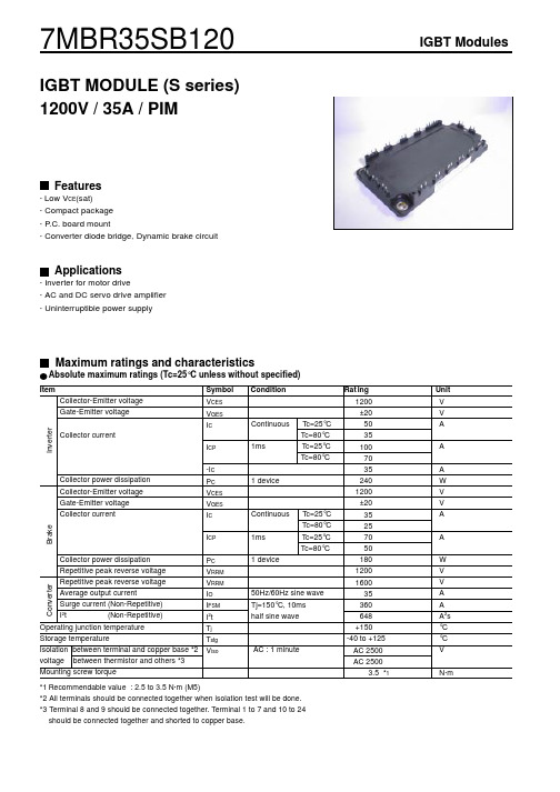
Switching time : ton, tr, toff, tf [ nsec ]
[ Inverter ]
Switching time vs. Collector current (typ.)
Vcc=600V, VGE=±15V, Rg=33Ω, Tj=25°C 1000
500
toff
ton tr
Turn-on time
Turn-off time
Reverse current Forward on voltage
Reverse current Resistance
B value
ICES IGES VGE(th) VCE(sat)
Cies ton tr tr(i) toff tf VF
trr ICES IGES VCE(sat)
20
0 0
8V
1
2
3
4
5
Collector - Emitter voltage : VCE [ V ]
[ Inverter ] Collector-Emitter voltage vs. Gate-Emitter voltage
Tj= 25 oC (typ.) 10
8
6
4 2 0
5
1000
Ic= 70A Ic= 35A Ic= 17.5A
IF=35A
chip
terminal
IF=35A
VCES=1200V, VGE=0V
VCE=0V, VGE=±20V
IC=25A, VGE=15V chip
terminal
VCC=600V
IC=25A
VGE=±15V
RG=51Ω
VR=1200V
实验三七段数码显示译码器设计
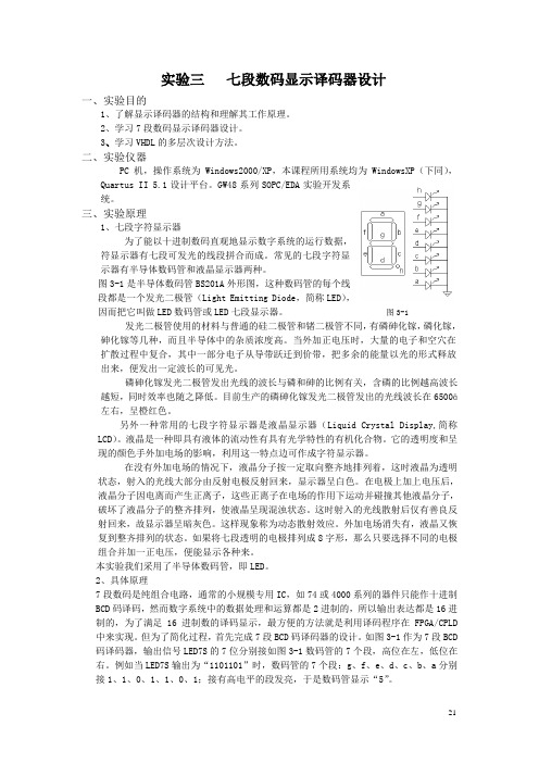
实验三七段数码显示译码器设计一、实验目的1、了解显示译码器的结构和理解其工作原理。
2、学习7段数码显示译码器设计。
3、学习VHDL的多层次设计方法。
二、实验仪器PC机,操作系统为Windows2000/XP,本课程所用系统均为WindowsXP(下同),Quartus II 5.1设计平台。
GW48系列SOPC/EDA实验开发系统。
三、实验原理1、七段字符显示器为了能以十进制数码直观地显示数字系统的运行数据,符显示器有七段可发光的线段拼合而成。
常见的七段字符显示器有半导体数码管和液晶显示器两种。
图3-1是半导体数码管BS201A外形图,这种数码管的每个线段都是一个发光二极管(Light Emitting Diode,简称LED),因而把它叫做LED数码管或LED七段显示器。
图3-1 发光二极管使用的材料与普通的硅二极管和锗二极管不同,有磷砷化镓,磷化镓,砷化镓等几种,而且半导体中的杂质浓度高。
当外加正电压时,大量的电子和空穴在扩散过程中复合,其中一部分电子从导带跃迁到价带,把多余的能量以光的形式释放出来,便发出一定波长的可见光。
磷砷化镓发光二极管发出光线的波长与磷和砷的比例有关,含磷的比例越高波长越短,同时效率也随之降低。
目前生产的磷砷化镓发光二极管发出的光线波长在6500ā左右,呈橙红色。
另外一种常用的七段字符显示器是液晶显示器(Liquid Crystal Display,简称LCD)。
液晶是一种即具有液体的流动性有具有光学特性的有机化合物。
它的透明度和呈现的颜色手外加电场的影响,利用这一特点边可作成字符显示器。
在没有外加电场的情况下,液晶分子按一定取向整齐地排列着,这时液晶为透明状态,射入的光线大部分由反射电极反射回来,显示器呈白色。
在电极上加上电压后,液晶分子因电离而产生正离子,这些正离子在电场的作用下运动并碰撞其他液晶分子,破坏了液晶分子的整齐排列,使液晶呈现混浊状态。
这时射入的光线散射后仅有善良反射回来,故显示器呈暗灰色。
- 1、下载文档前请自行甄别文档内容的完整性,平台不提供额外的编辑、内容补充、找答案等附加服务。
- 2、"仅部分预览"的文档,不可在线预览部分如存在完整性等问题,可反馈申请退款(可完整预览的文档不适用该条件!)。
- 3、如文档侵犯您的权益,请联系客服反馈,我们会尽快为您处理(人工客服工作时间:9:00-18:30)。
s Real-time source level emulation allows viewing and breakpoint setting on high level source code rather than on disassembled target code for optimum user friendliness.
元器件交易网
ST7MDTx-EMU2B
REAL-TIME DEVELOPMENT TOOLS FOR THE ST7 MCU FAMILY
FEATURES
s A common Hardware Development System mainframe supports the entire ST7 family of MCUs, in conjunction with the appropriate ST7xxx-DBE Active Probe.
s 1K by 32-bit wide trace memory allows complex and sequential events to be defined on any combination of address and data, as well as 3 internal and 5 external logic signals.
Log files offer the ability to send any screen display to a text file. In particular, log files are very useful to save the contents of the logic analyzer and/or the contents of data registers to be subsequently analysed or printed.
A separate and concurrent Logic Analyzer function is available. This hardware implemented function features 1KByte of 32-bit wide trace memory which allows events to be defined for any combination of address (16 bits) and data (8 bits), as well as according to the state of 3 internal and 5 external logic signals. Complex and sequential conditions may be defined, and all bits are maskable. The external signals are input from 5 probes which can be connected to the target hardware.
s Special Function Register window - symbolic display of SFR
.
Байду номын сангаас
February 2000
1/4
123
元器件交易网
ST7MDTx-EMU2B
OVERVIEW
The ST7 real-time development tools consist of various hardware and software components, which together form a flexible and sophisticated system designed to provide comprehensive development support for the ST7 family of MCUs.
s 64 KBytes of user modifiable and configurable emulation RAM, allows memory mapping of all ST7 family devices as well as modelling hypothetical memory configurations.
s User defined events may trigger a breakpoint or simply define data capture parameters, in accordance with user preferences.
s Simple connection of the emulator system to the Host PC via parallel port.
The Hardware Development System (HDS) mainframe is common to all ST7 devices and, in conjunction with various active probes, allows emulation and development of specific devices. Only the probe needs to be changed to emulate a new ST7 family device.
s Command files can be used to execute a set of debugger commands in batch mode.
s Editable configuration files ensure tailoring of working environment to user preferences.
An important feature of the ST7 development system is that true source level debugging is possible, meaning code may be viewed at source level and breakpoints may be set on high level code, rather than on disassembled target code. This is much more meaningful to the user and ensures a more convivial and productive development environment.
Once assembled, and/or compiled and linked, the application software may be downloaded to the real-time emulation memory, which can be configured, mapped and modified as required by the user. The device probe is then connected to the application target hardware in place of the MCU and real-time emulation of the target application can begin, thus allowing sophisticated testing and debugging of both application hardware and software.
s Unlimited breakpoints may be set for any opcode fetch or any address access, and conditions may be defined for the generation of 2 external synchronization signals.
The development system is controlled by a Host PC on which a choice of Windows-based software may be run. The Host PC is simply connected to the Emulator Mainframe by means of a parallel port. The STVD7 Windows Debugger software suite is supplied as standard issue with the Emulator hardware, in addition to the conventional DOS ST7 Software suite, which includes a macroassembler, a linker/loader. Third party C Toolchain and Debugger software is also available. The Windows-based debugger provides a user friendly and highly flexible interface which may be configured to precisely match the user’s requirements. All emulator settings are accessible via the control software.