电子信息专业英语7共26页文档
电子信息专业英语要点总结

电子信息专业英语要点总结第一篇:电子信息专业英语要点总结重点词汇1.TDM——Time Division Multiplexing 时分复用FDM CDM 2.PCM——Pulse Code Modulation 脉冲编码调制3.PCI——Peripheral Component Interconnect 周边元件连接口4.IDE——Integrated Drive Electronics 集成驱动器电路5.AGP——Accelerated Graphic Port 加速图形接口B——Universal Serial Bus通用串行接口7.HDL——Hardware Description Language 硬件描述语言8.PLD——Programmable Logic Device 可编程逻辑器件 9.FPGA——Field Programmable Gate Array 现场可编程门阵列 10.ASIC——Application—Specific Integrated Circuit专用集成电路 11.DSP——Digital Signal Processor 数字信号处理器12.SoC——System-on-Chip 片上系统 13.Learnning curve 学习曲线14.IEEE——Institute of Electrical and Electrics Engineers 电气与电子工程师学会15.sample and hold circuit 采样与保持电路16.price/performance ratio 性能价格比 17.harvard architecture 哈佛结构 18.looping scheme 循环机制19.FFT——Fast Fourier transform 快速傅里叶变换 20.PCB——Printed Circuit Board 印刷电路板 21.SPS——Sample Per Second 每秒样本数 22.block diagram 方框图 23.Dolby Stereo 杜比立体声24.transmission bandwidth 传输带宽 25.signal-to-noise ratio 信噪比汉译英句子1.“信道”这个术语通常是指频分多址系统中的一个频率,时分多址系统中的一个时隙,码分多址系统中的一个代码或混合系统中的频率,时隙,代码中的某中组合。
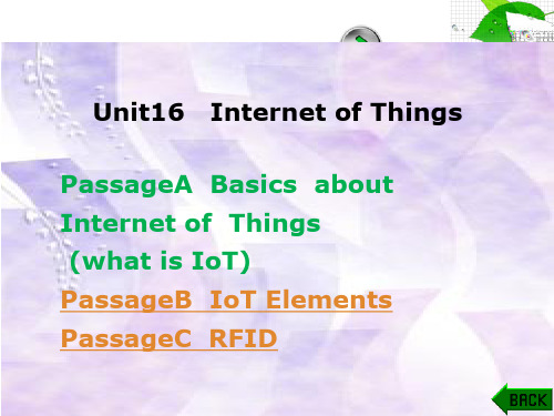
电子信息专业英语——7+unit+16+Internet+of+Things
Unit 4 Microelectronics
Text tour
the IoT’s demands: 物联网需要做如下三个方面: 2. a software architecture and pervasive communication networks to process and convey the contextual information to where it is relevant
3.Create your own slideshow, then embed in your classroom blog. 创建自己的幻灯片, 然后嵌入到教Uni学t 4博Mi客croe中lect.ronics
[3] Fueled by the prevalence of devices enabled by open wireless technology such as Bluetooth, radio frequency identification (RFID), Wi-Fi, and telephonic data services as well as embedded sensor and actuator nodes, IoT has stepped out of its infancy and is on the verge of transforming the current static Internet into a fully integrated Future Internet.
❖ 无线射频技术和传感器网络技术将会成长以满足这一 新的挑战。信息和通信系统以不可见的方式嵌入我们
电子技术专业英语
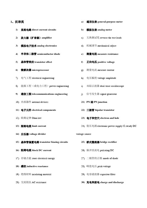
1、汉译英1)直流电路direct current circuits2)放大器(扩音器)amplifier3)模拟电子技术analog electronics4)半导体二极管semiconductor diode5)晶体管效应transistor effect6)微解决器microprocessor7)电气工程electrical engineering8)能源工程(或电力工程)power engineering9)通信工程telecommunications engineering10)内部器件internal devices11)电子元件electrical components12)欧姆定律Ohm law13)限制电流limit current14)分压器voltage divider15)晶体管偏置电路transistor biasing circuits16)阻碍电流block DC current17)存储点能store electrical energy18)感抗inductive reactance19)绝缘材料insulating material20)交流阻抗AC resistancea)通用仪表general-purpose meterb)模拟仪表analog meterc)互换测试笔reverse the test leadsd)机械调节mechanical adjuste)测量电阻measure resistancef)正向电压positive voltageg)测量电流measure currenth)电压幅度voltage amplitudei)双踪示波器dual-trace oscilloscopej)信号发生器signal generator21)PN结PN junction22)三极管bipolar transistor23)电子和空穴electron and hole24)稳压电源electronic power supply或steady DC voltage source25)桥式整流器bridge rectifier26)脉冲直流电pulsating DC27)二极管的正极anode of diode28)峰值电压peak voltage29)电容滤波器capacitor filter30)充电和放电charge and discharge31)稳压管Zener diode32)电器电子工程师学会IEEE(Institute of Electrical and Electronics Engineers)33)专业技术组织technical professional association34)基尔霍夫电压定律Kirchhoff’s V oltage Law35)电压源voltage sources36)电荷守恒定律the law of conservation of electric charge37)在每一瞬时at every instant of time38)元件两端的电压voltages across elements39)无线电传输radio transmission40)频率调制或调频frequency modulation41)频域the frequency domain42)线性电阻linear resistor43)调幅波形amplitude modulation wave44)专用集成电路(ASIC)45)快速时间响应fast response time46)有效信号valid signal47)十进制数字系统decimal system48)逻辑运算logic operation1)控制信号线the control bus2)中断线interrupt lines1)结构化语言structured language2)局部变量local variables3)副作用side effect4)汇编语言指令assembly language instructions1)静止图像still image2)阴极射线管,显像管CRT or the cathode ray tube3)像素pixel4)电子束electron beam2、英译汉1)assembler language汇编语言2)alternating current circuits交流电路3)passive electrical circuits无源电路4)three phase circuits三相电路5)digital electronics数字电子技术6)logic gates逻辑门7)3D virtual reality image三维虚拟图像8)computer programming计算机编程9)major in(在大学里)主修10)advanced programming techniques高级编程技术1)known as capacitive reactance称为容抗2)with units ohms单位为欧姆3)prevent device from burning out防止器件烧掉4)has an AC resistance to AC current对交流电流由阻抗5)adjustment with a screw用一个螺丝调节6)in the shape of a cylinder 呈圆柱形式7)block DC current,but pass AC current阻直流通交流8)to vary the inductance改变电感9)be given by the formula 由公式给出10)the RF amplifier 音频放大器1)analog multimeter模拟万用表2)extended range扩展范围3)specific meters特殊仪表4)includes the function and range switches具有功能及范围选择旋钮5)present an electronic picture呈现一幅电子图像6)display the voltage waveform显示电压波形7)appear on the screen在屏幕上出现8)phase relationships相位关系9)an example例如,作为一个例子10)in series with the circuit串连接入电路1)Semiconductor material半导体材料2)forward biased正向偏置3)depend on the external circuit resistance取决于外部电路的电阻4)excessive reverse-biased voltage过高的反偏电压5)is directly proportional to the amount ofbase current是正比于基极电流6)may even appear almost as a short几乎可当作是短路7)cause stability problems for a transistorcircuit引起晶体管电路的稳定性问题8)digital technology数字技术9)the most popular technology最常用的技术10)use two complementary typeset oftransistors N-channel and P-channel用两种互补型的晶体管——N沟道和P沟道1)equipment operation设备的运营2)device that converts AC into DC把交流电转换成直流电的器件3)the power lines电源线4)depending on the value of DC voltageneeded 根据所需要的直流电压值5) a half-wave rectifier平波整流器6)so as to produce a constant DC output从而产生一个稳定的直流输出7)in the negative side of the capacitor在电容的负极8)flow through the load流过负载9)in the forward-biased condition在加正向偏置电压的条件下10) a series(current-limiting)resistor一个串联(限制电流)电阻1)current source电流源2)under this circumstance在这种情况下3)present the second of Kirchhoff’s laws给出基尔霍夫第二定律4)introduce the concept of a “loop”引入“回路”的概念5)An alternative statement of KVLKVL的另一种表述法6)voltages algebraically sum电压代数和7)sinusoidal steady-syate response正弦稳态响应8)ordinary household voltage平常用电的电压9)time-invariant circuit时不变电路10)percentage of modulation调制比例reduce the power consumption减小消耗功率flip-flop 触发器the octal and hexadecimal systems当时钟脉冲信号来届时改变状态①直流电路direct current circuits②放大器(扩音器)amplifier③欧姆定律Ohm law④正极positive electrode⑤充电与放电Charge and discharge⑥无线电传输Radio transmission⑦模拟仪表Analogue Meters⑧模拟电子技术analog electronics⑨半导体二极管semiconductor⑩晶体管效应transistor effect⑪微解决器microprocessor⑫通信工程telecommunications engineering ⑬汇编语言assembler language⑭电子元件electrical components⑮限制电流limit current⑯分压器voltage divider⑰偏置电路biasing circuits⑱阻碍电流block DC current⑲感抗inductive reactance⑳容抗capacitive21正向电压positive voltage22扩展范围extended range23电压波形voltage waveform24连接入电路in series with the circuit25PN结PN junction 26三极管bipolar transistor27电子与空穴electron and hole28半导体材料semiconductor material29正向偏置forward biased30数字技术digital technology31桥式整流器bridge rectifier32稳压管Zener diode33电源线the power lines34在电容的负极in the negative side of the capacitor 在加正向偏置的条件下in the forward-biased condition一个串联电阻 a series (current-limiting)resistor35电压源voltage sources36在每一瞬时at every instant of time37无线电传输radio transmission38频率调制或调频frequency modulation39快速时间响应fast response time40有效信号valid signal41结构化语言structured language42局部变量local variables43副作用side effect44静止图像still image45阴极射线管pixel 46电子束electron beam1.resistors are used to limit current flowing to adevice ,thereby preventing it from burning out, as voltage dividers to reduce voltage for other circuits, as transistor biasing circuits, and to serve as circuit loads.电阻常用做限流器,限制流过器件的电流防止烧坏器件,电阻也可用作分压器,以减小其他电路电压,还可以用在晶体管偏执电路中和作为电路负载。
电子信息专业英语
被动语态多
科技英语为了避免主观性和个人色彩,常用被动语态。译时可 译为“被”、“经过”、“受了”、“由于“等。 例3 A database may be designed for batch processing, realtime processing, or in-line processing. 例4 If we consider binary transmission, the complete information about a particular message will always be obtained by simply detecting the presence or absence of pulse.
见p16. Anti- 反、防 anti-clockwise anti-corrosive im- 不(后接b,m,p) Imbalance Immovable impossible il-不(后接l) illegal -cy 性质 accuracy -(i)ty 性、度 density possibility ir-不(后接r) irregular
例5 Noise can be introduced into transmission path in many different ways, perhaps via a nearby lighting strike, the sparking of a car ignition system, or the thermal low-level noise within the communication equipment itself. Lighting strike 照明
常用缩写词汇
如AC, A/D,ADC, D/A 等。
专业英语-20070726
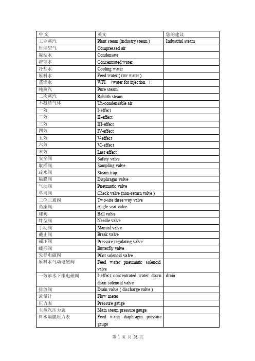
Pilot solenoid valve
Feed water pneumatic solenoid
valve
I-effect concentrated water down drain
drain solenoid valve
Drain valve ( discharge valve ) Flow meter
Pressure gauge
Main steam pressure gauge
Feed water diaphragm pressure
gauge
第 1 页 共 26 页
电导率仪 液位开关 双金属压力表 液位计 静压液位计 调压过滤器 压力控制器 温度传感器 压力变送器 温度变送器 预热器 冷凝器 呼吸器 蒸发器 断路器 过滤器 漏电断路器 接触器 分离器 收集器 换热器 原料水泵 风扇 电机 法兰 螺纹 卡盘 卡箍 清洗球 弯头 封头 垫圈 三通 同心变径 异心变径 三片式卡箍 温度探头 无缝管 有缝管 浮子 人孔 视镜 孔板
Turbidity
Storage tank Mixing tank Stirrer Dish head Ellipse head Burst disc Solep late Impeller Vertical Hor izonta l Baffle plates Stiffening ring Thimble
machine Insulation cladding
第 3 页 共 26 页
蒸汽凝结水排放口 凝结水排放 管程 壳程 列管式 模拟量 数字量 静压液位计 急停开关 料水缓冲罐 地漏 死角 钝化 酸洗 电解抛光 焊接 胀接 降膜式蒸发设备 静压测试 互锁
RO
一级反渗透 二级反渗透 EDI 系统 预处理系统 反渗透主机 一级高压泵 二级高压泵 反渗透膜 膜壳 多介质过滤器 活性炭过滤器 石英砂过滤器 精密过滤器 气动蝶阀 卫生球阀 手动隔膜阀 油膜压力表 PP 棉滤芯 中间水罐 清洗水罐 纯化水罐 清洗水泵
电子信息专业英语

T
N
在国际单位制中,电阻用欧姆来度量。希腊字母 是欧姆的标准符号。较大的电阻一般 SI 国际单位制,英文:International System of Units
ohm 用千欧和兆欧来表示。 n. [物] 欧姆
Text
The circuit element used to model this behavior is the resistor. Figure 1.1 shows the circuit symbol for the resistor, with R denoting the resistance value of the resistor.
Fig.1.2 The circuit symbol for a capacitor
T N
parameter n. 参数,参量 电容的电路参数用字母C表示,用法拉来度量。因为法拉是相当大的电容量,实际上电容值 faradfarad n. [电] 通常位于皮法和微法之间。 法拉,电容单位 picofarad microfarad n. [电] 皮(可), 法拉, 微微法拉, 百亿分之一法拉, 符号为PF或pf n. [电] 微法拉
T
当电流和电压的参考方向关联时,有
di (1.4) dt 这里 v 的单位是伏特,L 的单位是亨利, i 的单位是安培, t 的单位是秒。 v=L
Text
Note from Eq. (1.4) that the voltage across the terminals of an inductor is proportional to the time rate of change of the current in the inductor. We can make two important observations here. First, if the current is constant, the voltage across the ideal inductor is zero. Thus the inductor behaves as a short circuit in the presence of a constant, or dc. current. Second, a current cannot change instantaneously in an inductor, that is, the current cannot change by a finite amount in zero time. An inductor, like a capacitor, stores the energy supplied to it, but it stores energy in the form of a magnetic rather than an electric field.3
电子信息专业英语 (7)
P2口是一个带有内部上拉电阻的8位双向I/O端口。P2的输出缓冲器可驱动(吸收/输出 电流)4个TTL输入。对P2口写“1”时,通过内部上拉电阻把端口拉到高电位,这时可用作 输入口。P2作输入口使用时,因为有内部上拉电阻,那些被外部信号拉低的引脚会输出一 个电流(IIL)。
T N
P1口是一个带有内部上拉电阻的8位双向I/O端口。P1口的输出缓冲器可以驱动4个TTL 输入。当向P1口引脚写“1”时,通过内部的上拉电阻把端口拉到高电位,这时可用作输入 口。作为输入口使用时,由于有内部的上拉电阻,P1被外部信号拉低的引脚将会输出电流 (IIL)。在进行Flash编程和校验时,P1口接收低8位地址。
Company Logo
Text
Port 1 is an 8-bit bi-directional I/O port with internal pull-ups. The Port 1 output buffers can sink/source four TTL inputs. When 1s are written to Port 1 pins, they are pulled high by the internal pull-ups and can be used as inputs. As inputs, Port 1 pins that are externally being pulled low will source current (IIL) because of the internal pull-ups. Port 1 also receives the low-order address bytes during Flash programming and verification.
电子信息专业英语
为了测量电阻,我们使用单位“欧姆”。
To measure resistance,we use the unit "ohm".重要的是要应用这些定律。
It is important to apply these laws. 这种装置能用来测量电流电压电阻。
Such a device can be used to measurecurrent,voltage and resistance. 我们想要求这个电流中的电流。
We wish to find the current in the circuit.无线电波的用途之一是发送信息。
One of the uses of radio waves is to transmit intelligence.在这种情况下该物体被说成带电了。
In this case the object is said to be charged.我们感到理解这个概念很困难。
We find it very difficult to understand this concept.工科学生应该知道如何使用计算机。
Engineering studentsshould know how to use acomputer.物体做工的能力被称为能量。
The ability of a body to do workis called energy.重要的是我们要把理论应用于实践。
It is important for us toapply theory to practice.计算在这个电流中流动的电流密度是可能的。
It is possible tocalculate the current flowing inthis circuit.这些是常用的设备。
These arecommonly used devices.电压等取决于电路中的电阻以及所加的电压。
Voltage equalscurrent multiplied byresistance.显然电流与外加电压成正比。
(完整版)电子信息专业英语复习资料
电子信息专业英语复习资料一、基本术语(英译汉)1.probe探针2.real time operational system 实时操作系统3.debugger 调试器4.sourse code 源代码5.software radio wireless LAN 软件无线电网络6.base station 基站7.top-down approach 自顶向下分析法8.variable 变量9.data compress 数据压缩10.signal conditioning circuit 信号调理电路11.Chebyshev Type Ⅰfilter 切比雪夫Ⅰ型滤波器12.vertical resolution 垂直分辨率13.device driver 设备驱动piler 编译器15.template 模板16.concurrent process 并发进程17.object recognition 目标识别18.Discrete Time Fourier Transform 离散傅立叶变换bined circuit 组合逻辑电路20.impedance transform 阻抗变换器21.voltage source 电压源22.passive component 无源器件23.quality factor 品质因数24.unit-impulse response 单位脉冲响应25.noise origin 噪声源26.Domino effect 多米诺效应27.output load 输出负载28.cordless phone 无绳电话29.Antenna 天线30.harmonic interference 谐波干涉31.Parallel Resonant 并联谐振32.voltage control oscillator 压控振荡器33.adaptive delta modulation 自适应增量调制34.amplitude modulation 调幅二、缩略语(写出全称)1.LSI:large scale integration2.PMOS:p-type metal-oxide semiconductor3.CT:cycle threshold4.MRI:magnetic resonance imaging5.ROM:read-only memory6.DRAM:dynamic random access memory7.TCXO:temperature compensated X'tal (crystal) OscillatorB:Universal Serial Bus9.DCT:discrete cosine transform10.DC:direct current11.CD:Compact Disc12.ASIC:application-specific integrated circuit13.MPEG:Moving Picture Experts Group14.ASSP:application-specific standard product15.EEPROM:electrically erasable programmable read-only memory16.GBW:gain band width17.PLD:programmable-logic device18.RTL:resistor transistor logic19.IP:intellectual property20.FPGA:field-programmable gate array21.CAD:computer-aided design22.MAC:multiply-accmulate23.GSM:Global System for Mobile communications24.CDMA:code division multiple access25.EDA:electronic-design automation26.HDL:hardware-description language27.OS:operating system28.PCB:printed-circuit board29.CMOS:complementary metal-oxide semiconductor30.AC:alternating current31.SRAM:static random-access memory32.PLL:phase-locked loop三、翻译(英译汉+汉译英)1.Bode presented a log technique that transformed the intensely mathematical process of calculating a feedback system's stability into graphical analysis that was simple and perceptive.伯德采用的是一种对数方法——将分析反馈系统稳定性的数学过程转换为简单又好理解的图形化分析。
Integrated_Circuits(集成电路)电子信息类专业英语、计算机类专业英语文章
Integrated Circuits(集成电路)The Integrated CircuitDigital logic and electronic circuits derive their functionality from electronic switches called transistor. Roughly speaking, the transistor can be likened to an electronically controlled valve whereby energy applied to one connection of the valve enables energy to flow between two other connections.By combining multiple transistors, digital logic building blocks such as AND gates and flip-flops are formed. Transistors, in turn, are made from semiconductors. Consult a periodic table of elements in a college chemistry textbook, and you will locate semiconductors as a group of elements separating the metals and nonmetals.They are called semiconductors because of their ability to behave as both metals and nonmetals. A semiconductor can be made to conduct electricity like a metal or to insulate as a nonmetal does. These differing electrical properties can be accurately controlled by mixing the semiconductor with small amounts of other elements. This mixing is called doping. A semiconductor can be doped to contain more electrons (N-type) or fewer electrons (P-type). Examples of commonly used semiconductors are silicon and germanium. Phosphorous and boron are two elements that are used to dope N-type and P-type silicon, respectively.A transistor is constructed by creating a sandwich of differently doped semiconductor layers. The two most common types of transistors, the bipolar-junction transistor (BJT) and the field-effect transistor (FET) are schematically illustrated in Figure 2.1.This figure shows both the silicon structures of these elements and their graphical symbolic representation as would be seen in a circuit diagram. The BJT shown is an NPN transistor, because it is composed of a sandwich of N-P-N doped silicon. When a small current is injected into the base terminal, a larger current is enabled to flow from the collector to the emitter.The FET shown is an N-channel FET, which is composed of two N-type regions separated by a P-type substrate. When a voltage is applied to the insulated gate terminal, a current is enabled to flow from the drain to the source. It is called N-channel, because the gate voltage induces an N-channel within the substrate, enabling current to flow between the N-regions.Another basic semiconductor structure is a diode, which is formed simply by a junction of N-type and P-type silicon. Diodes act like one-way valves by conducting current only from P to N. Special diodes can be created that emit light when a voltage is applied. Appropriately enough, these components are called light emitting diodes, or LEDs. These small lights are manufactured by the millions and are found in diverse applications from telephones to traffic lights.The resulting small chip of semiconductor material on which a transistor or diode is fabricated can be encased in a small plastic package for protection against damage and contamination from the out-side world.Small wires are connected within this package between the semiconductor sandwich and pins that protrude from the package to make electrical contact with other parts of the intended circuit. Once you have several discrete transistors, digital logic can be built by directly wiring these components together. The circuit will function, but any substantial amount of digitallogic will be very bulky, because several transistors are required to implement each of the various types of logic gates.At the time of the invention of the transistor in 1947 by John Bardeen, Walter Brattain, and William Shockley, the only way to assemble multiple transistors into a single circuit was to buy separate discrete transistors and wire them together. In 1959, Jack Kilby and Robert Noyce independently invented a means of fabricating multiple transistors on a single slab of semiconductor material. Their invention would come to be known as the integrated circuit, or IC, which is the foundation of our modern computerized world. An IC is so called because it integrates multiple transistors and diodes onto the same small semiconductor chip. Instead of having to solder individual wires between discrete components, an IC contains many small components that are already wired together in the desired topology to form a circuit.A typical IC, without its plastic or ceramic package, is a square or rectangular silicon die measuring from 2 to 15 mm on an edge. Depending on the level of technology used to manufacture the IC, there may be anywhere from a dozen to tens of millions of individual transistors on this small chip. This amazing density of electronic components indicates that the transistors and the wires that connect them are extremely small in size. Dimensions on an IC are measured in units of micrometers, with one micrometer (1mm) being one millionth of a meter. To serve as a reference point, a human hair is roughly 100mm in diameter. Some modern ICs contain components and wires that are measured in increments as small as 0.1mm! Each year, researchers and engineers have been finding new ways to steadily reduce these feature sizes to pack more transistors into the same silicon area, as indicated in Figure 2.2.When an IC is designed and fabricated, it generally follows one of two main transistor technologies: bipolar or metal-oxide semiconductor (MOS). Bipolar processes create BJTs, whereas MOS processes create FETs. Bipolar logic was more common before the 1980s, but MOS technologies have since accounted the great majority of digital logic ICs. N-channel FETs are fabricated in an NMOS process, and P-channel FETs are fabricated in a PMOS process. In the 1980s, complementary-MOS, or CMOS, became the dominant process technology and remains so to this day. CMOS ICs incorporate both NMOS and PMOS transistors.Application Specific Integrated CircuitAn application-specific integrated circuit (ASIC) is an integrated circuit (IC) customized for a particular use, rather than intended for general-purpose use. For example, a chip designed solely to run a cell phone is an ASIC. In contrast, the 7400 series and 4000 series integrated circuits are logic building blocks that can be wired together for use in many different applications.As feature sizes have shrunk and design tools improved over the years, the maximum complexity (and hence functionality) possible in an ASIC has grown from 5,000 gates to over 100 million.Modern ASICs often include entire 32-bit processors, memory blocks including ROM, RAM, EEPROM, Flash and other large buildingblocks. Such an ASIC is often termed a SoC (System-on-Chip). Designers of digital ASICs use a hardware description language (HDL), such as Verilog or VHDL, to describe the functionality of ASICs.Field-programmable gate arrays (FPGA) are the modern day equivalent of 7400 series logic and a breadboard, containing programmable logic blocks and programmable interconnects that allow the same FPGA to be used in many different applications. For smaller designs and/or lower production volumes, FPGAs may be more cost effective than an ASIC design. The non-recurring engineering cost (the cost to setup the factory to produce a particular ASIC) can run into hundreds of thousands of dollars.The general term application specific integrated circuit includes FPGAs, but most designers use ASIC only for non-field programmable devices and make a distinction between ASIC and FPGAs.HistoryThe initial ASICs used gate array technology. Ferranti produced perhaps the first gate-array, the ULA (Uncommitted Logic Array), around 1980. Customization occurred by varying the metal interconnect mask. ULAs had complexities of up to a few thousand gates. Later versions became more generalized, with different base dies customized by both metal and polysilicon layers. Some base dies include RAM elements.Standard cell designIn the mid 1980s a designer would choose an ASIC manufacturer and implement their design using the design tools available from the manufacturer. While third party design tools were available, there was not an effective link from the third party design tools to the layout and actual semiconductor process performance characteristics of the various ASIC manufacturers.Most designers ended up using factory specific tools to complete the implementation of their designs. A solution to this problem that also yielded a much higher density device was the implementation of Standard Cells. Every ASIC manufacturer could create functional blocks with known electrical characteristics, such as propagation delay, capacitance and inductance; that could also be represented in third party tools.Standard cell design is the utilization of these functional blocks to achieve very high gate density and good electrical performance. Standard cell design fits between Gate Array and Full Custom design in terms of both its NRE (Non-Recurring Engineering) and recurring component cost.By the late 1980s, logic synthesis tools, such as Design Compiler, became available. Such tools could compile HDL descriptions into a gate-level netlist. This enabled a style of design called standard-cell design. Standard-cell Integrated Circuits (ICs) are designed in the following conceptual stages, although these stages overlap significantly in practice.These steps, implemented with a level of skill common in the industry, almost always produce a final device that correctly implements the original design, unless flaws are later introduced by the physical fabrication process.A team of design engineers starts with a non-formal understanding of the required functions for a new ASIC, usually derived from requirements analysis.*The design team constructs a description of an ASIC to achieve these goals using an HDL. This process is analogous to writing a computer program in a high-level language. This is usually called the RTL (register transfer level) design.*Suitability for purpose is verified by simulation. A virtual system created in software, using a tool such as Virtutech’s Simics, can simulate the performance of ASICs at speeds up to billions of simulated instructions per second.*A logic synthesis tool, such as Design Compiler, transforms the RTL design into a large collection of lower-level constructs called standard cells. These constructs are taken from a standard-cell library consisting of pre-characterized collections of gates such as 2 input nor, 2 input nand, inverters, etc.The standard cells are typically specific to the planned manufacturer of the ASIC. The resulting collection of standard cells, plus the needed electrical connections between them, is called a gate-level netlist.*The gate-level netlist is next processed by a placement tool which places the standard cells onto a region representing the final ASIC. It attempts to find a placement of the standard cells, subject to a variety of specified constraints. Sometimes advanced techniques such as simulated annealing are used to optimize placement.*The routing tool takes the physical placement of the standard cells and uses the netlist to create the electrical connections between them. Since the search space is large, this process will produce a “sufficient” rather than “glo bally-optimal” solution. The output is a set of photomasks enabling semiconductor fabrication to produce physical ICs.*Close estimates of final delays, parasitic resistances and capacitances, and power consumptions can then be made. In the case of a digital circuit, this will be further mapped into delay information. These estimates are used in a final round of testing. This testing demonstrates that the device will function correctly over all extremes of the process, voltage and temperature. When this testing is complete the photomask information is released for chip fabrication.These design steps (or flow) are also common to standard product design. The significant difference is that Standard Cell design uses the manufacturer’s cell libraries that have been used in hundreds of other design implementations and therefore are of much lower risk than full custom design.Gate array designGate array design is a manufacturing method in which the diffused layers, i.e. transistors and other active devices, are predefined and wafers containing such devices are held in stock prior to metallization, in other words, unconnected.The physical design process then defines the interconnections of the final device. It is important to the designer that minimal propagation delays can be achieved in ASICs versus the FPGA solutions available in the marketplace. Gate array ASIC is a compromise as mapping a given design onto what a manufacturer held as a stockwafer never gives 100% utilization.Pure, logic-only gate array design is rarely implemented by circuit designers today, replaced almost entirely by field programmable devices such as FPGAs, which can be programmed by the user and thus offer minimal tooling charges, marginally increased piece part cost and comparable performance.Today gate arrays are evolving into structured ASICs that consist of a large IP core like a processor, DSP unit, peripherals, standard interfaces, integrated memories SRAM, and a block of reconfigurable uncommitted logic.This shift is largely because ASIC devices are capable of integrating such large blocks of system functionality and “system on a chip” requires far more than just logic blocks.Full-custom designThe benefits of full-custom design usually include reduced area, performance improvements and also the ability to integrate analog components and other pre-designed components such as microprocessor cores that form a System-on-Chip. The disadvantages can include increased manufacturing and design time, increased non-recurring engineering costs, more complexity in the CAD system and a much higher skill requirement on the part of the design team.However for digital only designs, “standard-cell” libraries together with modern CAD systems can offer considerable performance/cost benefits with low risk. Automated layout tools are quick and easy to use and also offer the possibility to manually optimize any performance limiting aspect of the design.Structured designStructured ASIC design is an ambiguous expression, with different meanings in different contexts. This is a relatively new term in the industry, which is why there is some variation in its definition. However, the basic premise of a structured ASIC is that both manufacturing cycle time and design cycle time are reduced compared to cell-based ASIC by virtue of there being pre-defined metal layers and pre-characterization of what is on the silicon.One definition states that, in a structured ASIC design, the logic mask-layers of a device are predefined by the ASIC vendor (or in some cases by a third party). Structured ASIC technology is seen as bridging the gap between field-programmable gate arrays and “standard-cell” ASIC designs.What makes a structured ASIC different from a gate array is that in a gate array the predefined metal layers serve to make manufacturing turnaround faster. In a structured ASIC the predefined metallization is primarily to reduce cost of the mask sets and is also used to make the design cycle time significantly shorter as well.Likewise, the design tools used for structured ASIC can substantially lower cost, and are easier to use than cell-based tools, because the tools do not have to perform all the functions that cell-based tools do.One other important aspect about structured ASIC is that it allows IP that is comm on to certain applications to be “built in”, rather than “designed in”. By building the IP directly into the architecture the designer can again save both time and money compared to designing IP into a cell-based ASIC.中文翻译:集成电路数字逻辑和电子电路由称为晶体管的电子开关得到它们的(各种)功能。
- 1、下载文档前请自行甄别文档内容的完整性,平台不提供额外的编辑、内容补充、找答案等附加服务。
- 2、"仅部分预览"的文档,不可在线预览部分如存在完整性等问题,可反馈申请退款(可完整预览的文档不适用该条件!)。
- 3、如文档侵犯您的权益,请联系客服反馈,我们会尽快为您处理(人工客服工作时间:9:00-18:30)。
山东信息职业技术学院电子工程系
Text Diode
A diode is a nonlinear electrical device allowing current to move through it in one direction with far greater ease than in the other and usually acting as a one-way valve for current. The most common kind of diode in modern circuit design is the semiconductor diode, although other diode technologies exist. Semiconductor diodes are symbolized in schematic diagrams such as Fig. 2-1.
Oddly enough, the direction of the diode symbol's “arrowhead”points against the direction of electron flow. This is because the diode symbol was invented by engineers, who predominantly use conventional flow notation in their schematics, showing current as a flow of charge from the positive (+) side of the voltage source to the negative (-). This convention holds true for all semiconductor symbols possessing “arrowheads”. The arrow points in the permitted direction of conventional flow, and against the permitted direction of electron flow.
山东信息职业技术学院电子工程系
When the polarity of the battery is such that electrons are allowed to flow through the diode, the diode is said to be forward-biased. Conversely, when the battery is “backward”and the diode blocks current, the diode is said to be reverse-biased. A diode may be thought of as like a switch: “closed” when forward-biased and “open” when reverse-biased. oddly enough:稀奇的是
山东信息职业技术学院电子工程系
New Words and Expressions
diode [ 'daiəud ]
二极管
nonlinear [ nɔn'liniə ]
非线性
-way 单向的
valve [ væ lv ]
阀门
semiconductor [ˌsemikən'dɔktə ]
半导体
schematic [ ski:'mæ tik ]
冶金
silicon [ 'silikən ]
硅
n-type
N型
p-type P型
juxtaposed [ˌ dʒʌkstə'pəuzd ]
紧靠的
ohmmeter [ 'əum ˌ mi:tə ]
欧姆表
qualitatively [ 'kwɔlitətivli]
定性地
purpose
目的
expect
期望
military [ 'militəri ]
军用
civilian [ si'viljən ]
民用
peak [ pi:k ] 峰值
clamper [ 'klæmpə ] 钳子
rectification
整流
photic [ 'fəutik ]
光
decoration [ˌ dekə'reiʃən ]
装潢、装饰
In Fig. 2-1, arrows indicate the direction of electroncurrent flow.
山东信息职业技术学院电子工程系
When placed in a simple battery-lamp circuit, the diode will either allow or prevent current through the lamp, depending on the polarity of the applied voltage. (Fig. 2-2) (a) Current flow is permitted; the diode is forward biased. (b) Current flow is prohibited; the diode is reversed biased.
原理图
symbol [ 'simbəl ]
图表
arrows 箭头
battery [ 'bætəri ]
电源
lamp [ læ mp ]
灯
permit [ pə'mit ]
准许
prohibit [ prəu'hibit ]
禁止
polarity [ pəu'lærəti ]
极性
Conversely
相反
switch [ switʃ ]
开关
oddly [ 'ɔdli ]
奇怪地
invent
发明
山东信息职业技术学院电子工程系
predominantly
占主导地位的
conventional [ kən'venʃənəl ] 习惯的、传统的
notation [ nəu'teiʃən ]
符号、标记
metallurgically [ˌ melə'lə:dʒikli ]