ADL5382ACPZ-WP中文资料
AD538工作原理
摘要:AD538是美国ADI公司出品的单片实时模拟计算芯片,它能实时完成对数、指数、乘方和开方等运算,结构简单、精度高、运算速度快,可在高速工业测控系统、航空航天以及国防领域得到应用。
本文详细地介绍了AD538的原理及应用。
关键词:实时计算;AD5381. 概述AD538是美国ADI公司出品的实时模拟计算器件,能提供精确的模拟乘、除和幂运算功能。
AD538结构独特、工艺精良。
低输入/输出偏移电压和优异的线性性能的结合,使其可在一个非常宽的输入动态范围内进行精确的运算。
激光调整技术可使乘/除运算误差控制在输入幅值的0.25%的范围之内。
通常输出偏移小于或等于100μV。
由于器件具有400kHz带宽,进一步加强了实时模拟信号的处理能力。
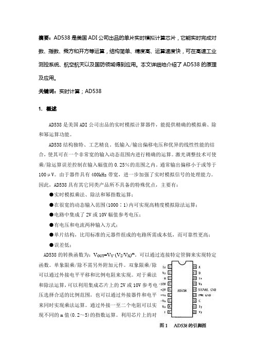
因此,AD538具有其它同类产品所不具备的特殊优点,主要有:●实时模拟乘法、除法和幂指数运算;●在很宽的动态输入范围(1000∶1)内可实现高精度模拟除法运算;●电路中集成了2V或10V幅值参考电压;●有电压和电流两种输入方式;●单片结构,比用标准的元器件组成的电路所需成本低,而可靠性更高;●误差低;AD538的转换函数为:V OUT=V Y·(V Z/V X)m。
可以通过连接特定管脚来实现特定函数。
单象限乘/除不需另外附加元件。
双象限乘/除可以通过外接电平平移和比例电阻来实现。
对于乘法和除法运算,可以利用集成芯片上的2V或10V参考电压选择合适的比例范围,也可以通过外接器件和电平来同时实现乘法运算。
通过外接一至二个电阻可以实现不同的m值(0.2~5)的指数运算。
利用芯片上的对数比例和输出部分可以直接实现对数比例运算。
通过多重的算法连接增加了AD538的灵活性,而且从±4.5到±18V的电源范围内允许选择±5V、±12V和±15V标准电压作为工作时的电源电压。
AD538在-25~+85℃工作温度范围内应用时,有A和B两种精度等级;在军工温度范围内(-55~+125℃)应用时,精度等级为S。
ADI全部产品参考价格

本公司是专业化的电子元器件供应商,具有多年集成电路的销售经验,专业代理ADI公司全线产品,可广泛应用于通讯、汽车、家庭影院、投影电视、消费类音频、计算机和医疗等领域。
我公司所有产品均由美国原厂发货,稳定可靠、可代客订货,并提供免费样品和IC技术咨询服务。
我公司本着交货快捷,价格合理,诚实经营的理念,提供全面周到的配套服务,并在经营中不断完善自我,真诚欢迎新老客户及业界朋友前来咨询,并建立长期友好的合作关系。
如需了解更详细的价格,封装,最小起订量,库存数量,性能,技术参数,替代产品等信息,请访问我公司首页,使用站内搜索工具查询或联系我公司业务代表!公司主页:电话:0662-669217AD790AQ 59.28元/个AD790JN 31.90元/个AD790JNZ 28.94元/个AD790JR 31.90元/个AD790JR-REEL 31.90元/个AD790JR-REEL7 31.90元/个AD790JRZ 28.94元/个AD790JRZ-REEL 28.94元/个AD790JRZ-REEL 728.94元/个AD8561AN 15.05元/个AD8561ANZ 13.88元/个AD8561AR 15.05元/个AD8561AR-REEL 15.05元/个AD8561AR-REEL7 15.05元/个AD8561ARU-REEL 15.05元/个AD8561ARUZ 13.80元/个AD8561ARUZ-REEL 13.80元/个AD8561ARZ 13.80元/个AD8561ARZ-REEL 13.80元/个AD8561ARZ-REEL7 13.80元/个ADAU1513ACPZ 24.57元/个ADAU1513ACPZ-RL 24.57元/个ADAU1513ACPZ-RL7 24.57元/个EVAL-SSM2319Z 389.22元/个EVAL-SSM2335Z 393.90元/个SSM2335CBZ-REEL 4.91元/个SSM2335CBZ-REEL7 4.91元/个EVAL-SSM2335Z 393.90元/个SSM2335CBZ-REEL 4.91元/个SSM2335CBZ-REEL7 4.91元/个AD8564AN 32.06元/个AD8564ANZ 29.09元/个AD8564AR 32.06元/个AD8564AR-REEL 32.06元/个AD8564AR-REEL7 32.06 元/个AD8564ARU-REEL 32.06 元/个AD8564ARUZ-REEL 29.09元/个AD8564ARZ 29.09元/个AD8564ARZ-REEL 29.09 元/个AD8564ARZ-REEL7 元/个 AD8611AR 17.39元/个AD8611AR-REEL 17.39 元/个 AD8611AR-REEL7 17.39元/个 AD8611ARM-R2 17.39元/个AD8611ARM-REEL 17.39 元/个AD8611ARMZ-R2 15.76元/个 AD8611ARMZ-REEL 15.76元/个AD8611ARZ 15.76元/个AD8611ARZ-REEL 15.76元/个AD8611ARZ-REEL7 15.76元/个AD8612ARU 29.25元/个AD8612ARU-REEL 29.25 元/个AD8612ARUZ 26.60元/个AD8612ARUZ-REEL 26.60元/个8600804EA 8600804IA AD96685-REEL AD96685BH AD96685BP AD96685BP-REEL AD96685BQ AD96685BR 26.52元/个AD96685BR-REEL 26.52元/个AD96685BRZ 24.10 元/个AD96685BRZ-REEL 24.10元/个 AD96685TQ/883B 8293G160ARJZ-R2 9.20元/个AD8293G160ARJZ-R7 7.72元/个AD8293G160ARJZ-RL 元/个AD8293G160BRJZ-R2 12.87元/个AD8293G160BRJZ-R7 10.84元/个AD8293G160BRJZ-RL 元/个AD8295ACPZ-R 722.54元/个AD8295ACPZ-RL22.54元/个AD8295ACPZ-WP22.54元/个AD8295BCPZ-R7 33.85元/个AD8295BCPZ-RL 33.85元/个AD8295BCPZ-WP 33.85元/个AD8226ARMZ 元/个AD8226ARMZ-R7元/个AD8226ARMZ-RL 元/个AD8226ARZ元/个AD8226ARZ-R7元/个AD8226ARZ-RL 元/个AD8226BRMZ元/个AD8226BRMZ-R7元/个AD8226BRMZ-RL元/个AD8226BRZ元/个AD8226BRZ-R7元/个AD8226BRZ-RL元/个AD8293G80ARJZ-R2 9.20元/个AD8293G80ARJZ-R7 7.72元/个AD8293G80ARJZ-RL 元/个AD8293G80BRJZ-R2 12.87元/个AD8293G80BRJZ-R7 10.84元/个AD8293G80BRJZ-RL AD202JN 238.99元/个AD202JY 238.99元/个AD202KN 273.23元/个AD202KY 273.23元/个AD203SN 743.65元/个AD204JN 213.41元/个AD204JY213.41元/个AD204KN 247.57元/个AD208BY 585.16元/个AD208BY 666.35元/个AD210AN 418.31元/个AD210BN 503.72元/个AD210JN 375.65元/个AD215AY 384.15元/个AD215BY426.89元/个AD260AND-0 320.42元/个AD260AND-1 320.42元/个AD260AND-2 320.42元/个AD260AND-3 320.42元/个AD260AND-4 320.42元/个AD260AND-5 AD260BND-0 413.40元/个AD260BND-1 413.40元/个AD260BND-2 413.40元/个AD260BND-3 413.40元/个AD260BND-4 413.40元/个AD260BND-5 413.40元/个AD261AND-0 278.38元/个AD261AND-1 278.38元/个AD261AND-2 278.38元/个AD261AND-3 278.38元/个AD261AND-4 278.38元/个AD261AND-5 278.38元/个AD261BND-0 359.19元/个AD261BND-1 359.19元/个AD261BND-2 359.19元/个AD261BND-3 359.19元/个AD261BND-4 359.19元/个AD261BND-5 359.19元/个AD606JN 247.81元/个AD606JNZ 236.96元/个AD606JR 247.81元/个AD606JR-REEL7 247.81元/个AD606JRZ 236.96元/个AD606JRZ-REEL7 236.96元/个5962-9095501M2A8334AC114.35元/个AD8334ACPZ-REEL 114.35元/个AD8334ACPZ-REEL7 114.35元/个AD8335-EVALZ 2294.68元/个AD8335ACPZ 94.69元/个AD8335ACPZ-REEL 94.69元/个AD8335ACPZ-REEL7 94.69元/个AD8336-EVALZ 710.03元/个AD8336ACPZ-R7 36.27元/个AD8336ACPZ-RL35.80元/个AD8336ACPZ-WP 36.27元/个AD8337-EVALZ 642.56元/个AD8337-EVALZ-INV1055.57元/个AD8337-EVALZ-SS 1468.58元/个AD8337BCPZ-R2 19.66元/个AD8337BCPZ-REEL AD8337BCPZ-REEL7 19.66元/个AD8337BCPZ-WP 19.66元/个AD8350AR15 21.61元/个AD8350AR15-EVAL 781.48元/个AD8350AR15-REEL7 21.61元/个AD8350AR20 21.61元/个AD8350AR20-EVAL 781.48元/个AD8350AR20-REEL7 21.61元/个AD8350ARM15 21.61元/个AD8350ARM15-REEL7 21.61元/个AD8350ARM20 21.61元/个AD8350ARM20-REEL7 21.61元/个AD8350ARMZ15 19.66元/个AD8350ARMZ15-REEL7 19.66元/个AD8350ARMZ20 19.66元/个AD8350ARMZ20-REEL719.66元/个AD8350ARZ15-REEL7 19.66元/个AD8350ARZ20-REEL7 19.66元/个AD8351-EVALZ 781.48元/个AD8351ARM 23.09元/个AD8351ARM-REEL7 23.09元/个AD8351ARMZ 20.90元/个AD8351ARMZ-REEL7 20.90元/个AD8352-EVALZ 781.48元/个AD8352ACPZ-R2 AD8352ACPZ-R7 27.54 元/个AD8352ACPZ-WP 27.54元/个AD8366ACPZ-R7 AD8367-EVALZ AD8367ARU 39.55元/个AD8367ARU-REEL7 39.55元/个AD8367ARUZ 35.88元/个AD8367ARUZ-RL7 35.88元/个AD8368-EVALZ 781.48元/个AD8368ACPZ-REEL7 35.88元/个AD8368ACPZ-WP 35.88元/个AD8369-EVALZ 781.48元/个AD8369ARU 36.50元/个AD8369ARU-REEL7 36.50元/个AD8369ARUZ 33.15元/个AD8369ARUZ-REEL7 33.15元/个AD8370-EVALZ AD8370ARE 36.50元/个AD8370ARE-REEL7 36.50元/个AD8370AREZ 33.15元/个AD8370AREZ-RL7 33.15元/个AD8372-EVALZ AD8372ACPZ-R2 AD8372ACPZ-R7 51.32元/个AD8372ACPZ-WP 71.06元/个AD8375-EVALZ AD8375ACPZ-R7 35.41元/个AD8375ACPZ-WP 35.41元/个AD8376-EVALZ AD8376ACPZ-R7 51.25元/个AD8376ACPZ-WP 51.25元/个ADL5330-EVALZ 781.48元/个ADL5330ACPZ-R2 39.31元/个ADL5330ACPZ-REEL7 39.31元/个ADL5330ACPZ-WP 39.31元/个ADL5390-EVALZ 1560.00元/个ADL5390ACPZ-REEL7 59.20元/个ADL5390ACPZ-WP 59.20元/个ADL5391-EVALZ 1578.72元/个ADL5391ACPZ-R2 38.61元/个ADL5391ACPZ-R7 38.61元/个ADL5391ACPZ-WP 38.61元/个ADL5592-EVALZ ADL5592ACPZ-R7元/个ADA4859-3ACPZ-R2 15.52元/个ADA4859-3ACPZ-R7 15.52元/个ADA4859-3ACPZ-RL 15.52元/个ADA4856-3YCPZ-R2 12.79元/个ADA4856-3YCPZ-R7 10.84元/个ADA4856-3YCPZ-RL 10.84元/个ADA4420-6ARQZ 5.38元/个ADA4420-6ARQZ-R7 5.38元/个ADA4420-6ARQZ-RL 5.38元/个ADA4420-6ARUZ 元/个ADA4420-6ARUZ-R7元/个ADA4420-6ARUZ-R元/个AD800-52BR 184..16元/个AD800-52BRRL 元/个AD800-52BRZ 165.44元/个AD800-52BRZRL元/个AD60003RSZ24 AD60003RSZ24RL7元/个AD807A-155BR 108.89元/个AD807A-155BRRL 108.89元/个AD807A-155BRRL7 108.89元/个AD807A-155BRZ 98.98元/个AD807A-155BRZRL98.98元/个AD807A-155BRZRL7 98.98元/个AD60007 AD808-622BR 110.84元/个AD808-622BRRL AD808-622BRZ 100.70元/个AD808-622BRZRL7 ADN2804ACPZ 78.00元/个ADN2804ACPZ-500RL7 78.00元/个ADN2804ACPZ-RL7 78.00元/个EVAL-ADN2804EB 4538.82元/个ADN2805ACPZ 72.77元/个ADN2805ACPZ-500RL7 72.77元/个ADN2805ACPZ-RL7 72.77元/个EVAL-ADN2805EBZ 4538.82元/个ADN2806ACPZ 72.07元/个ADN2806ACPZ-500RL7 72.07元/个ADN2806ACPZ-RL7 72.07元/个EVAL-ADN2806EB 4538.82元/个ADN2807ACP 99.84元/个ADN2807ACPZ 90.79元/个ADN2807ACPZ-RL 90.79元/个EVAL-ADN2807-CML 4538.82元/个ADN2811ACP-CML292.03元/个ADN2811ACP-CML-RL292.03元/个ADN2811ACPZ-CML 292.03元/个EVAL-ADN2811-CML ADN2812ACP 468.86元/个ADN2812ACP-RL7 468.86元/个ADN2812ACPZ 426.27元/个ADN2812ACPZ-RL426.27元/个ADN2812ACPZ-RL7 426.27元/个EVAL-ADN2812-U2 EVAL-ADN2812EBZ 4538.92元/个ADN2813ACPZ 153.89元/个ADN2813ACPZ-500RL7 153.89元/个ADN2813ACPZ-RL7 153.89元/个EVAL-ADN2813EB 4538.82元/个ADN2814ACPZ 90.79元/个ADN2814ACPZ-500RL7 90.79元/个ADN2814ACPZ-RL7 90.79元/个EVAL-ADN2814EB 4538.82 元/个ADN2815ACPZ 138.53元/个ADN2815ACPZ-500RL7 138.53元/个ADN2815ACPZ-RL7 138.53元/个EVAL-ADN2815EB 4538.82元/个ADN2816ACPZ 83.15元/个ADN2816ACPZ-500RL7 93.91元/个ADN2816ACPZ-RL7 81.67元/个EVAL-ADN2816EB4538.82元/个ADN2817ACPZ 345.23元/个ADN2817ACPZ-RL ADN2817ACPZ-RL7 345.23元/个EVAL-ADN2817EB EVAL-ADN2817EBZ ADN2818ACPZ327.99元/个ADN2818ACPZ-RL ADN2818ACPZ-RL7 327.99元/个ADN2819ACP-CML390.70元/个ADN2819ACP-CML-RL 390.70元/个ADN2819ACPZ-CML355.21元/个ADN2819ACPZ-CML-RL 355.21元/个EVAL-ADN2819-CML AD9510-VCO/PCB AD9510-VCO/PCBZ 1184.04元/个AD9510/PCB AD9510/PCBZ 1184.04元/个AD9510BCPZ 94.30元/个AD9510BCPZ-REEL7 94.30元/个AD9511-VCO/PCB AD9511/PCB AD9511/PCBZ AD9511BCPZ 78.55元/个AD9511BCPZ-REEL7 78.55元/个AD9512/PCB 789.36元/个AD9512BCPZ 70.67元/个AD9512BCPZ-REEL7 70.67 元/个AD9513/PCB 786.70元/个AD9513/PCBZ 786.70元/个AD9513BCPZ 46.96元/个AD9513BCPZ-REEL7 46.96元/个AD9514/PCB 986.70元/个AD9514/PCBZ 986.70元/个AD9514BCPZ 46.96元/个AD9514BCPZ-REEL7 46.96元/个AD9515/PCB 986.70元/个AD9515/PCBZ 986.70元/个AD9515BCPZ 37.52元/个AD9515BCPZ-REEL7 37.52元/个AD9516-0/PCBZ 986.70元/个AD9516-0BCPZ 98.67元/个AD9516-0BCPZ-REEL7 98.67元/个AD9516-0/PCBZ 986.70元/个AD9516-0BCPZ 98.67 元/个AD9516-0BCPZ-REEL7 98.67元/个AD9516-1/PCBZ 986.70元/个AD9516-1BCPZ 98.67元/个AD9516-1BCPZ-REEL7 98.67元/个AD9516-2/PCBZ 986.70元/个AD9516-2BCPZ 98.67元/个AD9516-2BCPZ-REEL7 98.67元/个AD9516-3/PCBZ 986.70元/个AD9516-3BCPZ 98.67元/个AD9516-3BCPZ-REEL7 98.67元/个AD9516-4/PCBZ 986.70元/个AD9516-4BCPZ 98.67元/个AD9516-4BCPZ-REEL7 98.67元/个AD9517-0/PCBZ 986.70元/个AD9517-0BCPZ 90.01元/个AD9517-0BCPZ-REEL7 90.01元/个AD9517-1/PCBZ 986.70元/个AD9517-1BCPZ 90.01元/个AD9517-1BCPZ-REEL7 90.01元/个AD9517-2/PCBZ 986.70元/个AD9517-2BCPZ 90.01元/个AD9517-2BCPZ-REEL7 90.01元/个AD9517-3/PCBZ 986.70元/个AD9517-3BCPZ 90.01元/个AD9517-3BCPZ-REEL7 90.01元/个AD9517-4/PCBZ986.70元/个AD9517-4BCPZ 90.01元/个AD9517-4BCPZ-REEL7 90.01元/个AD9518-0/PCBZ 986.70元/个AD9518-0BCPZ 77.77元/个AD9518-0BCPZ-REEL7 77.77元/个AD9518-1/PCBZ 986.70元/个AD9518-1BCPZ 77.77元/个AD9518-1BCPZ-REEL7 77.77元/个AD9518-2/PCBZ 986.70元/个AD9518-2BCPZ 77.77元/个AD9518-2BCPZ-REEL7 77.77元/个AD9518-3/PCBZ 986.70元/个AD9518-3BCPZ 77.77元/个AD9518-3BCPZ-REEL7 77.77元/个AD9518-4/PCBZ 986.70元/个AD9518-4BCPZ 77.77元/个AD9518-4BCPZ-REEL7 77.77元/个AD9522-0/PCBZ元/个AD9522-0BCPZ 98.67元/个AD9522-0BCPZ-REEL7 98.67元/个AD9540-VCO/PCB 197.34元/个AD9540-VCO/PCBZ 197.34元/个AD9540/PCB 197.34元/个AD9540/PCBZ 197.34元/个AD9540BCPZ 78.55元/个AD9540BCPZ-REEL7 78.55元/个AD9549/PCBZ 986.70元/个AD9549BCPZ 97.97元/个AD9549BCPZ-REEL7 97.97元/个ADCLK905/PCBZ 986.70元/个ADCLK905BCPZ-R2 44.23元/个ADCLK905BCPZ-R7 44.23元/个ADCLK905BCPZ-WP 44.23元/个ADCLK907/PCBZ 986.70元/个ADCLK907BCPZ-R2 53.27元/个ADCLK907BCPZ-R7 53.27元/个ADCLK907BCPZ-WP 53.27元/个ADCLK925/PCBZ 986.70元/个ADCLK925BCPZ-R2 46.96元/个ADCLK925BCPZ-R7 46.96元/个ADCLK925BCPZ-WP 46.96元/个AD1955ARS 元/个AD1955ARSRL 元/个AD1955ARSZ 59.20元/个AD1955ARSZRL元/个EVAL-AD1955EBZ 3749.46元/个AD1853JRS元/个AD1853JRSRL元/个AD1853JRSZ 71.06元/个AD1853JRSZRL元/个AD1852JRSZ 63.18元/个AD1852JRSZRL AD1854JRS 52.10元/个AD1854JRSRL AD1854JRSZ 47.35元/个AD1854JRSZRL AD1854KRS 59.20元/个AD1854KRSRL元/个AD1933YSTZ 28.55元/个AD1933YSTZ-RL28.55元/个AD1833AASTZ 59.20元/个AD1833AASTZ-REEL元/个AD1833ACSTZ 34.32元/个AD1934YSTZ 24.57元/个AD1934YSTZ-RL 24.57元/个AD1851N AD1851N-J AD1851NZ AD1851NZ-J AD1851RAD1851R-J AD1851R-REEL7 AD1851RZ 55.07元/个AD1851RZ-J 59.20元/个AD1851RZ-REEL7 AD1859JR AD1859JR-REEL 56.16元/个AD1859JRS AD1859JRS-REEL56.16元/个AD1859JRZ AD1859JRZ-RL AD1866N AD1866NZ AD1866R AD1866R-REEL AD1866RZ 91.18元/个AD1866RZ-REEL AD5337ARM 9.59元/个AD5337ARM-REEL7 9.59元/个AD5337ARMZ 8.74元/个AD5337ARMZ-REEL7 8.74元/个AD5337BRM AD5337BRM-REEL 12.32元/个AD5337BRM-REEL7 12.32元/个AD5337BRMZ 12.32元/个AD5337BRMZ-REEL 12.32元/个AD5337BRMZ-REEL7 12.32元/个5962-9090801M2ADP2108ACPZ-2.3-R7 ADP2108ACPZ-2.5-R7 ADP2108ACPZ-3.0-R7 ADP2108ACPZ-3.3-R7 ADP2108AUJZ-1.0-R7 ADP2108AUJZ-1.1-R7 ADP2108AUJZ-1.2-R7 ADP2108AUJZ-1.3-R7 ADP2108AUJZ-1.5-R7 ADP2108AUJZ-1.8-R7 ADP2108AUJZ-1.82R7 ADP2108AUJZ-2.3-R7 ADP2108AUJZ-2.5-R7 ADP2108AUJZ-3.0-R7 ADP2108AUJZ-3.3-R7 ADP130-0.8-EVALZ 468.00元/个ADP1752-1.5-EVALZ 468.00元/个ADP1752ACPZ-0.75R7 7.02元/个ADP1752ACPZ-1.0-R7 7.02元/个ADP1752ACPZ-1.1-R7 7.02元/个ADP1752ACPZ-1.2-R7 7.02元/个ADP1752ACPZ-1.5-R7 7.02元/个ADP1752ACPZ-1.8-R7 7.02元/个ADP1752ACPZ-2.5-R7 7.02元/个ADP1753-EVALZ ADP1753ACPZ-R7 7.02元/个ADP1754-1.5-EVALZ 468.00元/个ADP1754ACPZ-0.75R7 7.41元/个ADP1754ACPZ-1.0-R7 7.41元/个ADP1754ACPZ-1.1-R7 7.41元/个ADP1754ACPZ-1.2-R7 7.41元/个ADP1754ACPZ-1.5-R7 7.41 元/个ADP1754ACPZ-1.8-R7 7.41元/个ADP1754ACPZ-2.5-R7 7.41元/个ADP1755-EVALZ ADP1755ACPZ ADP1755ACPZ-R7 7.41元/个ADP1740-1.5-EVALZ ADP1740-BL1-EVZADP1740 ACPZ-0.75R7 9.36元/个ADP1740ACPZ-1.0-R7 9.36元/个ADP1740ACPZ-1.1-R7 9.36元/个ADP1740ACPZ-1.2-R7 9.36元/个ADP1740ACPZ-1.5-R7 9.36元/个ADP1740ACPZ-1.8-R7 9.36元/个ADP1740ACPZ-2.5-R7 9.36元/个ADP1741-EVALZ ADP1741ACPZ ADP1741ACPZ-R7 ADP120-12-EVALZ 468.00元/个ADP120-15-EVALZ 468.00元/个ADP120-18-EVALZ 468.00元/个ADP120-33-EVALZ 468.00元/个ADP120-ACBZ12R7 2.26元/个ADP120-ACBZ155R7 ADP120-ACBZ15R7 2.26 元/个ADP120-ACBZ165R7 ADP120-ACBZ16R7 ADP120-ACBZ175R7 ADP120-ACBZ17R7 ADP120-ACBZ188R7 ADP120-ACBZ18R7 2.26元/个ADP120-ACBZ25R7 2.26元/个ADP120-ACBZ278R7 ADP120-ACBZ28R7元/个ADP120-ACBZ29R7 元/个ADP120-ACBZ33R7 ADP120-AUJZ12R7 2.03元/个元ADP120-AUJZ15R7 2.03/个ADP120-AUJZ18R7 2.03元/个ADP120-AUJZ33R7 2.03元/个ADP120-BL1-EVZ 78.00元/个ADP120CB-1.2-EVALZ ADP120CB-1.5-EVALZ ADP120CB-1.8-EVALZ ADP120CB-2.5-EVALZ ADP120CB-2.8-EVALZ ADP121-2.8-EVALZ ADP121-3.0-EVALZ 468.00元/个ADP121-3.3-EVALZ ADP121-ACBZ12R7ADP121-ACBZ155R7ADP121-ACBZ15R7ADP121-ACBZ165R7ADP121-AC BZ16R7 ADP121-ACBZ175R7 ADP121-ACBZ17R7 ADP121-ACBZ188R7 ADP121-ACBZ18R7 2.42元/个ADP121-ACBZ20R7 2.42元/个ADP121-ACBZ25R7 ADP121-ACBZ278R7 ADP121-ACBZ28R7 2.42元/个ADM1184ARMZ18.88元/个ADM1184ARMZ-REEL7 18.88元/个EVAL-ADM1184EBZ ADM1810-10AKS-RL7 3.98元/个ADM1810-10AKSZ-RL 3.59元/个ADM1810-10AKSZ-RL7 3.59元/个ADM1810-10ART-RL7 3.98元/个ADM1810-10ARTZ-RL 3.59元/个ADM1810-10ARTZ-RL7 3.59元/个ADM1810-5AKSZ-REEL 3.59元/个ADM1810-5AKSZ-RL7 3.59元/个ADM1810-5ART-REEL7 3.98 元/个ADM1810-5ARTZ-REEL 3.59元/个ADM1810-5ARTZ-RL7 ADM1811-10AKS-RL7 4.37元/个ADM1811-10AKSZ-RL ADM1811-10AKSZ-RL7 3.98元/个ADM1811-10ART-REEL 3.98元/个ADM1811-10ART-RL7 3.98元/个ADM1811-10ARTZ-RL 3.59元/个ADM1811-10ARTZ-RL7 3.59元/个ADM1811-5AKS-RL7 4.37元/个ADM1811-5AKSZ-REEL ADM1811-5AKSZ-RL7 3.98元/个ADM1811-5ART-REEL ADM1811-5ART-REEL7 3.98元/个ADM1811-5ARTZ-REEL ADM1811-5ARTZ-RL7 3.59元/个ADM1812-10AKS-RL7 4.37元/个ADM1812-10AKSZ-RL 3.98元/个ADM1812-10AKSZ-RL7 3.98元/个ADM1812-10ART-RL7 3.98元/个ADM1812-10ARTZ-RL 3.59元/个ADM1812-10ARTZ-RL7 3.59元/个ADM1812-5AKS-RL7 4.37元/个ADM1812-5AKSZ-REEL ADM1812-5AKSZ-RL7 3.98元/个ADM1812-5ART-REEL7 3.98元/个ADM1812-5ARTZ-REEL 3.59元/个ADM1812-5ARTZ-RL7 3.59元/个ADM1813-10AKS-REEL 3.43元/个ADM1813-10AKS-RL7 3..43元/个ADM1813-10AKSZ-RL 3.04元/个ADM1813-10AKSZ-RL7 3.04元/个ADM1813-10ART-REEL 3.43 元/个ADM1813-10ART-RL7 3.43元/个ADM1813-10ARTZ-RL 3.04元/个ADM1813-10ARTZ-RL7 3.04元/个ADM1813-5AKS-REEL 3.73元/个ADM1813-5AKS-RL7 3.73元/个ADM1813-5AKSZ-REEL 3.04元/个ADM1813-5AKSZ-RL7 3.04元/个ADM1813-5ART-RL7 3.43 元/个ADM1813-5ART-U1 ADM1813-5ARTZ-RL 3.04元/个ADM1813-5ARTZ-RL7 3.04元/个ADM1815-10AKS-RL7 ADM1815-10AKSZ-RL3.82元/个ADM1815-10AKSZ-RL7 3.51元/个ADM1815-10ART-REEL 3.51元/个ADM1815-10ART-RL7 ADM1815-10ARTZ-RL 3.43元/个ADM1815-10ARTZ-RL7 ADM1815-20AKSZ-RL3.51元/个ADM1815-20AKSZ-RL7 3.51元/个ADM1815-20ART-RL7 ADM1815-20ARTZ-RL7 ADM1815-5AKS-RL7 3.51元/个ADM1815-5AKSZ-REEL 3.51 元/个ADM1815-5AKSZ-RL7 ADM1815-5ART-REEL7 3.43元/个ADM1815-5ARTZ-REEL 3.04元/个ADM1815-R22AKSZ-R7 3.82元/个ADM1815-R22AKSZ-RL 3.51 元/个ADM1815-R22ART-RL7 3.43元/个ADM1815-R22ARTZ-R7 3.04元/个ADM1815-R22ARTZ-RL 3.04元/个ADM1815-R23AKSZ-R7 3.82元/个ADM1816-10AKSZ-RL3.98元/个ADM1816-10AKSZ-RL7 3.98 元/个ADM1816-10ART-REEL 3.98元/个ADM1816-10ART-RL7 3.98元/个ADM1816-10ARTZ-RL 3.59元/个ADM1816-10ARTZ-RL7 3.59元/个ADM1816-20AKS-RL7 3.98元/个ADM1816-20AKSZ-RL 3.59元/个ADM1816-20AKSZ-RL7 3.98元/个ADM1816-20ART-RL7 3.98元/个ADM1816-20ARTZ-RL 3.59元/个ADM1816-20ARTZ-RL7 3.59元/个ADM1816-5AKS-REEL7 3.98元/个ADM1816-5AKSZ-REEL 3.90 元/个ADM1816-5AKSZ-RL7 3.90元/个ADM1816-5ART-REEL7 3.59 元/个ADM1816-5ARTZ-REEL 3.59 元/个ADM1816-5ARTZ-RL7 3.59元/个ADM1816-R22AKS-RL7 4.37元/个ADM1816-R22AKSZ-R7 3.98 元/个ADM1816-R22AKSZ-RL3.98元/个ADM1816-R22ART-RL7 3.98元/个ADM1816-R22ARTZ-R7 3.59元/个ADM1816-R22ARTZ-RL 3.59元/个ADM1816-R23AKSZ-R7 ADM1816-R23AKSZ-RL3.98元/个ADM1816-R23ART-RL7 3.98元/个ADM1816-R23ARTZ-R7 3.59元/个ADM1816-R23ARTZ-RL 3.59 元/个ADM1817-10AKS-RL7 4.37元/个ADM1817-10AKSZ-RL 3.98 元/个ADM1817-10AKSZ-RL7 3.98元/个ADM1817-10ART-REEL 3.98元/个ADM1817-10ART-RL7 3.98元/个ADM1817-10ARTZ-RL3.59元/个ADM1817-10ARTZ-RL7 3.59元/个ADM1817-20AKS-RL7 ADM1817-20AKSZ-RL3.98元/个ADM1817-20AKSZ-RL7 3.98元/个ADM1817-20ART-RL7 ADM1817-20ARTZ-RL3.59元/个ADM1817-20ARTZ-RL7 3.59元/个ADM1817-5AKSZ-REEL 3.90元/个ADM1817-5AKSZ-RL7 3.90元/个ADM1817-5ART-REEL7 3.59元/个ADM1817-5ARTZ-REEL 3.59元/个ADM1817-5ARTZ-RL7 3.59元/个ADM1817-R22AKS-RL ADM1817-R22AKSZ-R7 3.90元/个ADM1817-R22AKSZ-RL 3.90元/个ADM1817-R22ART-RL7 3.59元/个ADM1817-R22ARTZ-R7 3.59元/个ADM1817-R22ARTZ-RL 3.59元/个ADM1817-R23AKS-RL ADM1817-R23AKSZ-R7 3.98元/个ADM1817-R23AKSZ-RL 3.98元/个ADM1817-R23ART-RL7 3.98元/个ADM1817-R23ARTZ-R7 3.59元/个ADM1817-R23ARTZ-RL 3.59元/个ADM1818-10AKS-RL7 ADM1818-10AKSZ-RL 3.59 元/个ADM1818-10AKSZ-RL7 3.59元/个ADM1818-10ARTZ-RL7 3.51元/个ADM1818-20AKSZ-RL ADM1818-20AKSZ-RL7 ADM1818-20ART-REEL 3.98元/个ADM1818-20ART-RL7 3.98元/个ADM1818-20ARTZ-RL7 3.98元/个ADM1085AKS-REEL7 2.89元/个ADM1085AKSZ-REEL7 3.65元/个ADM1086AKS-REEL7 2.89元/个ADM1086AKS-U1 ADM1086AKSZ-REEL7 2.65元/个ADM1087AKS-REEL7 2.89元/个ADM1087AKSZ-REEL7 2.65元/个EVAL-ADM1087EBZ 1184.04 元/个ADM1088AKSZ-REEL7 ADM1184ARMZ 18.88元/个ADM1184ARMZ-REEL7 18.88元/个EVAL-ADM1184EBZ ADM1185ARMZ-1 9.44元/个ADM1185ARMZ-1REEL7 9.44元/个EVAL-ADM1185EBZ 1184.04元/个ADM1186-1ARQZ 30.03元/个ADM1186-1ARQZ-REEL 30.03元/个ADM1186-2ARQZ 23.56元/个ADM1186-2ARQZ-REEL23.56元/个EVAL-ADM1186-1EBZ 1262.98元/个EVAL-ADM1186-1MBZ 236.81元/个EVAL-ADM1186-2EBZ 1262.98元/个EVAL-ADM1186-2MBZ 236.81元/个ADM6819ARJZ-REEL7 9.44元/个ADM6820ARJZ-REEL7 9.44元/个ADM1060ARU 56.47 元/个ADM1060ARU-REEL 56.47元/个ADM1060ARU-REEL7 56.47元/个ADM1060ARUZ 51.32元/个ADM1060ARUZ-REEL751.32元/个EVAL-ADM1060EBZ 1973.40元/个ADM1062ACP 65.13元/个ADM1062ACPZ 71.06元/个ADM1062ACPZ-REEL7 71.06元/个ADM1062ASU 65.13元/个ADM1062ASUZ 59.20元/个ADM1062ASUZ-REEL7 59.20元/个EVAL-ADM1062LFEBZ 2368.08元/个EVAL-ADM1062TQEBZ 2368.08元/个ADM1063ACP 71.68 元/个ADM1063ACPZ 65.13元/个ADM1063ACPZ-REEL7 65.13元/个ADM1063ASU 71.68元/个ADM1063ASUZ 65.13元/个ADM1063ASUZ-REEL7 65.13元/个EVAL-ADM1063LFEBZ 2368.08元/个EVAL-ADM1063TQEBZ 2368.08元/个ADM1064ACP 67.31元/个ADM1064ACP-REEL 67.31元/个ADM1064ACP-REEL7 67.31元/个ADM1064ACPZ 61.07元/个ADM1064ASU 67.31元/个ADM1064ASU-REEL 67.31元/个ADM1064ASU-REEL7 67.31元/个ADM1064ASUZ 61.15元/个EVAL-ADM1064LFEBZ 2604.89元/个EVAL-ADM1064TQEBZ 2368.08元/个ADM1065ACP49.50元/个ADM1065ACP-REEL7 49.50元/个ADM1065ACPZ 45.40元/个ADM1065ASU49.50元/个ADM1065ASU-REEL7 49.50元/个ADM1065ASUZ 45.40元/个EVAL-ADM1065LFEBZ 2368.08元/个EVAL-ADM1065TQEBZ 2368.08元/个ADM1066ACP 73.79元/个ADM1066ACP-REEL 73.79元/个ADM1066ACP-REEL7 73.79元/个ADM1066ACPZ 67.08元/个ADM1085AKS-REEL7 2.89元/个ADM1085AKSZ-REEL7 2.65元/个ADM1086AKS-REEL7 2.89元/个ADM1086AKS-U1 ADM1086AKSZ-REEL7 2.65元/个ADM1087AKS-REEL7 2.89 元/个ADM1087AKSZ-REEL7 2.65元/个EVAL-ADM1087EBZ 1184.04元/个ADM1184ARMZ 18.88元/个ADM1184ARMZ-REEL7 18.88元/个EVAL-ADM1184EBZ ADM1185ARMZ-1 9.44元/个ADM1185ARMZ-1REEL7 9.44元/个EVAL-ADM1185EBZ 1184.04元/个ADM1186-1ARQZ 30.03元/个ADM1186-1ARQZ-REEL 30.03元/个ADM1186-2ARQZ 23.57元/个ADM1186-2ARQZ-REEL 23.57元/个EVAL-ADM1186-1EBZ 1262.98元/个EVAL-ADM1186-1MBZ 236.81元/个EVAL-ADM1186-2EBZ 1262.98元/个EVAL-ADM1186-2MBZ 236.81元/个ADM1185ARMZ-1 9.44元/个ADM1185ARMZ-1REEL7 9.44元/个EVAL-ADM1185EBZ 1184.04元/个ADM1186-1ARQZ 30.03元/个ADM1186-1ARQZ-REEL 30.03元/个ADM1186-2ARQZ ADM802LARN 20.83元/个ADM802LARNZ 18.95元/个ADM802LARNZ-REEL ADM802MAN ADM802MANZ 18.95 元/个ADM802MARN 20.83元/个ADM802MARNZ18.95元/个ADM805LAN20.83元/个ADM805LANZ 18.95元/个ADM805LARN20.83元/个ADM805LARNZ 18.95 元/个ADM805LARNZ-REEL ADM805MARN ADM690AN 24.41元/个ADM690ANZ 22.15元/个ADM690AAN 18.10元/个ADM690AANZ 16.38 元/个ADM690AARM16.22元/个ADM690AARMZ 14.74 元/个ADM690AARMZ-REELADM690AARN 18.10元/个ADM690AARN-REEL ADM690AARNZ16.38元/个ADM690AARNZ-REEL ADM691AN 27.07 元/个ADM691ANZ 24.65元/个ADM691AQ47.81元/个ADM691AR 28.86 元/个ADM691AR-REEL ADM691AR-REEL7 ADM691ARZ 26.29元/个ADM691ARZ-REEL ADM691ARZ-REEL7 ADM691SQ 54.99元/个ADM694AN 25.27元/个ADM694ANZ 22.93元/个ADM695AN 27.07元/个ADM695ANZ 24.65元/个ADM695AQ 47.81元/个ADM695AR 30.26元/个ADM695AR-REELADM695ARZ 27.46元/个ADM695ARZ-REEL ADM8690AN 23.95元/个ADM8690ANZ 21.68元/个ADM8690ARN 23.95元/个ADM8690ARN-REEL ADM8690ARNZ 21.68元/个ADM8691AN 28.63元/个ADM8691ANZ 26.05元/个ADM8691ARN 28.63元/个ADM8691ARN-REEL ADM8691ARNZ 26.05元/个ADM8691ARU 28.63元/个ADM8691ARU-REEL ADM8691ARUZ 26.05元/个ADM8691ARW 28.63元/个ADM8691ARWZ 26.05 元/个ADM8695ARW-REEL ADM8695ARWZ 21.29元/个ADM660AN 16.54元/个ADM660ANZ 14.98元/个ADM660AR 16.54 元/个ADM660AR-REEL ADM660ARU 16.54元/个ADM660ARU-REEL ADM660ARU-REEL7 ADM660ARUZ 14.98元/个ADM660ARUZ-REEL ADM660ARUZ-REEL7 ADM660ARZ 14.98元/个ADM660ARZ-REEL ADM8660AN 17.39元/个ADM8660ANZ 15.76元/个ADM8660AR 17.39元/个ADM8660ARZ 15.76元/个ADM8828ART-REEL 6.55元/个ADM8828ART-REEL7 6.55元/个ADM8828ARTZ-REEL 5.93元/个ADM8828ARTZ-REEL7 5.93 元/个ADM8829ARTZ-REEL 5.93元/个ADM8829ARTZ-REEL7 5.93元/个ADM8832-EVALZ ADM8832ACP 17.39元/个ADM8832ACP-REEL 17.39元/个ADM8832ACP-REEL7 17.39元/个ADM8832ACPZ 15.76元/个ADM8832ACPZ-REEL 15.76 元/个ADM8832ACPZ-REEL7 15.76元/个ADM8832EB-EVALZ 1184.04元/个ADM8839-EVALZ 473.62 元/个ADM8839ACP 16.64元/个ADM8839ACP-REEL ADM8839ACP-REEL7 16.64元/个ADM8839ACPZ 14.98元/个ADM8839ACPZ-REEL 14.98元/个ADM8839ACPZ-REEL7 14.98 元/个ADP3605AR 11.70元/个ADP3605AR-3 11.70元/个ADP3605AR-3-REEL 11.70元/个ADP3605AR-REEL 11.70 元/个ADP3605ARU-3-REEL 12.25元/个ADP3605ARU-3-REEL7 12.25元/个ADP3605ARU-REEL ADP3605ARU-REEL7 ADP3605ARUZ-3-REEL 12.25元/个ADP3605ARZ 11.70元/个ADP3605ARZ-3 ADP3605ARZ-3-REEL ADP1621-EVALZ 473.62元/个ADP1621ARMZ-R7 10.30 元/个ADP1821-EVAL 473.62元/个ADP1821-EVALZ 473.62 元/个ADP1821ARQZ-R7 10.69 元/个ADP1822-EVAL 473.62元/个ADP1822ARQZ-R7 11.08元/个ADP1823-EVAL 473.62元/个ADP1823ACPZ-R7 16.61元/个ADP1828HC-EVALZ 631.49元/个ADP1828LC-EVALZ 631.49元/个ADP1828YRQZ-R7 11.86元/个ADP1829-EVALZ 473.62 元/个ADP1829ACPZ-R7 16.61元/个ADP1864-BL-EVALZ 117.00元/个ADP1864-EVAL 473.62元/个ADP1864-EVALZ 473.62 元/个ADP1864AUJZ-R7 8.29元/个ADP1111AN 18.80元/个ADP1111AN-12 18.80元/个ADP1111AN-3.3 18.80元/个ADP1111AN-5 18.80元/个ADP1111ANZ 17.08元/个ADP1111ANZ-12 17.08元/个ADP1111ANZ-3.3 17.08 元/个ADP1111ANZ-5 17.08元/个ADP1111AR 17.94元/个ADP1111AR-12 17.94元/个ADP1111AR-12-REEL 17.94元/个ADP1111AR-3.3 17.94 元/个ADP1111AR-3.3-REEL 17.94元/个ADP1111AR-5 17.94元/个ADP1111AR-5-REEL 17.94元/个ADP1111AR-REEL 17.94 元/个ADP1111ARZ 15.99元/个ADP1111ARZ-12 15.99元/个ADP1111ARZ-12-REEL 15.99元/个ADP1111ARZ-3.3 15.99元/个ADP1111ARZ-5 15.99 元/个ADP1111ARZ-5-REEL 15.99元/个ADP1111ARZ-REEL ADP2108-1.0-EVALZ ADP2108-1.1-EVALZ 468.00 元/个ADP2108-1.2-EVALZ 468.00 元/个ADP2108-1.3-EVALZ 468.00元/个ADP2108-1.5-EVALZ 468.00 元/个ADP2108-1.8-EVALZ 468.00元/个ADP2108-1.82-EVALZ 468.00元/个AD1974YSTZ 31.28元/个AD1974YSTZ-RL 31.28 元/个EVAL-AD1974EBZ 1315.63元/个AD1871YRS AD1871YRS-REEL AD1871YRSZ 44.46元/个AD1871YRSZ-REEL EVAL-ADAU1871EBZ AD1877JR AD1877JRZ 66.30元/个AD1870AR AD1870AR-REEL AD1870ARZ AD1870ARZ-REEL AD7151BRMZ10.69元/个AD7151BRMZ-REEL 10.69元/个AD7156BCPZ-REEL 9.75元/个AD7156BCPZ-REEL7 9.75元/个EVAL-AD7156EBZ 548.57元/个AD7150BRMZ 10.69元/个AD7150BRMZ-REEL 10.69 元/个EVAL-AD7150EBZ 548.57元/个AD7148ACPZ-1500RL7 9.44 元/个AD7148ACPZ-1REEL 9.44元/个AD7143ACPZ-1500RL7 9.75元/个AD7143ACPZ-1REEL 9.75元/个AD7147ACPZ-1500RL7 10.30元/个AD7147ACPZ-1REEL 10.30元/个AD7147ACPZ-500RL7 10.30元/个AD7147ACPZ-REEL 10.30元/个AD7147PACPZ-1500R7 10.30元/个EVAL-AD7147-1EBZ 1381.38元/个EVAL-AD7147EBZ 1381.38元/个AD7142ACPZ-1500RL7 10.69元/个AD7142ACPZ-1REEL 10.69元/个AD7142ACPZ-500RL7 10.69元/个AD7142ACPZ-REEL 10.69元/个AD7745ARUZ 36.35 元/个AD7745ARUZ-REEL 36.35 元/个AD7745ARUZ-REEL7 36.35元/个AD7747ARUZ 36.35元/个AD7747ARUZ-REEL 36.35元/个AD7747ARUZ-REEL7 36.35元/个EVAL-AD7747EBZ 1018.29元/个AD7746ARUZ39.08元/个AD7746ARUZ-REEL 39.08元/个AD7746ARUZ-REEL7 39.08元/个EVAL-AD7746EBZ 1184.04 元/个ADE5166ASTZF62 25.66 元/个ADE5166ASTZF62-RL 25.66元/个ADE5169ASTZF62 27.22 元/个ADE5169ASTZF62-RL 27.22 元/个EVAL-ADE5169F62EBZ 1973.40元/个ADE7116ASTZF16 20.36元/个ADE7116ASTZF16-RL 20.36 元/个ADE7116ASTZF8 19.34元/个ADE7116ASTZF8-RL 19.34 元/个ADE7156ASTZF16 20.98 元/个ADE7156ASTZF16-RL 20.98元/个ADE7156ASTZF8 19.97 元/个ADE7156ASTZF8-RL 19.97元/个AD7400YRWZ 31.59元/个AD7400YRWZ-REEL 31.59元/个AD7400YRWZ-REEL7 31.59元/个EVAL-AD7400EDZ 1170.00元/个AD7401YRWZ 31.59元/个AD7401YRWZ-REEL 31.59元/个AD7401YRWZ-REEL7 31.59元/个EVAL-AD7401EDZ 1170.00 元/个AD2S1200WST 104 .21 元/个AD2S1200WSTZ 94.69元/个AD2S1200YSTZ 118.40元/个AD2S1205WSTZ 94.69 元/个AD2S1205YSTZ 118.40元/个ADW71205WSTZ 123.16元/个ADW71205WSTZ-RL 123.16元/个ADW71205YSTZ 153.89 元/个EVAL-AD2S1205CBZ 1184.04元/个AD2S1210ASTZ 93.60元/个AD2S1210BSTZ 109.20元/个AD2S1210CSTZ 101.40元/个AD2S1210DSTZ 117.00元/个AD2S44-TM11B 9935.56元/个AD2S44-TM12B 9935.56元/个AD2S44-TM18B 9935.56元/个AD2S44-UM18B 11959.82 元/个AD2S80AAD AD2S80ABD 1223.43元/个AD2S80AJD 796.85 元/个AD2S80AKD 1168.75 元/个AD2S80ALD 1593.77元/个AD2S80ASD 2195.86元/个AD2S80ASD/883B 3444.87元/个AD2S80ATD 2207.17元/个AD2S80ATD/B 2855.29 元/个AD2S80ATE 2906.90元/个AD2S80AUD 2915.87元/个AD2S81AJD 751.22元/个AD2S82AHP 392.18元/个AD2S82AHP-REEL 392.18元/个AD2S82AHPZ 375.10元/个AD2S82AHPZ-REEL 375.10元/个AD2S82AJP 928.82元/个AD2S82AJPZ 891.38元/个AD2S82AKP 1136.69元/个AD2S82AKP-REEL 1136.69 元/个元AD2S82AKPZ 1087.16元/个AD2S82AKPZ-REEL 1087.16元/个AD2S82ALP 1552.98元/个AD2S82ALPZ 1485.43 元/个AD2S83AP 681.95 元/个AD2S83AP-REEL AD2S83APZ 652.24元/个AD2S83APZ-REEL 652.24元/个AD2S83IP 579.70元/个AD2S83IP-REEL 579.70元/个AD2S83IPZ 554.42元/个AD2S83IPZ-REEL 554.42元/个AD2S90AP 226.98元/个AD2S90APZ 217.07 元/个RDC1740-413B 10599.73元/个RDC1740-418B 10599.73元/个SDC1740-411 9295.03元/个SDC1740-411B 11041.52 元/个SDC1740-412 9298.69元/个SDC1741-412 SDC1742-412B 9569.35 元/个TMP03EVAL TMP03FRUZ-REEL7 TMP03FS 29.48元/个AD51/064Z-0REEL AD7843ARQ 10.06元/个AD7843ARQ-REEL 10.06元/个AD7843ARQ-REEL7 10.06元/个AD7843ARQZ 9.05元/个AD7843ARQZ-REEL 9.05元/个AD7843ARQZ-REEL7 9.05元/个AD7843ARU 10.06元/个AD7843ARU-REEL10.06元/个AD7843ARU-REEL7 10.06元/个AD7843ARUZ 9.05元/个AD7843ARUZ-REEL7 AD7843ARUZ-REEL7 9.05元/个EVAL-AD7843EBZ 986.7元/个AD7873ACP 11.54元/个AD7873ACPZ 10.53元/个AD7873ACPZ-REEL 10.53元/个AD7873ACPZ-REEL7 10.53元/个AD7873ARQ-REEL7 AD7873ARQZ 10.53 元/个AD7873ARQZ-REEL 10.53元/个AD7873ARQZ-REEL7 10.53元/个AD7873ARUZ 10.53元/个AD7873ARUZ-REEL 10.53 元/个AD7873ARUZ-REEL7 10.53元/个AD7873BRQZ 18.41元/个AD7873BRQZ-REEL 18.41元/个 AD7873BRQZ-REEL7 18.41元/个EVAL-AD7873EBZ AD7877ACBZ-REEL 15.44元/个AD7877ACBZ-REEL7 15.44元/个AD7877ACP-500RL7 14..51元/个AD7877ACP-REEL7 14.51元/个AD7877ACPZ-500RL7 13.18元/个AD7877ACPZ-REEL 13.18元/个AD7877ACPZ-REEL7 13.18元/个EVAL-AD7877EBZ 1184.04元/个AD7879-1ACPZ-RL AD7879ACPZ-RL EVAL-AD7879-1EBZ 741.00元/个EVAL-AD7879EBZ 741.00元/个ADV7180BCPZ 45.00元/个ADV7180BCPZ-REEL 45.00元/个ADV7180BCPZ-REV2 ADV7180BSTZ47.35 元/个ADV7180BSTZ-REEL 47.35 ADV7180BSTZ-REV2 ADV7180WBCPZ ADV7180WBCPZ-REEL ADV7180WBCPZ-U1 ADV7180WBCPZSKF-U1 ADV7180WBCPZSKS-U1 ADV7180WBSTZ ADV7180WBSTZ-REEL EVAL-ADV7180LFEBZ 1184.04 元/个EVAL-ADV7180LQEBZ 1184.04元/个ADV7181BBCP ADV7181BBCPZ 54.83元/个ADV7181BBCPZ-U1 ADV7181BBST ADV7181BBSTZ 54.83元/个ADV7181BBSTZ-U1 EVAL-ADV7181BEBM 3938.92 元/个ADV7181CBSTZ 54.21元/个ADV7181CBSTZ-REEL 54.21元/个EVAL-ADV7181CLFEBZ 4680.00元/个EVAL-ADV7181CLQEBZ 4680.00元/个ADV7184BSTZ 67.08元/个ADV7188BSTZ 89.86元/个 ADV7401BSTZ-110 131.90元/个ADV7401BSTZ-80 116.45元/个ADV7401CSTZ-140 ADV7401KSTZ-140 134.55元/个ADV7401WBSTZ-110 EVAL-ADV7401EBM EVAL-ADV7401EBZ 4728.28 元/个AD537JCHIPS 105.07元/个AD537JD 320.58元/个AD537JH 83.30元/个AD537KD 503.26元/个AD537KH 141.10元/个 AD537SD 734.29元/个AD537SD/883B 1237.39元/个AD537SH 277.21元/个AD537SH/883B 564.41元/个AD650ACHIPS 62.56元/个AD650AD168.71元/个AD650BD 192.74元/个AD650JN87.20元/个AD650JNZ 83.46元/个AD650JP 89.08 元/个AD650JPZ 89.08 元/个AD650KN 109.4元/个AD650KNZ 104.29元/个AD650SD 289.15元/个AD654JCHIPSAD654JN 37.13 元/个AD654JN/+ 57.56元/个AD654JNZ 33.70元/个AD654JNZ/+52.34元/个AD654JR 36.04元/个AD654JR-REEL AD654JRZ 32.76元/个AD654JRZ-REEL AD654JRZ-REEL7 ADVFC32BH 73.09元/个ADVFC32KN 58.81元/个ADVFC32KN/+ 73.94元/个ADVFC32KNZ 56.32元/个ADVFC32SH 109.28 元/个ADVFC32SH/883B 224.33元/个AD800-52BR 184.16元/个AD800-52BRRL AD800-52BRZ 165.44元/个AD800-52BRZRL AD60003RSZ24AD60003RSZ24RL7 AD807A-155BR 108.89 元/个AD807A-155BRRL 108.89元/个AD807A-155BRRL7 108.89元/个AD807A-155BRZ 98.98元/个AD807A-155BRZRL98.98元/个AD807A-155BRZRL7 98.98元/个AD60007 AD808-622BR 110.84元/个AD808-622BRRL AD808-622BRZ 100.70元/个AD808-622BRZRL7 ADN2804ACPZ 78元/个ADN2804ACPZ-500RL7 元/个 ADN2804ACPZ-RL7 78元/个EVAL-ADN2804EB 4538.82元/个ADN2806ACPZ 72.07元/个ADN2806ACPZ-500RL7 72.07元/个ADN2806ACPZ-RL7 72.07元/个EVAL-ADN2806EB 4538.82 元/个ADN2807ACP 99.84元/个ADN2807ACPZ 90.79 元/个ADN2807ACPZ-RL 90.79元/个EVAL-ADN2807-CML 4538.82元/个ADN2811ACP-CML 292.03元/个ADN2811ACP-CML-RL 292.03元/个ADN2811ACPZ-CML 292.03元/个EVAL-ADN2811-CML ADN2812ACP 468.86元/个ADN2812ACP-RL7 468.86元/个ADN2812ACPZ 426.27元/个ADN2812ACPZ-RL 426.27元/个ADN2812ACPZ-RL7 426.27元/个EVAL-ADN2812-U2 EVAL-ADN2812EBZ 4538.82 元/个ADN2813ACPZ 153.89元/个ADN2813ACPZ-500RL7 153.89元/个 ADN2813ACPZ-RL7 153.89元/个EVAL-ADN2813EB 4538.82元/个ADN2814ACPZ 90.79元/个ADN2814ACPZ-500RL7 90.79元/个ADN2814ACPZ-RL7 90.79元/个EVAL-ADN2814EB 4538.82元/个ADN2815ACPZ 138.53元/个ADN2815ACPZ-500RL7 138.53元/个ADN2815ACPZ-RL7 138.53元/个EVAL-ADN2815EB 4538.82元/个ADN2816ACPZ 83.15元/个ADN2816ACPZ-500RL7 93.91元/个ADN2816ACPZ-RL7 81.67元/个EVAL-ADN2816EB 4538.82元/个ADN2817ACPZ 345.23元/个元/个ADN2817ACPZ-RL ADN2817ACPZ-RL7 345.23元/个EVAL-ADN2817EB EVAL-ADN2817EBZ ADN2818ACPZ 328.00元/个ADN2818ACPZ-RL ADN2818ACPZ-RL7 328.00元/个EVAL-ADN2818EBZ ADN2819ACP-CML 390.70元/个ADN2819ACP-CML-RL390.70元/个ADN2819ACPZ-CML 355.21 元/个ADN2819ACPZ-CML-RL 355.21元/个EVAL-ADN2819-CML AD60/001-500R7 ADN2525ACPZ-R2 164.89元/个ADN2525ACPZ-REEL7 164.89元/个ADN2525ACPZ-WP 164.89元/个EVAL-ADN2525-NTZ 5130.84元/个EVAL-ADN2525-OPZ 5920.20元/个ADN2530YCPZ-500R7 120.82元/个ADN2530YCPZ-R2 ADN2530YCPZ-REEL7 ADN2530YCPZ-WP EVAL-ADN2530-ANZ 2730元/个EVAL-ADN2530-AOC1 EVAL-ADN2530-AOCNV 3900元/个EVAL-ADN2530-AOZ 3900元/个ADN2830-EVALZ 2762.76元/个ADN2830ACP32 67.08元/个ADN2830ACP32-REEL 67.08元/个ADN2830ACP32-REEL7 67.08元/个ADN2830ACPZ32 67.08元/个EVAL-ADN2830-U1 ADN2841ACP-32 147.19元/个ADN2841ACP-48 133.77元/个ADN2841ACP-48-RL 133.77 元/个ADN2841ACPZ-32 133.77元/个ADN2841ACPZ-32-RL 133.77元/个ADN2841ACPZ-32-RL7 133.77 元/个ADN2841ACPZ-48 133.77元/个ADN2841ACPZ-48-RL 133.77元/个EVAL-ADN2841-32-OP 789.36 元/个EVAL-ADN2841-48-OP 789.36元/个EVAL-ADN2841-U2 789.36元/个ADN2847ACP-32 69.11元/个ADN2847ACP-32-RL7 69.11元/个ADN2847ACP-48-RL 62.79元/个ADN2847ACPZ-32 62.79元/个ADN2847ACPZ-32-RL 62.79元/个ADN2847ACPZ-32-RL7 62.79 元/个ADN2847ACPZ-48 EB-ADN2847/8-32-AC 780 元/个EVAL-ADN2847-32-OP 789.36元/个ADN2848ACP-32-RL7 50.23元/个ADN2848ACPZ-32 45.63元/个ADN2848ACPZ-32-RL 45.63元/个ADN2848ACPZ-32-RL7 45.63元/个AD60/005Z-0 ADN2870ACPZ 41.42 元/个ADN2870ACPZ-RL 41.42元/个ADN2870ACPZ-RL7 41.42元/个AN60/010Z-500R7 EVAL-ADN2870 2762.76元/个ADN2871ACPZ 33.54元/个ADN2871ACPZ-RL33.54元/个ADN2871ACPZ-RL7 33.54元/个EVAL-ADN2871。
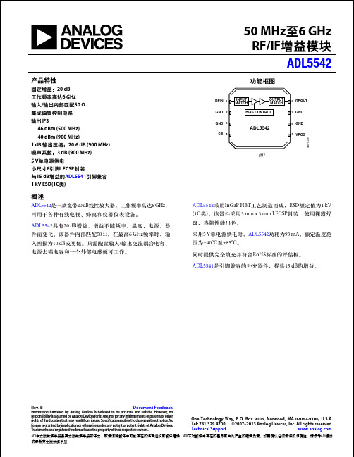
ADL5542 RF IF增益模块说明书
ADI 中文版数据手册是英文版数据手册的译文,敬请谅解翻译中可能存在的语言组织或翻译错误,ADI 不对翻译中存在的差异或由此产生的错误负责。
如需确认任何词语的准确性,请参考ADI 提供的最新英文版数据手册。
50 MHz 至6 GHz RF/IF 增益模块ADL5542Rev. BDocument Feedback Information furnished by Analog Devices is believed to be accurate and reliable. However , no responsibility is assumed by Analog Devices for its use, nor for any infringements of patents or other rights of third parties that may result from its use. Speci cations subject to change without notice. No license is granted by implication or otherwise under any patent or patent rights of Analog Devices. T rademarks and registered trademarks are the property of their respective owners.One Technology Way, P.O. Box 9106, Norwood, MA 02062-9106, U.S.A. Tel: 781.329.4700 ©2007–2013 Analog Devices, Inc. All rights reserved. Technical Support 功能框图2GND 7GND1RFIN 8RFOUT3GND 6GND4CB 5VPOSINPUT MATCHOUTPUT MATCHBIAS CONTROL ADL554206879-001图1.产品特性固定增益:20 dB 工作频率高达6 GHz 输入/输出内部匹配50 Ω集成偏置控制电路输出IP3 46 dBm (500 MHz)40 dBm (900 MHz)1 dB 输出压缩:20.6 dB (900 MHz)噪声系数:3 dB (900 MHz)5 V 单电源供电小尺寸8引脚LFCSP 封装与15 dB 增益的ADL5541引脚兼容1 kV ESD(1C 类)概述ADL5542是一款宽带20 dB 线性放大器,工作频率高达6 GHz ,可用于各种有线电视、蜂窝和仪器仪表设备。
AK5385BVFP-E2;AK5385BVSP-E2;中文规格书,Datasheet资料
MS0406-E-00 -2-
/
2005/08
ASAHI KASEI
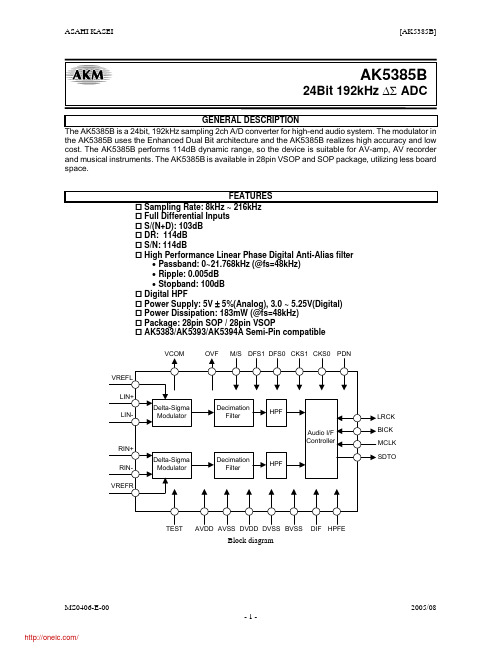
Compatibility with AK5383/AK5394A
Pin 1 Pin 2 Pin 3 Pin 6 Pin 9 Pin 11 Pin 12 Pin 16 Pin 18 Pin 20 Pin 26 Pin 27 Pin 28 fs MCLK at 48kHz MCLK at 96kHz MCLK at 192kHz DR, S/N Input Voltage Offset Calibration
• Passband: 0~21.768kHz (@fs=48kHz)
• Ripple: 0.005dB
• Stopband: 100dB Digital HPF Power Supply: 5V ± 5%(Analog), 3.0 ~ 5.25V(Digital) Power Dissipation: 183mW (@fs=48kHz) Package: 28pin SOP / 28pin VSOP AK5383/AK5393/AK5394A Semi-Pin compatible
Pin Layout
VREFL AVSS VCOM LIN+ LINCKS0 DVDD DVSS OVF PDN DIF M/S LRCK BICK
[AK5385B]
–10 ~ +70°C
28pin SOP (1.27mm pitch)
–40 ~ +85°C
28pin VSOP (0.65mm pitch)
FEATURES
Sampling Rate: 8kHz ~ 216kHz Full Differential Inputs S/(N+D): 103dB DR: 114dB S/N: 114dB High Performance Linear Phase Digital Anti-Alias filter
AD8532资料
a
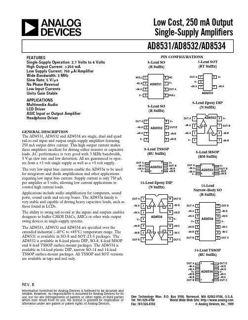
FEATURES Single-Supply Operation: 2.7 Volts to 6 Volts High Output Current: ؎ 250 mA Low Supply Current: 750 A/Amplifier Wide Bandwidth: 3 MHz Slew Rate: 5 V/ s No Phase Reversal Low Input Currents Unity Gain Stable APPLICATIONS Multimedia Audio LCD Driver ASIC Input or Output Amplifier Headphone Driver
8-Lead TSSOP (RU Suffix)
OUT A –IN A +IN A V– 1 8 V+ OUT B –IN B +IN B OUT A –IN A +IN A V–
8-Lead MSOP (RM Suffix)
1 8 V+ OUT B –IN B +IN B
AD8532
4 5
AD8532
Specifications subject to change without notice.
S
= +3.0 V, VCM = 1.5 V, TA = +25؇C unless otherwise noted)
Conditions Min Typ Max 25 30 50 60 25 30 3 Unit mV mV pA pA pA pA V dB V/mV µV/°C fA/ °C fA/ °C V V mV mV mA Ω dB mA mA V/µs µs MHz Degrees dB nV/√Hz nV/√Hz pA/√Hz
艾тон电子变频驱动器产品介绍说明书

V/Hz Energy Savings Percentage
Eaton - Active Energy Control Competitor 1 Competitor 2 Competitor 3
35
40
45
50
55
Frequency (Hz)
• Active Energy Control - minimizes energy losses in your motor by dynamically adjusting V/Hz curve to optimize efficiency
• Compare Functionality • PC Control Online Operate
Mode
© 2013 Eaton Corporation. All rights reserved.
13
Energy Saving Functionality
Percentage
10.0% 8.0% 6.0% 4.0% 2.0% 0.0% -2.0% 30 -4.0%
• Easy to Use PC Based Drive Software Configuration Tool
• Provides Parameter Description, Min, Max, and Default Values
• Monitoring and Data Logging Capabilities
© 2013 Eaton Corporation. All rights reserved.
Electrical Wholesalers
End Users Maintenance, Repair, and Operations (MRO) Opportunities
ADL5387中文资料
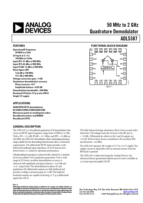
50 MHz to 2 GHzQuadrature DemodulatorADL5387 Rev. 0Information furnished by Analog Devices is believed to be accurate and reliable. However, noresponsibility is assumed by Analog Devices for its use, nor for any infringements of patents or other rights of third parties that may result from its use. Specifications subject to change without notice. No license is granted by implication or otherwise under any patent or patent rights of Analog Devices. T rademarks and registered trademarks are the property of their respective owners. One Technology Way, P.O. Box 9106, Norwood, MA 02062-9106, U.S.A. Tel: 781.329.4700 Fax: 781.461.3113 ©2007 Analog Devices, Inc. All rights reserved.FEATURESOperating RF frequency50 MHz to 2 GHzLO input at 2 × f LO100 MHz to 4 GHzInput IP3: 31 dBm @ 900 MHzInput IP2: 62 dBm @ 900 MHzInput P1dB: 13 dBm @ 900 MHzNoise figure (NF)12.0 dB @ 140 MHz14.7 dB @ 900 MHzVoltage conversion gain > 4 dB Quadrature demodulation accuracy Phase accuracy ~0.4°Amplitude balance ~0.05 dB Demodulation bandwidth ~240 MHz Baseband I/Q drive 2 V p-p into 200 Ω Single 5 V supply APPLICATIONSQAM/QPSK RF/IF demodulatorsW-CDMA/CDMA/CDMA2000/GSM Microwave point-to-(multi)point radios Broadband wireless and WiMAX Broadband CATVs FUNCTIONAL BLOCK DIAGRAM6764-1Figure 1.GENERAL DESCRIPTIONThe ADL5387 is a broadband quadrature I/Q demodulator that covers an RF/IF input frequency range from 50 MHz to 2 GHz. With a NF = 13.2 dB, IP1dB = 12.7 dBm, and IIP3 = 32 dBm @ 450 MHz, the ADL5387 demodulator offers outstanding dynamic range suitable for the demanding infrastructure direct-conversion requirements. The differential RF/IF inputs provide a well-behaved broadband input impedance of 50 Ω and are best driven from a 1:1 balun for optimum performance. Ultrabroadband operation is achieved with a divide-by-2 method for local oscillator (LO) quadrature generation. Over a wide range of LO levels, excellent demodulation accuracy is achieved with amplitude and phase balances ~0.05 dB and~0.4°, respectively. The demodulated in-phase (I) and quadrature (Q) differential outputs are fully buffered and provide a voltage conversion gain of >4 dB. The buffered baseband outputs are capable of driving a 2 V p-p differential signal into 200 Ω. The fully balanced design minimizes effects from second-order distortion. The leakage from the LO port to the RF port is<−70 dBc. Differential dc-offsets at the I and Q outputs are<10 mV. Both of these factors contribute to the excellent IIP2 specifications > 60 dBm.The ADL5387 operates off a single 4.75 V to 5.25 V supply. The supply current is adjustable with an external resistor from the BIAS pin to ground.The ADL5387 is fabricated using the Analog Devices, Inc. advanced silicon-germanium bipolar process and is available in a 24-lead exposed paddle LFCSP.ADL5387Rev. 0 | Page 2 of 28TABLE OF CONTENTSFeatures..............................................................................................1 Applications.......................................................................................1 Functional Block Diagram..............................................................1 General Description.........................................................................1 Revision History...............................................................................2 Specifications.....................................................................................3 Absolute Maximum Ratings............................................................5 ESD Caution..................................................................................5 Pin Configuration and Function Descriptions.............................6 Typical Performance Characteristics.............................................7 Distributions for f RF = 140 MHz...............................................10 Distributions for f RF = 450 MHz...............................................11 Distributions for f RF = 900 MHz...............................................12 Distributions for f RF = 1900 MHz.............................................13 Circuit Description.........................................................................14 LO Interface.................................................................................14 V-to-I Converter.........................................................................14 Mixers..........................................................................................14 Emitter Follower Buffers...........................................................14 Bias Circuit..................................................................................14 Applications.....................................................................................15 Basic Connections......................................................................15 Power Supply...............................................................................15 Local Oscillator (LO) Input......................................................15 RF Input.......................................................................................16 Baseband Outputs......................................................................16 Error Vector Magnitude (EVM) Performance.......................17 Low IF Image Rejection.............................................................18 Example Baseband Interface.....................................................18 Characterization Setups.................................................................21 Evaluation Board............................................................................23 Outline Dimensions.......................................................................26 Ordering Guide.. (26)REVISION HISTORY10/07—Revision 0: Initial VersionADL5387Rev. 0 | Page 3 of 28SPECIFICATIONSV S = 5 V , T A = 25°C, f RF = 900 MHz, f IF = 4.5 MHz, P LO = 0 dBm, BIAS pin open, Z O = 50 Ω, unless otherwise noted, baseband outputs differentially loaded with 450 Ω. Table 1.Parameter Condition Min Typ Max Unit OPERATING CONDITIONS LO Frequency Range External input = 2xLO frequency 0.1 4 GHz RF Frequency Range 0.05 2 GHz LO INPUT LOIP , LOIN Input Return LossAC-coupled into LOIP with LOIN bypassed,measured at 2 GHz−10 dB LO Input Level −6 0+6 dBm I/Q BASEBAND OUTPUTS QHI, QLO, IHI, ILOVoltage Conversion Gain 450 Ω differential load on I and Q outputs(@ 900 MHz)4.3 dB 200 Ω differential load on I and Q outputs(@ 900 MHz)3.2dBDemodulation Bandwidth 1 V p-p signal 3 dB bandwidth 240 MHz Quadrature Phase Error @ 900 MHz 0.4 Degrees I/Q Amplitude Imbalance 0.1 dB Output DC Offset (Differential) 0 dBm LO input ±5 mV Output Common-Mode VPOS − 2.8 V 0.1 dB Gain Flatness 40 MHz Output Swing Differential 200 Ω load 2 V p-p Peak Output Current Each pin 12 mA POWER SUPPLIES VPA, VPL, VPB, VPXVoltage 4.75 5.25 V Current BIAS pin open 180 mA RBIAS = 4 kΩ 157 mA DYNAMIC PERFORMANCE @ RF = 140 MHz RFIP , RFIN Conversion Gain 4.7 dB Input P1dB (IP1dB) 13 dBm Second-Order Input Intercept (IIP2) −5 dBm each input tone 67 dBm Third-Order Input Intercept (IIP3) −5 dBm each input tone 31 dBmLO to RF RFIN, RFIP terminated in 50 Ω, 1xLOappearing at the RF port−100 dBm RF to LO LOIN, LOIP terminated in 50 Ω −95 dBc I/Q Magnitude Imbalance 0.05 dB I/Q Phase Imbalance 0.2Degrees LO to I/Q RFIN, RFIP terminated in 50 Ω, 1xLOappearing at the BB port−39 dBm Noise Figure 12.0 dB Noise Figure under Blocking Conditions With a −5 dBm interferer 5 MHz away14.4dBADL5387Rev. 0 | Page 4 of 28Parameter Condition Min Typ Max Unit DYNAMIC PERFORMANCE @ RF = 450 MHz Conversion Gain 4.4 dB Input P1dB (IP1dB) 12.7 dBm Second-Order Input Intercept (IIP2) −5 dBm each input tone 69.2 dBm Third-Order Input Intercept (IIP3) −5 dBm each input tone 32.8 dBm LO to RF RFIN, RFIP terminated in 50 Ω, 1xLOappearing at the RF port−87 dBm RF to LO LOIN, LOIP terminated in 50 Ω −90 dBc I/Q Magnitude Imbalance 0.05 dB I/Q Phase Imbalance 0.6 Degrees LO to I/Q RFIN, RFIP terminated in 50 Ω, 1xLOappearing at the BB port−38 dBm Noise Figure 13.2 dB DYNAMIC PERFORMANCE @ RF = 900 MHz Conversion Gain 4.3 dB Input P1dB (IP1dB) 12.8 dBm Second-Order Input Intercept (IIP2) −5 dBm each input tone 61.7 dBm Third-Order Input Intercept (IIP3) −5 dBm each input tone 31.2 dBm LO to RF RFIN, RFIP terminated in 50 Ω, 1xLOappearing at the RF port−79 dBm RF to LO LOIN, LOIP terminated in 50 Ω −88 dBc I/Q Magnitude Imbalance 0.05 dB I/Q Phase Imbalance 0.2 Degrees LO to I/Q RFIN, RFIP terminated in 50 Ω,1XLO appearing at the BB port−41 dBm Noise Figure 14.7 dB Noise Figure under Blocking Conditions With a −5 dBm interferer 5 MHz away 15.8 dB DYNAMIC PERFORMANCE @ RF = 1900 MHzConversion Gain 3.8 dB Input P1dB (IP1dB)12.8 dBm Second-Order Input Intercept (IIP2) −5 dBm each input tone 59.8 dBm Third-Order Input Intercept (IIP3) −5 dBm each input tone27.4dBmLO to RFRFIN, RFIP terminated in 50 Ω, 1xLO appearing at the RF port−75 dBm RF to LOLOIN, LOIP terminated in 50 Ω −70 dBc I/Q Magnitude Imbalance 0.05 dB I/Q Phase Imbalance0.3Degrees LO to I/QRFIN, RFIP terminated in 50 Ω, 1xLO appearing at the BB port −43 dBm Noise Figure16.5 dB Noise Figure under Blocking ConditionsWith a −5 dBm interferer 5 MHz away18.7dBADL5387Rev. 0 | Page 5 of 28ABSOLUTE MAXIMUM RATINGSTable 2.Parameter Rating Supply Voltage VPOS1, VPOS2, VPOS3 5.5 V LO Input Power 13 dBm (re: 50 Ω) RF/IF Input Power 15 dBm (re: 50 Ω) Internal Maximum Power Dissipation 1100 mW θJA 54°C/WMaximum Junction Temperature 150°COperating Temperature Range −40°C to +85°CStorage Temperature Range −65°C to +125°CStresses above those listed under Absolute Maximum Ratingsmay cause permanent damage to the device. This is a stress rating only; functional operation of the device at these or any other conditions above those indicated in the operationalsection of this specification is not implied. Exposure to absolute maximum rating conditions for extended periods may affect device reliability. ESD CAUTIONADL5387Rev. 0 | Page 6 of 28PIN CONFIGURATION AND FUNCTION DESCRIPTIONS124CMRF CMRF RFIP ADL5387TOP VIEW(Not to Scale)RFIN CMRF VPX CML VPA COM BIASVPL VPL VPL VPB VPB QHI QLO IHI ILO LOIP LOIN CML CML COM232221201978910111223456181716151********-002Figure 2. Pin ConfigurationTable 3. Pin Function DescriptionsPin No. MnemonicDescription1, 4 to 6,17 to 19VPA, VPL, VPB, VPX Supply. Positive supply for LO, IF, biasing and baseband sections, respectively. These pins should be decoupled to board ground using appropriate sized capacitors. 2, 7, 10 to 12, 20, 23, 24COM, CML, CMRF Ground. Connect to a low impedance ground plane.3 BIAS Bias Control. A resistor can be connected between BIAS and COM to reduce the mixer core current. The default setting for this pin is open.8, 9LOIP , LOINLocal Oscillator. External LO input is at 2xLO frequency. A single-ended LO at 0 dBm can be applied through a 1000 pF capacitor to LOIP . LOIN should be ac-grounded, also using a 1000 pF. These inputs can also be driven differentially through a balun (recommended balun is M/A-COM ETC1-1-13). 13 to 16 ILO, IHI, QLO, QHII-Channel and Q-Channel Mixer Baseband Outputs. These outputs have a 50 Ω differential output impedance (25 Ω per pin). The bias level on these pins is equal to VPOS − 2.8 V. Each output pair can swing 2 V p-p (differential) into a load of 200 Ω. Output 3 dB bandwidth is 240 MHz.21, 22 RFIN, RFIPRF Input. A single-ended 50 Ω signal can be applied to the RF inputs through a 1:1 balun (recommended balun is M/A-COM ETC1-1-13). Ground-referenced inductors must also be connected to RFIP and RFIN (recommended values = 120 nH).EPExposed Paddle. Connect to a low impedance ground planeADL5387Rev. 0 | Page 7 of 28TYPICAL PERFORMANCE CHARACTERISTICSV S = 5 V , T A = 25°C, LO drive level = 0 dBm, R BIAS = open, unless otherwise noted.20151050200400600800100012001400160018002000G A I N (d B ), I P 1d B (d B m )RF FREQUENCY (MHz)06764-003Figure 3. Conversion Gain and Input 1 dB Compression Point (IP1dB) vs.RF Frequency80705030604020100200400600800100012001400160018002000I I P 2, I I P 3 (d B m )RF FREQUENCY (MHz)06764-004Figure 4. Input Third-Order Intercept (IIP3) andInput Second-Order Intercept Point (IIP2) vs. RF Frequency2.01.51.00.50–0.5–1.0–1.5–2.00200400600800100012001400160018002000M A G N I T U D E E R R O R (d B )RF FREQUENCY (MHz)06764-005Figure 5. I/Q Gain Mismatch vs. RF Frequency5–30–25–20–15–10–501100010010B B R E S P O N S E (d B )BB FREQUENCY (MHz)06764-006Figure 6. Normalized I/Q Baseband Frequency Response1917151311970200400600800100012001400160018002000N O I S E F I G U R E (d B )RF FREQUENCY (MHz)06764-007Figure 7. Noise Figure vs. RF Frequency43210–1–2–3–40200400600800100012001400160018002000Q U A D R A T U R E P H A S E E R R O R (D e g r e e s )RF FREQUENCY (MHz)06764-008Figure 8. I/Q Quadrature Phase Error vs. RF FrequencyADL5387Rev. 0 | Page 8 of 2820151050–6–5–4–3–2–10123456G A I N (d B ), I N P U T P 1d B (d B m ), N O I S E F I G U R E (d B )8065503520I N P U T I P 2, I N P U T I P 3 (d B m )LO LEVEL (dBm)06764-009Figure 9. Conversion Gain, Noise Figure, IIP3, IIP2, and IP1dB vs.LO Level, f RF = 140 MHz3228242016128110100I I P 3 (d B m ) A N D N O I S E F I G U R E (d B )S U P P L Y C U R R E N T (m A )R BIAS (k Ω)06764-010Figure 10. Noise Figure, IIP3, and Supply Current vs. R BIAS , f RF= 140 MHz2520151050–3050–5–10–15–20–25N O I S E F I G U R E (d B )RF BLOCKER INPUT POWER (dBm)06764-011Figure 11. Noise Figure vs. Input Blocker Level, f RF = 900 MHz(RF Blocker 5 MHz Offset)20151050–6–5–4–3–2–1123456G A I N (d B ), I N P U T P 1d B (d B m ), N O I S E F I G U R E(d B )I N P U T I P 2, I N P U T I P 3 (d B m )LO LEVEL (dBm)06764-012Figure 12. Conversion Gain, Noise Figure, IIP3, IIP2, and IP1dB vs.LO Level, f RF = 900 MHz3228242016128110I I P 3 (d B m ) A N D N O I S E F I G U R E (d B )R BIAS (k Ω)10006764-013Figure 13. IIP3 and Noise Figure vs. R BIAS , f RF = 900 MHz80706050403020100110G A I N (d B ), IP 1d B , I I P 2, I A N D Q C H A N N E L S (d B m )R BIAS (k Ω)10006764-014Figure 14. Conversion Gain, IP1dB, IIP2 I Channel, and IIP2 Q Channel vs. R BIASADL5387Rev. 0 | Page 9 of 28353025201510505045403530252015105I P 1d B , I I P 3 (d B m )IN P U T I P 2, I A N D Q C H A N N E L S (d B m )BB FREQUENCY (MHz)–20–30–40–50–60–70–80–90–1000200018001600140012001000800600400200L O L E A K A G E (d B m )INTERNAL 1xLO FREQUENCY (MHz)06764-01506764-018Figure 15. IIIP3, IIP2, IP1dB vs. Baseband Frequency0–10–20–30–40–50–60–70–800200018001600140012001000800600400200F E E D T H R O U G H (d B m )INTERNAL 1xLO FREQUENCY (MHz)06764-016Figure 16. LO-to-BB Feedthrough vs. 1xLO Frequency (Internal LO Frequency)–25–20–15–10–50200018001600140012001000800600400200R E T U R N L O S S (d B )RF FREQUENCY (MHz)06764-017Figure 17. RF Port Return Loss vs. RF Frequency, Measured onCharacterization Board through ETC1-1-13 Balun with 120 nH Bias InductorsFigure 18. LO-to-RF Leakage vs. Internal 1xLO Frequency–20–40–60–80–100–1200200018001600140012001000800600400200L E A K A G E (d B c )RF FREQUENCY (MHz)06764-019Figure 19. RF-to-LO Leakage vs. RF Frequency–30–25–20–15–10–504000350030002500200015001000500R E T U R N L O S S (d B )FREQUENCY (MHz)06764-020Figure 20. Single-Ended LO Port Return Loss vs. LO Frequency, LOIN AC-Coupled to GroundADL5387Rev. 0 | Page 10 of 28DISTRIBUTIONS FOR f RF = 140 MHz100020406080283330293231P E R C E N T A G E (%)INPUT IP3 (dBm)06764-021Figure 21. IIP3 Distributions100020406080101512111413P E R C E N T A G E (%)INPUT P1dB (dBm)06764-022Figure 22. IP1dB Distributions100020406080–0.20.2–0.10.1P E R C E N T A G E (%)I/Q GAIN MISMATCH (dB)06764-023Figure 23. I/Q Gain Mismatch Distributions10002040608060756570P E R C E N T A G E (%)INPUT IP2 (dBm)06764-024Figure 24. IIP2 Distributions for I Channel and Q Channel10002040608010.513.513.012.512.011.511.0P E R C E N T A G E(%)NOISE FIGURE (dB)06764-025Figure 25. Noise Figure Distributions100020406080–1.01.00.50–0.5P E R C E N T A G E(%)QUADRATURE PHASE ERROR (Degrees)06764-026Figure 26. I/Q Quadrature Error DistributionsADL5387DISTRIBUTIONS FOR f RF = 450 MHz100020406080303534333231P E R C E N T A G E (%)INPUT IP3 (dBm)06764-027Figure 27. IIP3 Distributions100020406080101514131211P E R C E N T A G E (%)INPUT P1dB (dBm)06764-028Figure 28. IP1dB Distributions100020406080–0.20.20.10–0.1P E R C E N T A G E (%)I/Q GAIN MISMATCH (dB)06764-029Figure 29. I/Q Gain Mismatch Distributions10002040608060756570P E R C E N T A G E (%)INPUT IP2 (dBm)06764-030Figure 30. IIP2 Distributions for I Channel and Q Channel10002040608012.015.014.514.013.513.012.5P E R C E N TA G E (%)NOISE FIGURE (dB)06764-031Figure 31. Noise Figure Distributions100020406080–1.0–0.500.5 1.0P E R C E N T A G E(%)QUADRATURE PHASE ERROR (Degrees)06764-032Figure 32. I/Q Quadrature Error DistributionsADL5387DISTRIBUTIONS FOR f RF = 900 MHz100020406080303133323435P E R C E N T A G E (%)INPUT IP3 (dBm)06764-033Figure 33. IIP3 Distributions100020406080101113121415P E R C E N T A G E (%)INPUT P1dB (dBm)06764-034Figure 34. IP1dB Distributions100020406080–0.2–0.100.10.2P E R C E N T A G E (%)I/Q GAIN MISMATCH (dB)06764-035Figure 35. I/Q Gain Mismatch Distributions1000204060805575656070P E R C E N T A G E (%)INPUT IP2 (dBm)06764-036Figure 36. IIP2 Distributions for I Channel and Q Channel10002040608013.013.514.014.515.015.516.0P E R C E N T AG E (%)NOISE FIGURE (dB)06764-037Figure 37. Noise Figure Distributions100020406080–1.01.00.50–0.5P E R C E N TA G E (%)QUADRATURE PHASE ERROR (Degrees)06764-038Figure 38. I/Q Quadrature Error DistributionsADL5387DISTRIBUTIONS FOR f RF = 1900 MHz100020406080263129302827P E R C E N T A G E (%)INPUT IP3 (dBm)06764-039Figure 39. IIP3 Distributions100020406080101513141211P E R C E N T A G E (%)INPUT P1dB (dBm)06764-040Figure 40. IP1dB Distributions100020406080–0.20.20.10–0.1P E R C E N T A G E (%)I/Q GAIN MISMATCH (dB)06764-041Figure 41. I/Q Gain Mismatch Distributions100020406080526866646260585654P E R C E N T A G E (%)INPUT IP2 (dBm)06764-042Figure 42. IIP2 Distributions for I Channel and Q Channel10002040608015.018.017.517.016.516.015.5P E R C E N T AG E (%)NOISE FIGURE (dB)06764-043Figure 43. Noise Figure Distributions100020406080–1.01.00.50–0.5P E R C E N T AG E (%)QUADRATURE PHASE ERROR (Degrees)06764-044Figure 44. I/Q Quadrature Error DistributionsADL5387CIRCUIT DESCRIPTIONThe ADL5387 can be divided into five sections: the local oscillator (LO) interface, the RF voltage-to-current (V-to-I) converter, the mixers, the differential emitter follower outputs, and the bias circuit. A detailed block diagram of the device is shown in Figure 45.RFIP RFIN06764-045Figure 45. Block DiagramThe LO interface generates two LO signals at 90° of phase difference to drive two mixers in quadrature. RF signals are converted into currents by the V-to-I converters that feed into the two mixers. The differential I and Q outputs of the mixers are buffered via emitter followers. Reference currents to each section are generated by the bias circuit. A detailed description of each section follows.LO INTERFACEThe LO interface consists of a buffer amplifier followed by a frequency divider that generate two carriers at half the input frequency and in quadrature with each other. Each carrier is then amplified and amplitude-limited to drive the double-balanced mixers. V-TO-I CONVERTERThe differential RF input signal is applied to a resistivelydegenerated common base stage, which converts the differential input voltage to output currents. The output currents thenmodulate the two half-frequency LO carriers in the mixer stage.MIXERSThe ADL5387 has two double-balanced mixers: one for the in-phase channel (I channel) and one for the quadrature channel (Q channel). These mixers are based on the Gilbert cell design of four cross-connected transistors. The output currents from the two mixers are summed together in the resistive loads that then feed into the subsequent emitter follower buffers.EMITTER FOLLOWER BUFFERSThe output emitter followers drive the differential I and Q signals off-chip. The output impedance is set by on-chip 25 Ω series resistors that yield a 50 Ω differential output impedance for each baseband port. The fixed output impedance forms a voltage divider with the load impedance that reduces the effective gain. For example, a 500 Ω differential load has 1 dB lower effective gain than a high (10 kΩ) differential load impedance.BIAS CIRCUITA band gap reference circuit generates the proportional-to-absolute temperature (PTAT) as well as temperature-independent reference currents used by different sections. The mixer current can be reduced via an external resistor between the BIAS pin and ground. When the BIAS pin is open, the mixer runs at maximum current and hence the greatest dynamic range. The mixer current can be reduced by placing a resistance to ground; therefore, reducing overall power consumption, noise figure, and IIP3. The effect on each of these parameters is shown in Figure 10, Figure 13, and Figure 14.ADL5387APPLICATIONS INFORMATIONBASIC CONNECTIONSFigure 47 shows the basic connections schematic for the ADL5387.POWER SUPPLYThe nominal voltage supply for the ADL5387 is 5 V and is applied to the VPA, VPB, VPL, and VPX pins. Ground should be connected to the COM, CML, and CMRF pins. Each of the supply pins should be decoupled using two capacitors; recommended capacitor values are 100 pF and 0.1 μF .LOCAL OSCILLATOR (LO) INPUTThe LO port is driven in a single-ended manner. The LO signal must be ac-coupled via a 1000 pF capacitor directly into LOIP , and LOIN is ac-coupled to ground also using a 1000 pF capacitor. The LO port is designed for a broadband 50 Ω match andtherefore exhibits excellent return loss from 100 MHz to 4 GHz. The LO return loss can be seen in Figure 20. Figure 46 shows the LO input configuration.06764-047Figure 46. Single-Ended LO DriveThe recommended LO drive level is between −6 dBm and+6 dBm. The LO frequency at the input to the device should be twice that of the desired LO frequency at the mixer core. The applied LO frequency range is between 100 MHz and 4 GHz.0.1µFV POSV POS06764-046ADL5387RF INPUTThe RF inputs have a differential input impedance ofapproximately 50 Ω. For optimum performance, the RF port should be driven differentially through a balun. The recommended balun is M/A-COM ETC1-1-13. The RF inputs to the device should be ac-coupled with 1000 pF capacitors. Ground-referenced choke inductors must also be connected to RFIP and RFIN (recommended value = 120 nH, Coilcraft 0402CS-R12XJL) for appropriate biasing. Several important aspects must be taken into account when selecting an appropriate choke inductor for this application. First, the inductor must be able to handle the approximately 40 mA of standing dc current being delivered from each of the RF input pins (RFIP , RFIN). (The suggested 0402 inductor has a 50 mA current rating). The purpose of the choke inductors is to provide a very low resistance dc path to ground and high ac impedance at the RF frequency so as not to affect the RF input impedance. A choke inductor that has a self-resonant frequency greater than the RF input frequency ensures that the choke is still looking inductive and therefore has a more predictable ac impedance (jωL) at the RF frequency. Figure 48 shows the RF input configuration.06764-048Figure 48. RF InputThe differential RF port return loss has been characterized as shown in Figure 49.–10–12–14–16–18–20–22–24–26–2800.20.40.60.8 1.0 1.2 1.4 1.6 1.8 2.0S (1, 1) (d B )FREQUENCY (GHz)06764-049Figure 49. Differential RF Port Return LossBASEBAND OUTPUTSThe baseband outputs QHI, QLO, IHI, and ILO are fixed impedance ports. Each baseband pair has a 50 Ω differential output impedance. The outputs can be presented with differential loads as low as 200 Ω (with some degradation in linearity and gain) or high impedance differential loads (500 Ω or greater impedance yields the same excellent linearity) that is typical of an ADC. The TCM9-1 9:1 balun converts the differential IF output to single-ended. When loaded with 50 Ω, this balun presents a 450 Ω load to the device. The typical maximum linear voltage swing for these outputs is 2 V p-p differential. The bias level on these pins is equal to VPOS − 2.8 V . The output 3 dB bandwidth is 240 MHz. Figure 50 shows the baseband output configuration.QHIQLOIHIILOQHI QLO IHI ILO 06764-050Figure 50. Baseband Output ConfigurationADL5387ERROR VECTOR MAGNITUDE (EVM) PERFORMANCEEVM is a measure used to quantify the performance of a digital radio transmitter or receiver. A signal received by a receiver would have all constellation points at the ideal locations; however, various imperfections in the implementation (such as carrier leakage, phase noise, and quadrature error) cause the actual constellation points to deviate from the ideal locations. The ADL5387 shows excellent EVM performance for various modulation schemes. Figure 51 shows typical EVM performance over input power range for a point-to-point application with 16 QAM modulation schemes and zero-IF baseband. The differential dc offsets on the ADL5387 are in the order of a few mV . However, ac coupling the baseband outputs with 10 μF capacitors helps to eliminate dc offsets and enhances EVM performance. With a 10 MHz BW signal, 10 μF ac coupling capacitors with the 500 Ω differential load results in a high-pass corner frequency of ~64 Hz which absorbs an insignificant amount of modulated signal energy from the baseband signal. By using ac coupling capacitors at the baseband outputs, the dc offset effects, which can limit dynamic range at low input power levels, can be eliminated.0–50–45–40–35–30–25–20–15–10–5–7010–10–20–30–40–50–60E V M (d B )INPUT POWER (dBm)06764-051Figure 51. RF = 140 MHz, IF = 0 Hz, EVM vs. Input Power for a 16 QAM10 Msym/s Signal (AC-Coupled Baseband Outputs)Figure 52 shows the EVM performance of the ADL5387 when ac-coupled, with an IEEE 802.16e WiMAX signal.0–50–45–40–35–30–25–20–15–10–5–502010–10–20–30–40E V M (d B )INPUT POWER (dBm)06764-052Figure 52. RF = 750MHz MHz, IF = 0 Hz, EVM vs. Input Power for a 16 QAM 10 MHz Bandwidth Mobile WiMAX Signal (AC-Coupled Baseband Outputs)Figure 53 exhibits the zero IF EVM performance of a WCDMA signal over a wide RF input power range.0–45–40–35–30–25–20–15–10–5–70–60100–10–20–30–40–50E V M (d B)INPUT POWER (dBm)06764-053Figure 53. RF = 1950 MHz, IF = 0 Hz, EVM vs. Input Power for a WCDMA(AC-Coupled Baseband Outputs)。
CHI MEI PA-765B E56070 元件说明书

•Component •元件UL file numberUL档案号Part number型号Remark备注Vendor供应商•FRONT CASE•前身E56070 PA-765B CHI MEI•TOP CASE•上身E56070 PA-765B CHI MEI•BOTTOM CASE•下身E56070 PA-765B CHI MEI•Batterycompartment•电池箱E207780 PC945(GG) QMFZ2 SABIC JAPAN L L C•Transformercover•火牛上盖E50075 LV2250V TEIJIN•TransformerHousing 火牛下盖E50075 LV2250V TEIJIN•Aux foam pad•Aux盖E257267 E50A-60 ZHI JIN•Side plate•侧盖E56070 PA-765B CHI MEI•Battery BayRubber Cover•电池箱盖E257267 E50A-60 ZHI JIN•batterydoors•电池盖E56070 PA-765B CHI MEI•AAA batterycover•3A 电池门E56070 PA-765B CHI MEI•Light guide•导光片E54705 CL PMMA SUMIPEX•Frontcontrolpanel 显示压件E248280 PC+ABS Jacobson•Strainrelief•线卡E107293 6P-4 晋煜•Power cord •电源线E137516 SJTW ZJCZ 利源電業製品廠有限公司LEE YUEN ELECTRICAL MFY LTD. E143681 LY-13B ELBZ7•Lead wire •引线E244721 UL 1007 20AWGL=330mmAVLV2 惠州市远达电业五金制品有限公司HUI ZHOU YUEN DA ELECTRONIC & HARDWARECO.,LTDE329541 UL 1007 18AWGVH3.96-H-2PVH3.96-TL=186mmZPFW2 深圳艾格科技有限公司Shenzhen Aiger Technology Co.,LtdE330646 UL 1007#24 XH-TXH-4P L=140mmAVLV2 深圳市展旺连接器有限公司Shen Zhen Zhan Wang Linker CO.,LTDE330646 UL 1007#24 XH-TXH-2P L=260mmAVLV2E330646 UL 2547#28 PH-TPH-3P L=260mmAVLV2E330646 UL 2547#28 PH-TPH-3P L=220mmAVLV2E330646 UL 1185 22AWG XH-T XH-2P L=150mmAVLV2•Integralfuse •保险丝E340427 SFC0800A(800mA/250V FastActing Glass TubeFuse)JDYX 瑞卓电子(东莞)有限公司Dongguan Reomax Electronics Co., LTD•Fuse Holder •保险丝座E239034 H3(10A/250V)IZLT2 惠州市海牛電子有限公司HUIZHOU HINEW ELECTRIC APPLIANCE CO.,LTD.变压器材料清單/ MATERIAL LISTNO. MATERIAL DESCRIPTION Ul file MANUFACTURERS / SUPPLIERS1. 膠芯/Bobbin 最小0.71mm厚尼龍66 101(r9)一層minimum 0.71mm thick PA66101(r9) one layerUL:E41938 杜邦/E I Dupont De Nemours & Co Inc2 膠套/Shroud 最小0.50mm厚尼龍66 101(r9)一層minimum 0.50mm thick PA66101(r9) one layerUL:E41938 杜邦/E I Dupont De Nemours & Co Inc3 初級線圈PrimaryWinding 聚氨酯漆包線MW75C(130℃) 或Polyurethane Wire,MW75C(130℃)UL:E258125 河源天裕電子塑膠有限公司He Yuan Sky Wealth Electronic And PlasticCo Ltd.4 初級跨線絕緣Pri. windingcrossoverinsulation CT25聚脂膠紙/CT-25 Polyestertape厚度:0.05mm*2 層/Thickness:0.05mm*2 layersUL:E165111 靖江亞華壓敏黏膠有限公司Jingjiang Yahua Pressure Sensitive Glue COLTD5 溫度保險Thermal Fuse Type: A4-F130 Deg.C ( 250V/2A)UL:E140847 雅寶電子有限公司/Aupo Electronics Inc.6 初級引線Primary Leads UL-1672 AWG #22 VW-1 300V105Deg.CUL:E191230UL:E189674UL:E211048UL:E214859恒輝(香港)發展有限公司Ever Bright (Hongkong) development CompanyLimited.深圳东聚Shenzhen Dong Ju Wire & CableCo.,Ltd.琦富瑞Qifurui Electronics co阳泰氟电线电缆YANGTAI WIRE & CABLE CO LTD7 初級引線Primary Leads 聚氨酯漆包線MW75C(130℃) 或Polyurethane Wire,MW75C(130℃)or聚氨酯漆包線MW79C(155℃)Polyurethane Wire,MW79C(155℃)UL:E258125UL:E201757河源天裕電子塑膠有限公司He Yuan Sky Wealth Electronic And PlasticCo Ltd.太平洋電線電纜深圳公司Pacific ElectricWire&Cable(shenzhen)Co.,Ltd.8 次級引線SecondaryLeads UL-1015 AWG #20 VW-1 600V105Deg.CUL:E191230UL:E189674UL:E211048UL:E214859恒輝(香港)發展有限公司Ever Bright(Hongkong) development Company Limited.深圳东聚Shenzhen Dong Ju Wire & CableCo.,Ltd.琦富瑞Qifurui Electronics co阳泰氟电线电缆YANGTAI WIRE & CABLE CO LTD9 次級引線SecondaryLeads CT25聚脂膠紙/CT-25 Polyestertape厚度:0.05mm*3 層/UL:E165111 靖江亞華壓敏黏膠有限公司Jingjiang Yahua Pressure Sensitive Glue COLTD.Thickness:0.05mm*3 layers聚酯膠片型號:MYLAR EL21 0.25mm厚PET film Type:MYLAR EL21 0.25mmThickUL:E93687 杜邦帝人/ Dupont Teijin Films U S L P10 外層絕緣Outinsulation CT25聚脂膠紙/CT-25 Polyestertape厚度:0.05mm*3 層/Thickness:0.05mm*3 layers聚酯膠片型號:MYLAR EL21 0.25mm厚PET film Type:MYLAR EL21 0.25mmThickUL:E165111UL:E93687靖江亞華壓敏黏膠有限公司Jingjiang Yahua Pressure Sensitive Glue COLTD.杜邦帝人/ Dupont Teijin Films U S L P11 鐵芯片LaminationCore EI-57 硅鋼片(H18 黑) 片厚0.50,疊厚35.3+/-0.5mmEI-57 silicon steel sheet(H18black), thickness:0.50mm,depth thickness:35.3+/-0.5mmN/A 東莞東駿電器有限公司Dongguan Dongjun Electrical Appliances Co.,Ltd.12 安裝架/Bracket 冷軋板鍍鋅Cold rolled Steel with Zinc-coatedN/A 東莞駿豐五金製品廠Dongguan JunFeng MetalManufactory13 屏蔽殼/Endbell 冷軋板鍍鋅Cold rolled Steel with Zinc-coatedN/A 東莞駿豐五金製品廠Dongguan JunFeng MetalManufactory14 次級連接器Secondaryconnector Housing: JS-1121-02 & Terminal:JS-1121-THousing: A3963H-2P & Terminal:A3963-TPUL: E113875UL: E326732喬訊電子有限公司Chyao shiunn electronicIndustrial Ltd.長江連接器有限公司ChangJiang Connectors CoLtd15 浸漬/Impregnation Insulating Varnish/絕緣油Type: 8562/C, class FUL:E200154 恒昌化學塗料公司HANG CHEUNG PETROCHEMICALLTD。
- 1、下载文档前请自行甄别文档内容的完整性,平台不提供额外的编辑、内容补充、找答案等附加服务。
- 2、"仅部分预览"的文档,不可在线预览部分如存在完整性等问题,可反馈申请退款(可完整预览的文档不适用该条件!)。
- 3、如文档侵犯您的权益,请联系客服反馈,我们会尽快为您处理(人工客服工作时间:9:00-18:30)。
700 MHz to 2.7 GHzQuadrature DemodulatorADL5382 Rev. 0Information furnished by Analog Devices is believed to be accurate and reliable. However, noresponsibility is assumed by Analog Devices for its use, nor for any infringements of patents or other rights of third parties that may result from its use. Specifications subject to change without notice. No license is granted by implication or otherwise under any patent or patent rights of Analog Devices. T rademarks and registered trademarks are the property of their respective owners. One Technology Way, P.O. Box 9106, Norwood, MA 02062-9106, U.S.A. Tel: 781.329.4700 Fax: 781.461.3113 ©2008 Analog Devices, Inc. All rights reserved.FEATURESOperating RF and LO frequency: 700 MHz to 2.7 GHz Input IP333.5 dBm @ 900 MHz30.5 dBm @1900 MHzInput IP2: >70 dBm @ 900 MHzInput P1dB: 14.7 dBm @ 900 MHzNoise figure (NF)14.0 dB @ 900 MHz15.6 dB @ 1900 MHzVoltage conversion gain: ~4 dBQuadrature demodulation accuracyPhase accuracy: ~0.2°Amplitude balance: ~0.05 dBDemodulation bandwidth: ~370 MHzBaseband I/Q drive: 2 V p-p into 200 ΩSingle 5 V supplyAPPLICATIONSCellular W-CDMA/CDMA/CDMA2000/GSM Microwave point-to-(multi)point radios Broadband wireless and WiMAXFUNCTIONAL BLOCK DIAGRAMVPACOMBIASVPLVPLVPLVPBVPBQHIQLOIHIILO728-1Figure 1.GENERAL DESCRIPTIONThe ADL5382 is a broadband quadrature I-Q demodulator that covers an RF input frequency range from 700 MHz to 2.7 GHz. With a NF = 14 dB, IP1dB = 14.7 dBm, and IIP3 = 33.5 dBm at 900 MHz, the ADL5382 demodulator offers outstanding dynamic range suitable for the demanding infrastructure direct-conversion requirements. The differential RF inputs provide a well-behaved broadband input impedance of 50 Ω and are best driven from a 1:1 balun for optimum performance.Excellent demodulation accuracy is achieved with amplitude and phase balances ~0.05 dB and ~0.2°, respectively. The demodulated in-phase (I) and quadrature (Q) differential outputs are fully buffered and provide a voltage conversion gain of ~4 dB. The buffered baseband outputs are capable of driving a 2 V p-p differential signal into 200 Ω. The fully balanced design minimizes effects from second-order distortion. The leakage from the LO port to the RF port is<−65 dBc. Differential dc offsets at the I and Q outputs are typically <10 mV. Both of these factors contribute to the excellent IIP2 specifications which is >60 dBm.The ADL5382 operates off a single 4.75 V to 5.25 V supply. The supply current is adjustable with an external resistor from the BIAS pin to ground.The ADL5382 is fabricated using the Analog Devices, Inc., advanced Silicon-Germanium bipolar process and is available in a 24-lead exposed paddle LFCSP.ADL5382Rev. 0 | Page 2 of 28TABLE OF CONTENTSFeatures..............................................................................................1 Applications.......................................................................................1 Functional Block Diagram..............................................................1 General Description.........................................................................1 Revision History...............................................................................2 Specifications.....................................................................................3 Absolute Maximum Ratings............................................................5 ESD Caution..................................................................................5 Pin Configuration and Function Descriptions.............................6 Typical Performance Characteristics.............................................7 Distributions for f RF = 900 MHz...............................................10 Distributions for f RF = 1900 MHz.............................................11 Distributions for f RF = 2700 MHz.............................................12 Circuit Description.........................................................................13 LO Interface.................................................................................13 V-to-I Converter.........................................................................13 Mixers..........................................................................................13 Emitter Follower Buffers...........................................................13 Bias Circuit..................................................................................13 Applications Information..............................................................14 Basic Connections......................................................................14 Power Supply...............................................................................14 Local Oscillator (LO) Input......................................................14 RF Input.......................................................................................15 Baseband Outputs......................................................................15 Error V ector Magnitude (EVM) Performance...........................16 Low IF Image Rejection.............................................................17 Example Baseband Interface.....................................................17 Characterization Setups.................................................................21 Evaluation Board............................................................................23 Outline Dimensions.......................................................................27 Ordering Guide.. (27)REVISION HISTORY3/08—Revision 0: Initial VersionADL5382Rev. 0 | Page 3 of 28SPECIFICATIONSV S = 5 V , T A = 25°C, f LO = 900 MHz, f IF = 4.5 MHz, P LO = 0 dBm, BIAS pin open, Z O = 50 Ω, unless otherwise noted. Baseband outputs differentially loaded with 450 Ω. Loss of the balun used to drive the RF port was de-embedded from these measurements. Table 1.Parameter Condition Min Typ Max UnitOPERATING CONDITIONS LO and RF Frequency Range 0.7 2.7 GHz LO INPUT LOIP , LOIN Input Return Loss LO driven differentially through a balun at 900 MHz −11 dB LO Input Level −6 0 +6 dBm I/Q BASEBAND OUTPUTS QHI, QLO, IHI, ILO Voltage Conversion Gain 450 Ω differential load on I and Q outputs at 900 MHz 3.9 dB 200 Ω differential load on I and Q outputs at 900 MHz 3.0 dB Demodulation Bandwidth 1 V p-p signal, 3 dB bandwidth 370 MHz Quadrature Phase Error At 900 MHz 0.2 Degrees I/Q Amplitude Imbalance 0.05 dB Output DC Offset (Differential) 0 dBm LO input at 900 MHz ±5 mV Output Common Mode VPOS − 2.8 V 0.1 dB Gain Flatness 50 MHz Output Swing Differential 200 Ω load 2 V p-p Peak Output Current Each pin 12 mA POWER SUPPLIES VPA, VPL, VPB, VPXVoltage 4.75 5.25 V Current BIAS pin open 220 mA R BIAS = 4 kΩ 196 mA DYNAMIC PERFORMANCE at RF = 900 MHz Conversion Gain 3.9 dB Input P1dB 14.7 dBm Second-Order Input Intercept (IIP2) −5 dBm each input tone 73 dBm Third-Order Input Intercept (IIP3) −5 dBm each input tone 33.5 dBm LO to RF RFIN, RFIP terminated in 50 Ω −92 dBm RF to LO LOIN, LOIP terminated in 50 Ω −89 dBc IQ Magnitude Imbalance 0.05 dB IQ Phase Imbalance 0.2 Degrees LO to IQ RFIN, RFIP terminated in 50 Ω −43 dBm Noise Figure 14.0 dB Noise Figure under Blocking Conditions With a −5 dBm interferer 5 MHz away 19.9 dB DYNAMIC PERFORMANCE at RF = 1900 MHz Conversion Gain 3.9 dB Input P1dB 14.4 dBm Second-Order Input Intercept (IIP2) −5 dBm each input tone 65 dBm Third-Order Input Intercept (IIP3) −5 dBm each input tone 30.5 dBm LO to RF RFIN, RFIP terminated in 50 Ω −71 dBm RF to LO LOIN, LOIP terminated in 50 Ω −78 dBc IQ Magnitude Imbalance 0.05 dB IQ Phase Imbalance 0.2 Degrees LO to IQ RFIN, RFIP terminated in 50 Ω −41 dBm Noise Figure 15.6 dB Noise Figure under Blocking Conditions With a −5 dBm interferer 5 MHz away20.5 dBADL5382Rev. 0 | Page 4 of 28Parameter Condition Min Typ Max UnitDYNAMIC PERFORMANCE at RF = 2700 MHz RFIP , RFIN Conversion Gain 3.3 dB Input P1dB 14.5 dBm Second-Order Input Intercept (IIP2) −5 dBm each input tone 52 dBm Third-Order Input Intercept (IIP3) −5 dBm each input tone 28.3 dBm LO to RF RFIN, RFIP terminated in 50 Ω, 1xLO appearing at RF port −70 dBm RF to LO LOIN, LOIP terminated in 50 Ω −55 dBc IQ Magnitude Imbalance 0.16 dB IQ Phase Imbalance 0.1 Degrees LO to IQ RFIN, RFIP terminated in 50 Ω, 1xLO appearing at BB port −42 dBm Noise Figure 17.6 dBADL5382Rev. 0 | Page 5 of 28ABSOLUTE MAXIMUM RATINGSTable 2.Parameter RatingSupply Voltage (VPA, VPL, VPB, VPX) 5.5 VLO Input Power 13 dBm (re: 50 Ω)RF Input Power 15 dBm (re: 50 Ω)Internal Maximum Power Dissipation 1230 mWθJA54°C/W Maximum Junction Temperature150°COperating Temperature Range −40°C to +85°C Storage Temperature Range −65°C to +125°CStresses above those listed under Absolute Maximum Ratings may cause permanent damage to the device. This is a stress rating only; functional operation of the device at these or any other conditions above those indicated in the operational section of this specification is not implied. Exposure to absolute maximum rating conditions for extended periods may affect device reliability.ESD CAUTIONADL5382Rev. 0 | Page 6 of 28PIN CONFIGURATION AND FUNCTION DESCRIPTIONS124CMRF CMRF RFIP ADL5382TOP VIEW(Not to Scale)RFIN CMRF VPX CML VPA COM BIASVPL VPL VPL VPB VPB QHI QLO IHI ILO LOIP LOIN CML CML COM232221201978910111223456181716151********-002Figure 2. Pin ConfigurationTable 3. Pin Function DescriptionsPin No. MnemonicDescription1, 4 to 6,17 to 19VPA, VPL, VPB, VPX Supply. Positive supply for LO, IF, biasing, and baseband sections. These pins should be decoupled to the board ground using appropriate-sized capacitors. 2, 7, 10 to 12, 20, 23, 24COM, CML, CMRF Ground. Connect to a low impedance ground plane.3 BIAS Bias Control. A resistor (R BIAS ) can be connected between BIAS and COM to reduce the mixer core current. The default setting for this pin is open.8, 9 LOIP , LOIN Local Oscillator Input. Pins must be ac-coupled. A differential drive through a balun (recommended balun is the M/A-COM ETC1-1-13) is necessary to achieve optimal performance.13 to 16ILO, IHI, QLO, QHII Channel and Q Channel Mixer Baseband Outputs. These outputs have a 50 Ω differential output impedance (25 Ω per pin). The bias level on these pins is equal to VPOS − 2.8 V. Each output pair can swing 2 V p-p (differential) into a load of 200 Ω. Output 3 dB bandwidth is 370 MHz.21, 22 RFIN, RFIPRF Input. A single-ended 50 Ω signal can be applied to the RF inputs through a 1:1 balun (recommended balun is the M/A-COM ETC1-1-13). Ground-referenced inductors must also be connected to RFIP and RFIN (recommended values = 33 nH).EPExposed Paddle. Connect to a low impedance thermal and electrical ground plane.ADL5382Rev. 0 | Page 7 of 28TYPICAL PERFORMANCE CHARACTERISTICSV S = 5 V , T A = 25°C, LO drive level = 0 dBm, R BIAS = open, RF input balun loss is de-embedded, unless otherwise noted.07208-003RF FREQUENCY (MHz)G A I N (d B ), I P 1d B (d B m )Figure 3. Conversion Gain and Input IP1 dB Compression Point (IP1dB) vs.RF Frequency102030405060708070090011001300150017001900210023002500270007208-004RF FREQUENCY (MHz)I I P 3, I I P 2 (d B m )Figure 4. Input Third-Order Intercept (IIP3) andInput Second-Order Intercept Point (IIP2) vs. RF Frequency–2.0–1.5–1.00–0.50.51.01.52.070090011001300150017001900210023002500270007208-005RF FREQUENCY (MHz)G A I N M I S M A T C H (d B )Figure 5. IQ Gain Mismatch vs. RF Frequency–8–7–6–5–4–3–2–101210100100007208-006BASEBAND FREQUENCY (MHz)B A S E B A N D R E S P O N S E (d B)Figure 6. Normalized IQ Baseband Frequency Response121314151617181970090011001300150017001900210023002500270007208-007RF FREQUENCY (MHz)N O I S E F I G U R E (d B )Figure 7. Noise Figure vs. RF Frequency–4–3–2–107208-008RF FREQUENCY (MHz)Q U A D R A T U R E P H A S E E R R O R (D e g r e e s )Figure 8. IQ Quadrature Phase Error vs. RF FrequencyADL5382Rev. 0 | Page 8 of 28101520–6–5–4–3–2–101234562035506580I I P 3, I I P 2 (d B m )07208-009LO LEVEL (dBm)G A I N (d B ), I P 1d B (d B m ), N O I S E F I G U R E (d B )Figure 9. Conversion Gain, IP1dB, Noise Figure, IIP3, and IIP2 vs.LO Level, f RF = 900 MHz10141822263034110100S U P P L Y C U R R E N T (m A )07208-010R BIAS (k Ω)I I P 3 (d B m ) A N D N O I S E F I G U R E (d B )Figure 10. IIP3, Noise Figure, and Supply Current vs. R BIAS , f RF = 900 MHz131517192123252729–30–25–20–15–10–50507208-011RF BLOCKER INPUT POWER (dBm)N O I S E F I G U R E (d B )Figure 11. Noise Figure vs. Input Blocker Level, f RF = 900 MHz, 1900 MHz(RF Blocker 5 MHz Offset) 24681012141618020–6–5–4–3–2–10123456I I P 3, I I P 2 (d B m )07208-012LO LEVEL (dBm)G A I N (d B ), I P 1d B (d B m ), N O I S E F I G U R E (d B )Figure 12. Conversion Gain, IP1dB, Noise Figure, IIP3, and IIP2 vs.LO Level, f RF = 1900 MHz812162024283207208-013R BIAS (k Ω)I I P 3 (d B m ) A N D N O I S E F I G U R E (d B)Figure 13. IIP3 and Noise Figure vs. R BIAS , f RF = 1900 MHz11007208-014R BIAS (k Ω)G A I N (d B ), I P 1d B (d B m ),I I P 2 I A N D Q C H A N N E L (d B m )1001020304050607080Figure 14. Conversion Gain, IP1dB, IIP2_I, and IIP2_Q vs.R BIAS , f RF = 900 MHz, 1900MHzADL5382Rev. 0 | Page 9 of 28I I P 2, I A N D Q C H A N N E L S (d B m )07208-015BASEBAND FREQUENCY (MHz)I P 1d B , I I P 3 (d B m )5101520253035401020304050Figure 15. IP1dB, IIP3, and IIP2 vs. Baseband Frequency–80–70–60–50–40–30–20–10070090011001300150017001900210023002500270007208-016LO FREQUENCY (MHz)L E A K A G E (d B m )Figure 16. LO-to-BB Leakage vs. LO Frequency–50–45–40–35–30–25–20–15–10–5070090011001300150017001900210023002500270007208-017RF FREQUENCY (MHz)R E T U R N L O S S (d B )Figure 17. RF Port Return Loss vs. RF Frequency Measured on a CharacterizationBoard through an ETC1-1-13 Balun with 33 nH Bias Inductors –100–90–80–70–60–50–40–30–2070090011001300150017001900210023002500270007208-018LO FREQUENCY (MHz)L E A K A G E (d B m )Figure 18. LO-to-RF Leakage vs. LO Frequency–100–90–80–70–60–50–40–30–2070090011001300150017001900210023002500270007208-019RF FREQUENCY (MHz)L E A K A G E (d B c )Figure 19. RF-to-LO Leakage vs. RF Frequency–30–25–20–15–10–570090011001300150017001900210023002500270007208-020LO FREQUENCY (MHz)R E T U R N L O S S (d B )Figure 20. LO Port Return Loss vs. LO Frequency Measured onCharacterization Board through an ETC1-1-13 BalunADL5382Rev. 0 | Page 10 of 28DISTRIBUTIONS FOR f RF = 900 MHz2040608010007208-021INPUT IP3 (dBm)P E R C E N T A G E (%)Figure 21. IIP3 Distributions, f RF = 900 MHz2040608010007208-022INPUT P1dB (dBm)P E R C E N T A G E (%)Figure 22. IP1dB Distributions, f RF = 900 MHz02040608010007208-023GAIN MISMATCH (dB)P E R C E N T A G E (%)Figure 23. IQ Gain Mismatch Distributions, f RF = 900 MHz02040608010007208-024INPUT IP2 (dBm)P E R C E N T A G E (%)Figure 24. IIP2 Distributions for I Channel and Q Channel, f RF = 900 MHz12.513.013.514.014.515.015.502040608010007208-025NOISE FIGURE (dB)P E R C E N T A G E (%)Figure 25. Noise Figure Distributions, f RF = 900 MHz–1.00–0.75–0.50–0.2500.250.500.75 1.0002040608010007208-026QUADRATURE PHASE ERROR (Degrees)P E R C E N T A G E (%)Figure 26. IQ Quadrature Phase Error Distributions, f RF = 900 MHzDISTRIBUTIONS FOR f RF = 1900 MHz02040608010007208-027INPUT IP3 (dBm)P E R C E N T A G E (%)Figure 27. IIP3 Distributions, f RF = 1900 MHz12131415161702040608010007208-028INPUT P1dB (dBm)P E R C E N T A G E (%)Figure 28. IP1dB Distributions, f RF = 1900 MHz–0.2–0.100.10.202040608010007208-029GAIN MISMATCH (dB)P E R C E N T A G E (%)Figure 29. IQ Gain Mismatch Distributions, f RF = 1900 MHz02040608010007208-030INPUT IP2 (dBm)P E R C E N T A G E (%)Figure 30. IIP2 Distributions for I Channel and Q Channel, f RF = 1900 MHz02040608010007208-031NOISE FIGURE (dB)P E R C E N T A G E (%)Figure 31. Noise Figure Distributions, f RF = 1900 MHz02040608010007208-032QUADRATURE PHASE ERROR (Degrees)P E R C E N T A G E (%)Figure 32. IQ Quadrature Phase Error Distributions, f RF = 1900 MHzDISTRIBUTIONS FOR f RF = 2700 MHz02040608010007208-033INPUT IP3 (dBm)P E R C E N T A G E (%)Figure 33. IIP3 Distributions, f RF = 2700 MHz02040608010007208-034INPUT P1dB (dBm)P E R C E N T A G E (%)Figure 34. IP1dB Distributions, f RF = 2700 MHz02040608010007208-035GAIN MISMATCH (dB)P E R C E N T A G E (%)Figure 35. IQ Gain Mismatch Distributions, f RF = 2700 MHz02040608010007208-036INPUT IP2 (dBm)P E R C E N TA G E (%)Figure 36. IIP2 Distributions for I Channel and Q Channel, f RF = 2700 MHz02040608010007208-037NOISE FIGURE (dB)P E R C E N T A G E (%)Figure 37. Noise Figure Distributions, f RF = 2700 MHz02040608010007208-038QUADRATURE PHASE ERROR (Degrees)P E R C E N T A G E (%)Figure 38. IQ Quadrature Phase Error Distributions, f RF = 2700 MHzCIRCUIT DESCRIPTIONThe ADL5382 can be divided into five sections: the local oscillator (LO) interface, the RF voltage-to-current (V-to-I) converter, the mixers, the differential emitter follower outputs, and the bias circuit. A detailed block diagram of the device is shown in Figure 39.RFIP RFIN07208-039Figure 39. Block DiagramThe LO interface generates two LO signals at 90° of phase difference to drive two mixers in quadrature. RF signals are converted into currents by the V-to-I converters that feed into the two mixers. The differential I and Q outputs of the mixers are buffered via emitter followers. Reference currents to each section are generated by the bias circuit. A detailed description of each section follows.LO INTERFACEThe LO interface consists of a polyphase quadrature splitter followed by a limiting amplifier. The LO input impedance is set by the polyphase, which splits the LO signal into two differential signals in quadrature. Each quadrature LO signal then passes through a limiting amplifier that provides the mixer with a limited drive signal. For optimal performance, the LO inputs must be driven differentially. V-TO-I CONVERTERThe differential RF input signal is applied to a resistively degenerated common base stage, which converts the differential input voltage to output currents. The output currents thenmodulate the two half frequency LO carriers in the mixer stage.MIXERSThe ADL5382 has two double-balanced mixers: one for the in-phase channel (I channel) and one for the quadrature channel (Q channel). These mixers are based on the Gilbert cell design of four cross-connected transistors. The output currents from the two mixers are summed together in the resistive loads that then feed into the subsequent emitter follower buffers.EMITTER FOLLOWER BUFFERSThe output emitter followers drive the differential I and Q signals off-chip. The output impedance is set by on-chip 25 Ω series resistors that yield a 50 Ω differential output impedance for each baseband port. The fixed output impedance forms a voltage divider with the load impedance that reduces the effective gain. For example, a 500 Ω differential load has 1 dB lower effective gain than a high (10 kΩ) differential load impedance.BIAS CIRCUITA band gap reference circuit generates the proportional-to-absolute temperature (PTAT) as well as temperature-independent reference currents used by different sections. The mixer current can be reduced via an external resistor between the BIAS pin and ground. When the BIAS pin is open, the mixer runs at maximum current and therefore the greatest dynamic range. The mixer current can be reduced by placing a resistance to ground; therefore, reducing overall power consumption, noise figure, and IIP3. The effect on each of these parameters is shown in Figure 10, Figure 13, and Figure 14.APPLICATIONS INFORMATIONBASIC CONNECTIONSFigure 41 shows the basic connections schematic for the ADL5382.POWER SUPPLYThe nominal voltage supply for the ADL5382 is 5 V and is applied to the VPA, VPB, VPL, and VPX pins. Ground should be connected to the COM, CML, and CMRF pins. The exposed paddle on the underside of the package should also be soldered to a low thermal and electrical impedance ground plane. If the ground plane spans multiple layers on the circuit board, these layers should be stitched together with nine vias under the exposed paddle. The Application Note AN-772 discusses the thermal and electrical grounding of the LFCSP in detail. Each of the supply pins should be decoupled using two capacitors; recommended capacitor values are 100 pF and 0.1 μF .LOCAL OSCILLATOR (LO) INPUTFor optimum performance, the LO port should be driven differentially through a balun. The recommended balun isthe M/A-COM ETC1-1-13. The LO inputs to the device should be ac-coupled with 1000 pF capacitors. The LO port is designed for a broadband 50 Ω match from 700 MHz to 2.7 GHz. The LO return loss can be seen in Figure 20. Figure 40 shows the LO input configuration.07208-040Figure 40. Differential LO DriveThe recommended LO drive level is between −6 dBm and +6 dBm. The applied LO frequency range is between 700 MHz and 2.7 GHz.0.1µFV POSV POS07208-041Figure 41. Basic Connections SchematicRF INPUTThe RF inputs have a differential input impedance ofapproximately 50 Ω. For optimum performance, the RF port should be driven differentially through a balun. The recommended balun is the M/A-COM ETC1-1-13. The RF inputs to the device should be ac-coupled with 1000 pF capacitors. Ground-referenced choke inductors must also be connected to RFIP and RFIN (the recommended value is 33 nH, Coilcraft 0603CS-33NX) for appropriate biasing. Several important aspects must be taken into account when selecting an appropriate choke inductor for this application. First, the inductor must be able to handle the approximately 40 mA of standing dc current being delivered from each of the RF input pins (RFIP , RFIN). The suggested 0603 inductor has a 600 mA current rating. The purpose of the choke inductors is to provide a very low resistance dc path to ground and high ac impedance at the RF frequency so as not to affect the RF input impedance. A choke inductor that has a self-resonant frequency greater than the RF input frequency ensures that the choke is still looking inductive and therefore has a more predictable ac impedance (jωL) at the RF frequency. Figure 42 shows the RF input configuration.07208-042Figure 42. RF InputThe differential RF port return loss is characterized as shown in Figure 43.–10–12–14–16–18–20–22–240.70.9 1.1 1.5 1.71.3 1.9 2.1 2.3 2.5 2.7 2.9S 11 (d B )FREQUENCY (GHz)07208-043Figure 43. Differential RF Port Return LossBASEBAND OUTPUTSThe baseband outputs QHI, QLO, IHI, and ILO are fixed impedance ports. Each baseband pair has a 50 Ω differential output impedance. The outputs can be presented with differential loads as low as 200 Ω (with some degradation in gain) or high impedance differential loads (500 Ω or greater impedance yields the same excellent linearity) that is typical of an ADC. The TCM9-1 9:1 balun converts the differential IF output to single-ended. When loaded with 50 Ω, this balun presents a 450 Ω load to the device. The typical maximum linear voltage swing for these outputs is 2 V p-p differential. The bias level on these pins is equal to VPOS − 2.8 V . The output 3 dB bandwidth is 370 MHz. Figure 44 shows the baseband output configuration.QHIQLOIHIILOQHI QLO IHI ILO 07208-044Figure 44. Baseband Output ConfigurationERROR VECTOR MAGNITUDE (EVM) PERFORMANCEEVM is a measure used to quantify the performance of a digital radio transmitter or receiver. A signal received by a receiver would have all constellation points at the ideal locations; however, various imperfections in the implementation (such as magnitude imbalance, noise floor, and phase imbalance) cause the actual constellation points to deviate from the ideal locations. The ADL5382 shows excellent EVM performance for various modulation schemes. Figure 45 shows the EVM performance of the ADL5382 with a 16 QAM, 200 kHz low IF.–50–45–40–35–30–25–20–15–10–50–65–85–75–55–45–35–25–15–507208-045RF INPUT POWER (dBm)E V M (d B )Figure 45. EVM, RF = 900 MHz, IF = 200 kHz vs. RF Input Power for a 16 QAM 160 ksym/s SignalFigure 46 shows the zero-IF EVM performance of a 10 MHz IEEE 802.16e WiMAX signal through the ADL5382. Thedifferential dc offsets on the ADL5382 are in the order of a few millivolts. However, ac coupling the baseband outputs with 10 μF capacitors eliminates dc offsets and enhances EVM performance. With a 10 MHz BW signal, 10 μF ac coupling capacitors with the 500 Ω differential load results in a high-pass corner frequency of ~64 Hz, which absorbs an insignificant amount of modulated signal energy from the baseband signal. By using ac-coupling capacitors at the baseband outputs, the dc offset effects, which can limit dynamic range at low input power levels, can be eliminated. –50–45–40–35–30–25–20–15–10–50–65–60–55–50–45–40–35–30–25–20–15–10–551007208-046RF INPUT POWER (dBm)E V M (d B )Figure 46. EVM, RF = 2.6 GHz, IF = 0 Hz vs. RF Input Power for a 16 QAM 10 MHz Bandwidth Mobile WiMAX Signal (AC-Coupled Baseband Outputs)Figure 47 exhibits multiple W-CDMA low-IF EVMperformance curves over a wide RF input power range into the ADL5382. In the case of zero-IF, the noise contribution by the vector signal analyzer becomes predominant at lower power levels, making it difficult to measure SNR accurately.–50–45–40–35–30–25–20–15–10–50–75–70–65–60–55–50–45–40–35–30–25–20–15–10–507208-047RF INPUT POWER (dBm)E V M (d B )Figure 47. EVM, RF = 1900 MHz, IF = 0 Hz, 2.5 MHz, 5 MHz, and 7.5 MHz vs. RFInput Power for a W-CDMA Signal (AC-Coupled Baseband Outputs)LO IFIF07208-048Figure 48. Illustration of the Image ProblemLOW IF IMAGE REJECTIONThe image rejection ratio is the ratio of the intermediate frequency (IF) signal level produced by the desired input frequency to that produced by the image frequency. The image rejection ratio is expressed in decibels. Appropriate image rejection is critical because the image power can be much higher than that of the desired signal, thereby plaguing the down conversion process. Figure 48 illustrates the image problem. If the upper sideband (lower sideband) is the desired band, a 90° shift to the Q channel (I channel) cancels the image at the lower sideband (upper sideband). Phase and gain balance between I and Q channels are critical for high levels of image rejection.Figure 49 shows the excellent image rejection capabilities of the ADL5382 for low IF applications, such as W-CDMA. The ADL5382 exhibits image rejection greater than 45 dB over abroad frequency range.70090011001300150017001900210023002500270001020304050607007208-049RF FREQUENCY (MHz)I M A G E R E J E C T I O N (d B )Figure 49. Image Rejection vs. RF Frequency for a W-CDMA Signal,IF = 2.5 MHz, 5 MHz, and 7.5 MHzEXAMPLE BASEBAND INTERFACEIn most direct conversion receiver designs, it is desirable to select a wanted carrier within a specified band. The desired channel can be demodulated by tuning the LO to the appropriate carrier frequency. If the desired RF band contains multiple carriers of interest, the adjacent carriers would also be down converted to a lower IF frequency. These adjacent carriers can be problematic if they are large relative to the wanted carrier as they can overdrive the baseband signal detection circuitry. As a result, it is often necessary to insert a filter to provide sufficient rejection of the adjacent carriers.It is necessary to consider the overall source and load impedance presented by the ADL5382 and ADC input to design the filter network. The differential baseband output impedance of the ADL5382 is 50 Ω. The ADL5382 is designed to drive a high impedance ADC input. It may be desirable to terminate the ADC input down to lower impedance by using a terminating resistor, such as 500 Ω. The terminating resistor helps to better define the input impedance at the ADC input at the cost of a slightly reduced gain (see the Circuit Description section for details on the emitter-follower output loading effects). The order and type of filter network depends on the desired high frequency rejection required, pass-band ripple, and group delay. Filter design tables provide outlines for various filter types and orders, illustrating the normalized inductor and capacitor values for a 1 Hz cutoff frequency and 1 Ω load. After scaling the normalized prototype element values by the actual desired cut-off frequency and load impedance, the series reactance elements are halved to realize the final balanced filter network component values.。