7英寸开发板说明书
MY-TFT070V2产品用户手册说明书
MY-TFT070V2 产品用户手册版本V1.12015年3月16日版本记录目录目录 (1)第1章产品概述 (2)1.1 产品简介 (2)1.2 规格参数 (2)1.3 产品预览 (3)第2章硬件指南 (5)2.1 引脚分布 (5)2.2 信号定义 (5)2.3 电气特性 (6)2.4 时序参数 (7)第3章机械参数 (10)附录 (12)附录一联系方式 (13)附录二售后服务与技术支持 (14)第1章产品概述1.1 产品简介MY-TFT070V2是深圳米尔科技有限公司推出的7寸液晶模块,是彩色有源矩阵薄膜晶体管(TFT)液晶显示器(LCD),由TFT LCD显示器件,连接件,控制与驱动外围电路,PCB驱动底板等组成,驱动底板预留1.27mm间距的IDC排线插针(25pinX2)和0.5mm 间距的FPC连接器两种连接方式,是专为米尔科技ARM主板设计的配套LCD液晶显示模块。
1.2 产品特性MY-TFT070V2兼容三种触摸输入方式,分别为电阻式触摸输入、电容式触摸输入和外置式输入,可以根据需要任意选用需要的方式,同时只能有一种触摸方式被连接。
图1-1MY-TFT070V2带有一颗存储芯片,用来保存LCD的一些常规信息,MYiR的开发板系统能够版识别MY-TFT070V2,并根据这些信息来加载相应的驱动。
1.3 规格参数1.4 产品预览MY-TFT070V2 产品平面图如图1-2、图1-3所示:图1-2 MY-TFT070V2产品正面图图1-3 MY-TFT070V2 产品背面图第2章硬件指南2.1 接口分布底板接口分布如下图2-1所示:图2-1 底板接口分布图如上图所示,驱动底板预留1.27mm间距的50pin IDC排线插针(J1)和0.5mm间距的50pin FPC连接器(J2)两种连接方式,默认连接50pin IDC排线。
J4为电阻触摸信号连接,J5,J7分别为电容触摸控制信号连接,默认选择J5电容触摸模式。
7英寸WVGA LCD应用开发套件快速启动指南
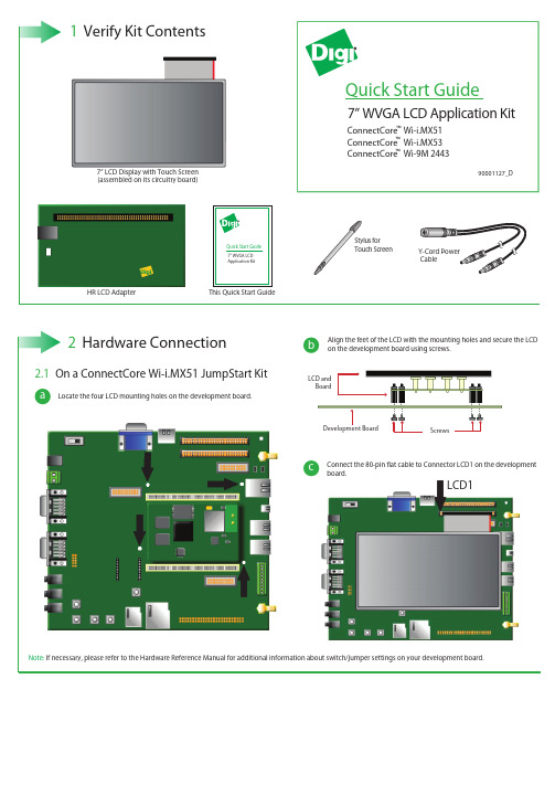
a
3 Download Documentation
a To obtain a materials list and installation instructions speci c to your platform, go to /support/.
90001127_D
HR LCD Adapter
Quick Start Guide 7” WVGA LCD Application Kit
This Quick Start Guide
Stylus for Touch Screen
Y-Cord Power Cable
2 Hardware Connection
c Connect the Y-Cord Power Cable to the JumpStart power supply and its outlets to the JumpStart board (X24) and to the HR LCD Adapter power inlets. b
a
© Digi International, Inc., 2011 Digi, Digi International, the Digi Logo, Digi JumpStart Kit, and ConnectCore are trademarks or registered trademarks of Digi International, Inc., in the United States and other countries worldwide. All other trademarks are property of their respective owners.1Biblioteka Verify Kit Contents
Unitronics SambaOPLC 3.5英寸、4.3英寸和7英寸平板颜色触摸屏PLC说明书
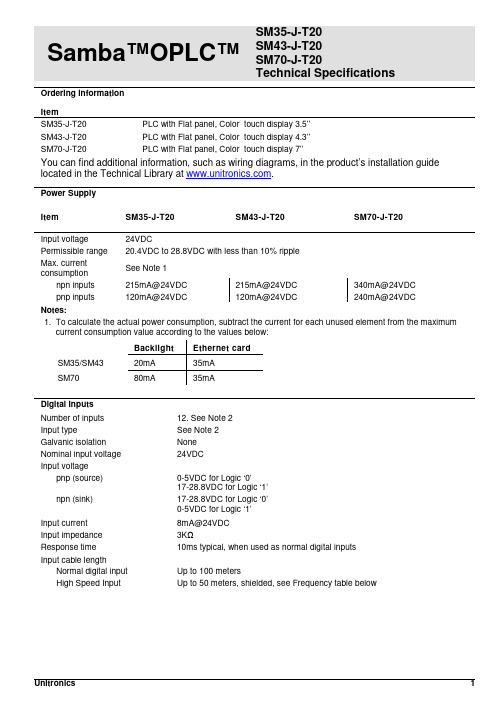
Samba™OPLC™ SM35-J-T20SM43-J-T20SM70-J-T20Technical SpecificationsOrdering InformationItemSM35-J-T20 PLC with Flat panel, Color touch display 3.5’’SM43-J-T20 PLC with Flat panel, Color touch display 4.3’’SM70-J-T20 PLC with Flat panel, Color touch display 7’’You can find additional information, such as wiring diagrams, in the product’s installation guide located in the Technical Library at .Power SupplyItem SM35-J-T20 SM43-J-T20 SM70-J-T20Input voltage 24VDCPermissible range 20.4VDC to 28.8VDC with less than 10% rippleMax. currentconsumptionSee Note 1npn inputs 215mA@24VDC 215mA@24VDC 340mA@24VDCpnp inputs 120mA@24VDC 120mA@24VDC 240mA@24VDCNotes:1. To calculate the actual power consumption, subtract the current for each unused element from the maximumcurrent consumption value according to the values below:Backlight Ethernet cardSM35/SM43 20mA 35mASM70 80mA 35mADigital InputsNumber of inputs 12. See Note 2Input type See Note 2Galvanic isolation NoneNominal input voltage 24VDCInput voltagepnp (source) 0-5VDC for Logic ‘0’17-28.8VDC for Logic ‘1’npn (sink) 17-28.8VDC for Logic ‘0’0-5VDC for Logic ‘1’Input current 8mA@24VDCInput impedance 3KΩResponse time 10ms typical, when used as normal digital inputsInput cable lengthNormal digital input Up to 100 metersHigh Speed Input Up to 50 meters, shielded, see Frequency table below2/15 Samba™ OPLC™High speed inputs Specifications below apply when wired as HSC/shaft-encoder.See Note 2Frequency (max) See Note 3Cable length (max.) HSC Shaft-encoder10m 30kHz 20kHz25m 30kHz 13kHz50m 25kHz 9kHzDuty cycle 40-60%Resolution 32-bitNotes:2. This model comprises a total of 12 inputs. Input functionality can be adapted as follows:12 inputs may be used as digital inputs. They may be wired, in a group, and set to eithernpn or pnp via a single jumper.In addition, according to jumper settings and appropriate wiring:Inputs 10 and 11 can function as either digital or analog inputs.Inputs 0, 2, and 4 can function as high-speed counters, as part of a shaft-encoder,or as normal digital inputs.Inputs 1, 3, and 5 can function as either counter reset, as part of a shaft-encoder,or as normal digital inputs.If inputs 0, 2, 4 are set as high-speed counters (without reset), inputs 1, 3, 5can function as normal digital inputs.3. pnp/npn maximum frequency is at 24VDC.Analog InputsNumber of inputs 2, according to wiring as described above in Note 2Input type Multi-range inputs: 0-10V, 0-20mA, 4-20mAInput range 0-20mA, 4-20mA 0-10VDCInput impedance 243Ω>150KΩMaximum input rating 25mA, 6V 15VGalvanic isolation NoneConversion method Successive approximationResolution (except 4-20mA) 10-bit (1024 units)Resolution (at 4-20mA) 204 to 1023 (820 units)Conversion time One configured input is updated per scan. See Note 4Precision 0.9%Status indication Yes – if an analog input deviates above the permissible range,its value will be 1024.Note:4. For example, if 2 inputs are configured as analog, it takes 2 scans to update all analog values.SMxx-J-T20 Technical Specifications 2/15Digital OutputsNumber of outputs 8 transistor pnp (source)Output type P-MOSFET (open drain)Isolation NoneOutput current (resistive load) 0.5A maximum per output3A maximum total per commonMaximum frequency 50Hz (resistive load)0.5Hz (inductive load)PWM maximum frequency 0.5KHz (resistive load). See Note 5Short circuit protection YesShort circuit indication Via softwareOn voltage drop 0.5VDC maximumPower supply for outputsOperating voltage 20.4 to 28.8VDCNominal voltage 24VDCNote:5. Outputs 0 to 6 can be used as PWM outputs.Graphic Display ScreenItem SM35-J-T20 SM43-J-T20 SM70-J-T20 LCD Type TFT, LCD display TFT, LCD display TFT, LCD display Illumination backlight White LED White LED White LED Display resolution 320x240 pixels 480x272 pixels 800x480 pixels Viewing area 3.5" 4.3" 7"Colors 65,536 (16-bit) 65,536 (16-bit) 65,536 (16-bit) Touchscreen Resistive, analog Resistive, analog Resistive, analog Screen brightness control Via software (Store value to SI 9, values range: 0 to 100%)Virtual Keypad Displays virtual keyboard when the application requires data entry.ProgramItem SM35-J-T20 SM43-J-T20 SM70-J-T20 Memory sizeApplication Logic 112KB 112KB 112KBImages 1MB 2MB 5MBFonts 512KB 512KB 512KBOperand type Quantity Symbol ValueMemory Bits 512 MB Bit (coil)Memory Integers 256 MI 16-bit signed/unsignedLong Integers 32 ML 32-bit signed/unsignedDouble Word 32 DW 32-bit unsignedMemory Floats 24 MF 32-bit signed/unsignedFast Bits 64 XB Fast Bits (coil) – not retainedFast Integers 32 XI 16 bit signed/unsigned (fast, not retained)Fast Long Integers 16 XL 32 bit signed/unsigned (fast, not retained)Fast Double Word 16 XDW 32 bit unsigned (fast, not retained)Timers 32T Res. 10 ms; max 99h, 59 min, 59.99sCounters 16 C 32-bitData Tables 32K dynamic data (recipe parameters, datalogs, etc.)16K fixed data (read-only data, ingredient names, etc)HMI displays Up to 24Program scan time 15µs per 1kb of typical application2/15 Samba™ OPLC™Communication PortsPort 1 1 channel, RS232 (SM35) , USB device (SM43/SM70)Galvanic isolation SM35 and SM43 – NoSM70 - YesBaud rate 300 to 115200 bpsRS232 (SM35 only)Input voltage ±20VDC absolute maximumCable length 15m maximum (50’)USB device (SM43,SM70 only)Port type Mini-BSpecification USB 2.0 complaint; full speedCable USB 2.0 complaint; up to 3mPort 2 (optional) See Note 6CANbus (optional) See Note 6Notes:6. The user may order and install one or both of the following modules:- A serial RS232/RS485 isolated/non-isolated interface module, or an Ethernet Interface module in port 2.- A CANbus modulemodules documentation is available on the Unitronics website.MiscellaneousClock (RTC) Real-time clock functions (date and time)Battery back-up 7 years typical at 25°C, battery back-up for RTC and system data, includingvariable dataBattery replacement Yes. Coin-type 3V, lithium battery, CR2450DimensionsItem SM35-J-T20 SM43-J-T20 SM70-J-T20Size 109 x 114.1 x 68mm(4.29 x 4.49 x 2.67”).See Note 7 136 x 105.1 x 61.3mm(5.35 x 4.13 x 2.41”).See Note 7210 x 146.4 x 42.3mm(8.26 x 5.76 x 1.66”).See Note 7Weight 205g (7.23 oz) 344g (12.13 oz) 633g (22.32 oz) Notes:7. For exact dimensions, refer to the product’s Installation Guide.EnvironmentOperational temperature 0 to 50ºC (32 to 122ºF)Storage temperature -20 to 60ºC (-4 to 140ºF)Relative Humidity (RH) 10% to 95% (non-condensing)Mounting method Panel mounted (IP65/66/NEMA4X)DIN-rail mounted (IP20/NEMA1)Operating Altitude 2000m (6562 ft)Shock IEC 60068-2-27, 15G, 11ms durationVibration IEC 60068-2-6, 5Hz to 8.4Hz, 3.5mm constant amplitude,8.4Hz to 150Hz, 1G acceleration.SMxx-J-T20 Technical Specifications 2/15 The information in this document reflects products at the date of printing. Unitronics reserves the right, subject to all applicable laws, at any time, at its solediscretion, and without notice, to discontinue or change the features, designs, materials and other specifications of its products, and to either permanently ortemporarily withdraw any of the forgoing from the market.All information in this document is provided "as is" without warranty of any kind, either expressed or implied, including but not limited to any implied warranties of merchantability, fitness for a particular purpose, or non-infringement. Unitronics assumes no responsibility for errors or omissions in the information presented inthis document. In no event shall Unitronics be liable for any special, incidental, indirect or consequential damages of any kind, or any damages whatsoever arising out of or in connection with the use or performance of this information.The tradenames, trademarks, logos and service marks presented in this document, including their design, are the property of Unitronics (1989) (R"G) Ltd. or other third parties and you are not permitted to use them without the prior written consent of Unitronics or such third party as may own them.DOC17017-A8 02/15。
芯驿 ax7z010b 开发板 用户手册说明书
文档版本控制目录文档版本控制 (2)一、开发板简介 (6)二、AC7Z010核心板 (8)(一)简介 (8)(二)ZYNQ芯片 (9)(三)DDR3 DRAM (11)(四)QSPI Flash (14)(五)时钟配置 (16)(六)电源 (17)(七)结构图 (18)(八)连接器管脚定义 (19)三、扩展板 (23)(一)简介 (23)(二)CAN通信接口 (24)(三)485通信接口 (24)(四)千兆以太网接口 (25)(五)USB2.0 Host接口 (27)(六)USB转串口 (28)(七)AD输入接口 (29)(八)HDMI输出接口 (30)(九)MIPI摄像头接口(仅AX7Z020使用) (32)(十)SD卡槽 (33)(十一)EEPROM (34)(十二)实时时钟 (34)(十三)温度传感器 (35)(十四)JTAG接口 (36)(十五)用户LED灯 (36)(十六)用户按键 (37)(十七)扩展口 (38)(十八)供电电源 (40)(十九)底板结构图 (41)芯驿电子科技(上海)有限公司 基于XILINX ZYNQ7000开发平台的开发板(型号: AX7Z010B )2022款正式发布了,为了让您对此开发平台可以快速了解,我们编写了此用户手册。
这款ZYNQ7000 FPGA 开发平台采用核心板加扩展板的模式,方便用户对核心板的二次开发利用。
核心板使用XILINX 的Zynq7000 SOC 芯片的解决方案,它采用ARM+FPGA SOC 技术将双核ARM Cortex-A9 和FPGA 可编程逻辑集成在一颗芯片上。
另外核心板上含有2片共512MB 高速DDR3 SDRAM 芯片和1片256Mb 的QSPI FLASH 芯片。
在底板设计上我们为用户扩展了丰富的外围接口,比如2路CAN 通信接口,2路485通信接口,2路XADC 输入接口, 1路千兆以太网接口,1路USB2.0 HOST 接口,1路HDMI输出接口,Uart 通信接口,SD 卡座,40针扩展接口等等。
河西电子7英寸TFT显示模块说明书
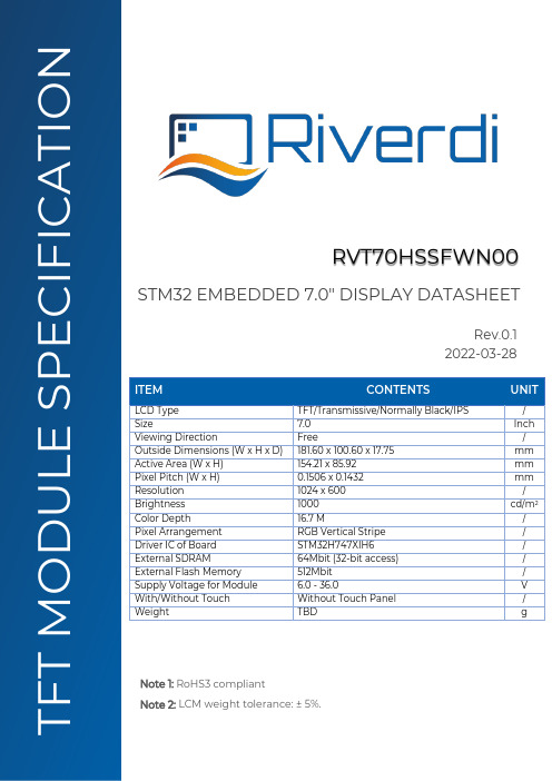
ITEM CONTENTS UNIT LCD Type TFT/Transmissive/Normally Black/IPS / Size 7.0 Inch Viewing Direction Free / Outside Dimensions (W x H x D) 181.60 x 100.60 x 17.75 mm Active Area (W x H) 154.21 x 85.92 mm Pixel Pitch (W x H) 0.1506 x 0.1432 mm Resolution 1024 x 600 / Brightness 1000 cd/m 2 Color Depth 16.7 M / Pixel Arrangement RGB Vertical Stripe / Driver IC of Board STM32H747XIH6 / External SDRAM 64Mbit (32-bit access) / External Flash Memory 512Mbit / Supply Voltage for Module 6.0 - 36.0 V With/Without Touch Without Touch Panel / Weight TBD g STM32 EMBEDDED 7.0" DISPLAY DATASHEET RVT70HSSFWN00 Rev.0.1 2022-03-28 F T M O D U L E S P E C I F I C A T I O N Note 1: RoHS3 compliant Note 2: LCM weight tolerance: ± 5%.REVISION RECORDREV NO. REV DATE CONTENTS REMARKS0.1 2022-03-28 Preliminary versionCONTENTSREVISION RECORD (2)CONTENTS (3)MODULE CLASSIFICATION INFORMATION (4)ASSEMBLY GUIDE (5)MODULE DRAWING (6)ABSOLUTE MAXIMUM RATINGS (7)ELECTRICAL CHARACTERISTICS (7)BACKLIGHT ELECTRICAL CHARACTERISTICS (7)ELECTRO-OPTICAL CHARACTERISTICS (8)BOARD INTERFACES AND CONNECTORS (10)USER INTERFACES (16)DISPLAY SEPCIFICATION (17)INSPECTION (17)RELIABILITY TEST (19)LEGAL INFORMATION (20)MODULE CLASSIFICATION INFORMATIONRV T 70 H S S F W N 00 1. 2. 3. 4. 5. 6. 7. 8. 9. 10.ASSEMBLY GUIDEMounting frameFor dimensions 3.5”, 4.3”, 5.0”, 7.0” and 10.1”, the product with mounting frame version is available. Thanks to the four catches attached to the side, frame provides strong assembly to the surface by mounting element (like the screw, see Figure 1). The frames are specially designed to fit Riverdi products perfectly. The diameter of the mounting hole is 3.5mm.Figure 1. Mounting frameABSOLUTE MAXIMUM RATINGSPARAMETER SYMBOL MIN MAX UNIT NOTESupply Voltage for Module VDD 0.0 48.0V Note 1Digital I/O signals Voltage - -0.5 3.3 Note 1,2Operating Temperature T OP-20 70 °CStorage Temperature T ST-30 80 °CStorage Humidity (@ 25 ± 5°C) H ST10 - % RHOperating Ambient Humidity (@ 25 ± 5°C) H OP10 - % RHNote 1. Exceeding maximum values may cause improper operation or permanent damageto the unit.Note 2. Most of the GPIOs have the 5.0 V tolerant input voltage, please refer to the datasheetof STM32H747XIH6 for more details.ELECTRICAL CHARACTERISTICSPARAMETER SYMBOL MIN TYP MAX UNIT Supply Voltage for Module VDD_IN 6.0 12.0 36.0 VPOWER‘ENABLE’ = ‘0’***************************I VDD_IN=6.0 V TBD TBD TBD uA ****************************I VDD_IN=12.0 V TBD TBD TBD uA ****************************I VDD_IN=24.0 V TBD TBD TBD uA ****************************I VDD_IN=36.0 V TBD TBD TBD uAPOWER‘ENABLE’ = ‘1’***************************I VDD_IN=6.0 V TBD TBD TBD mA ****************************I VDD_IN=12.0 V TBD TBD TBD mA ****************************I VDD_IN=24.0 V TBD TBD TBD mA ****************************I VDD_IN=36.0 V TBD TBD TBD mAInput Voltage “H” Level V IH 2.0 - 3.3 V Input Voltage “L” Level V IL 0 - 0.8 V Note. POWER ‘ENABLE’ refers to pin 4, ‘ENABLE’ of the power input connector(P2).By default, POWER ‘ENABLE’ = ‘1’,When POWER ‘ENABLE’ = ‘0’, the device is turned off.BACKLIGHT ELECTRICAL CHARACTERISTICSPARAMETER SYMBOL MIN TYP MAX UNIT NOTE Lifetime - - 50,000 - hours Note 1Note 1. Operating life means the period in which the LED brightness goes down to 50% ofthe initial brightness. Typical operating lifetime is the estimated parameter.ELECTRO-OPTICAL CHARACTERISTICSITEM SYMBOL CONDITION MIN TYP MAX UNIT RMK NOTEResponse Time Tr+Tfθ=0°∅=0° - 35 35 ms FIG 2. 4Contrast Ratio Cr 800 1000 - --- FIG 3. 1 Luminance δ- 75 - % FIG 3. 3 Figure 3.Contrast Ratio =Average Surface Luminance with all white pixels (P1,P2,P3,P4,P5) Average Surface Luminance with all black pixels (P1,P2,P3,P4,P5)Note 2.Surface luminance is the LCD surface from the surface with all pixels displaying white. For more information see Figure 3.Lv = Average Surface Luminance with all white pixels (P1, P2, P3, P4, P5)Note 3.The uniformity in surface luminance δWHITE is determined by measuring luminance at each test position 1 through 5, and then dividing the minimum luminance of 5 points luminance by maximum luminance of 5 points luminance. For more information see Figure 3.δ WHITE =Minimum Surface Luminance with all white pixels (P1,P2,P3,P4,P5) Maximum Surface Luminance with all white pixels (P1,P2,P3,P4,P5)Note 4. Response time is the time required for the display to transition from white to black (Rise Time, Tr) and from black to white (Decay Time, Tf). For additional information see Figure 2. The test equipment is Autronic-Melchers’s ConoScope series.Note 5. CIE (x, y) chromaticity, the x, y value is determined by measuring luminance at each test position 1 through 5, and then calculating the average value.Note 6. Viewing angle is the angle at which the contrast ratio is greater than 2. For TFT module the contrast ratio is greater than 10. The angles are determined for the horizontal or x axis and the vertical or y axis with respect to the z axis which is normal to LCD surface. For more information see Figure 4.Note 7. For viewing angle and response time testing, the testing data is based on Autronic-Melchers’s ConoScope series. Instruments for Contrast Ratio, Surface Luminance, Luminance Uniformity, CIE the test data is based on TOPCON’s BM-5 photo detector.Figure 2. The definition of response timeFigure 3. Measuring method for Contrast ratio, surface luminance, Luminance uniformity, CIE (x, y) chromaticityA: 5mmB: 5mmH, V: Active AreaLight spot size ∅=5mm, 500mm distancefrom the LCD surface to detector lens.Measurement instrument is TOPCON’Sluminance meter BM-5Figure 4. The definition of viewing angleBOARD INTERFACES AND CONNECTORSPower input connectorThe 1.25mm, 6-pin Molex connector labeled as “POWER’ (P2) is power input connector. There is an internal reverse polarity protection which ensures that the device is not damaged if the power supply polarity is reversed.NO. PIN DESCRIPTION NOTE1 VDD_IN Power supply input; 6.0-36.0VNote 12 VDD_IN Power supply input; 6.0-36.0V3 VDD_IN Power supply input; 6.0-36.0V4 ENABLE Enable/ Disable power supply. Note 25 GND Ground6 GND GroundNote 1: STM32 Embedded Display allows to directly connect one additional display to the system. There is RiBUS connector on the board where you can connect any of intelligent display from Riverdi based on EVE4 (BT817Q). However, please note that it may change power supply requirement as below:The power supply voltage must range between 7.0V- 14.0 V (TYP. 9.0 V), if Riverdi EVE4 10.1” series display is connected through RiBUS. At the same time, jumper P5 shall be configured according to subchapter 10.8, note 1.The power supply voltage ranges between 6.0 V- 36.0V if any of Riverdi EVE4 3.5”,4.3”,5.0” and 7.0” series display is connected through RiBUS. At the same time, jumper P12 shall be configured according to subchapter 10.8, note 1.Note 2: By default, pin “ENABLE” is pulled up to VDD and enabled. To disable, ground the pin to turn off the device completely.USB interfaceThe 1.25mm, 5-pin Molex connector labeled as “USB’ (P10) is USB interface.NO. PIN DESCRIPTION NOTE1 VCC_USB Power supply2 D- USB data-3 D+ USB data+4 ID USB OTG ID; Host /Device detect Note 15 GND GroundNote 1. Configuration of the USB Host/Device mode:Host Mode: Pin 4 (ID) should be connected to GND.In this mode, it can provide +5V output voltage to the connected USB device and Max output current 500 mA.Device Mode: Pin 4 (ID) should be not connected (floating).RS485 interfaceThe 1.25mm, 4-pin Molex connector labeled as “RS485’ (P3) is RS485 interface.NO. PIN DESCRIPTION NOTE1 VDD_IN Power supply input; 6.0-36.0V2 A Non-inverting receiver input and non-inverting driver output3 B Inverting receiver input and inverting driver output4 GND GroundRS232 interfaceThe 1.25mm, 5-pin Molex connector labeled as “RS232’ (P1) is RS232 interface.NO. PIN DESCRIPTION NOTE1 RTS Request to send2 CTS Clear to send3 TXD Transmit Data4 RXD Receive Data5 GND Ground2 x CAN FD interfacesThe main board supports 2 channels of the CANFD (Control Area Network Flexible Data-Rate) communication bus, based on the high-speed (2.5-8.0Mbps) CAN transceiver.2 pcs of 1.25mm, 4-pin Molex connectors labeled as “CAN1’ (P11) and “CAN2” (P15) are respectively interfaces of CAN FD1 and CAN FD2.NO. PIN DESCRIPTION NOTE1 GND Ground2 CAN_L CAN Low-Level Voltage3 CAN_H CAN High-Level Voltage4 VDD_IN Power supply input; 6.0 – 36.0 VHaptic feedback connectorThe 1.25mm, 2-pin Molex connector labeled as “HAPTIC’ (P7) is haptic feedback connector. Haptic feedback P7 is used to connect with the haptic motor directly.NO. PIN DESCRIPTION NOTE1 OUT- Negative haptic driver differential outputNote 12 OUT+ Positive haptic driver differential outputNote 1: The haptic driver DRV2605L is controlled directly by I2C protocolSWD (Serial Wire Debug) connectorThe 1.25mm, 6-pin Molex connector labeled as ‘SWD’ (P6) is SWD interface, which is used for programing the MCU on board.NO. PIN DESCRIPTION NOTE1 VCC_+3.3V Power input2 SW_CLK Serial wire clock3 GND Ground4 SW_DIO Serial wire debug data input/output5 RST Reset; Active low6 SWO Serial wire trace outputRiBUSAny size of the Riverdi EVE4 series display can be connected through RiBUS to act as a slave module to the mainboard.NO. PIN DESCRIPTION NOTE1 VCC_+3.3V Supply voltage for module; TYP3.3Vbetween 7.0 - 14.0V (TYP. 9V).For Riverdi EVE4 series display ranging from sizes of 3.5” to 7.0”, the backlight voltage (BLVDD) shall be 5.0V.Backlight jumper selectors, P5 and P12, labeled as “BLVDD SEL EXT”and “BLVDD SEL INT are used to configure the backlight voltage range.Warning! Jumper configuration shall be done when module is not powered.DO NOT change ANY jumpers while the module has power. Improper operation might cause permanent damage to the unit.Please pay special attention to not misplace the jumpers. Incorrect jumpers setting may lead to damage to the module as well.The P5, P12 jumpers setting are shown below.Table 1. Internal backlight selector P12 setting: 5.0V (default) backlight voltageSETTING P5, PIN 1 &2P5, PIN 3 &4P12, PIN 1 &2P12, PIN 3 &45.0V (Default) Open Open Short ShortTable 2. External backlight selector P5 setting: 7.0V-14.0V backlight voltageSETTING P5, PIN 1 &2P5, PIN 3 &4P12, PIN 1 &2P12, PIN 3 &47.0V - 14.0 V Short Short Open OpenExpansion connectorThe main board has one 1.27mm, 40-pin expansion pin header which is labeled as “EXPANSION CONNECTOR’ (P8).It provides direct access to below GPIOs of MCU STM32H747XIH6,which make it possible to easily extend a daughterboard for a specific application.• 2 x I2C• 1 x UART• 1 x USART• 1 x SPI• 1 x USB•7 x PWMs• 2 x DACs (Digital-to-analog)• 2 x ADCs (Analog-to-digital)Each of the GPIO pins can be configured by software as output (push-pull or open-drain, with or without pull-up or pull-down), as input (floating, with or without pull-up or pull-down) or as peripheral alternate function. Most of the GPIO pins are shared with digital or analog alternate functions. Please refer to the datasheet of MCU STM32H747XIH6 for more details.I/O/P PIN NAME NO. NO. PIN NAME I/O/PP VCC_+5V 1 2 VCC_+3.3V PP VCC_+5V 3 4 VCC_+3.3V PI/O PA5 5 6 GND PP GND 7 8 PA4 I/OI/O PE4 9 10 PD11 I/OI/O PK1 11 12 PB10 I/OI/O PD12 13 14 PC7 I/OI/O PD13 15 16 PA3 I/OP GND 17 18 GND PI/O PC2 19 20 PA0_C I/OI/O PC3 21 22 PA1_C I/OI/O PA12 23 24 PC2_C I/OI/O PA9 25 26 PC3_C I/OI/O PA10 27 28 GND PI/O PJ8 29 30 PC13 I/OI/O P18 31 32 PA8 I/OI/O PJ10 33 34 PB11 I/OI/O PB0 35 36 PH4 I/OI/O PC6 37 38 PB12 I/OI/O PB14 39 40 PB15 I/ONote 1. ***************************from pin 1 and pin3 is maximum 1A.********************************************************.Note 2.The ‘USR LED’ is connected to pin 33, PJ10, of the expansion connector.By default, the resistor R60, (0402, 1k ohms) is soldered. Please remove R60 to useGPIO channel PJ10.Note 3. Push button BTN2(S2) is connected to pin 35, PB0, of the expansion connector. Please remove R58 to use GPIO channel PB0.Push button BTN1(S1) is connected to pin 37, PC6, of the expansion connector.Please remove R57 to use GPIO channel PC6.Micro SD slotThe mainboard is equipped with Micro-SD slot, which supports all types of Micro SD cards.2 x 20-pin, 1.27 mm pin sockets for POE Add-on BoardThe 2 x 20-pin, 1.27 mm, pin sockets, labeled as U9a and U9b, are used to connect the Riverdi POE Add-on Board.The Riverdi POE Add-on Board features 10/100M Ethernet Port with Power-Over-Ethernet enabled. It allows you to power the module through the Ethernet port.Note. The Riverdi POE Add-on Board is offered as an accessory.USER INTERFACES3 x push buttonsPush button labeled as “RST” is used to “RESET” the module.Another 2 push buttons labeled as BTN1, BTN2 are for user’s development.•BTN1(S1) is connected to pin 37, PC6, of the expansion connector.•BTN2(S2) is connected to pin 35, PB0, of the expansion connector.By default, pushbuttons BTN1(S1), BTN2(S2) are enabled. To use GPIO channel PC6 and PB0, R57 and R58 should be removed.3 x LEDs1 x LED, labeled as ‘PWR LED’, emits green light when the modules is powered.1 x LED, labeled as ‘USB OVR’, emits red light when VCC_USB pin is shorted.1 x LED, labeled as ‘USR LED’, is for user’s development.•The ‘USR LED’ is connected to pin 33, PJ10, of the expansion connector.By default, the resistor R60, (0402, 1k ohms) is soldered. Please remove R60 to use GPIO channel PJ10.D ISPLAY SEPCIFICATIONTFT resolutionThe supported resolution of the display in this module is 1024*600.Full TFT specificationFor detailed information on the display, please refer to datasheet of displayRVT70HSMFWN00.I NSPECTIONStandard acceptance/rejection criteria for TFT moduleInspection conditionAmbient conditions:•Temperature: 25 ± 2°C•Humidity: (60 ± 10) %RH•Illumination: Single fluorescent lamp non-directive (300 to 700 lux) Viewing distance: 35 ± 5cm between inspector bare eye and LCD.Viewing Angle: U/D: 45°/45°, L/R: 45°/45°Inspection standardITEM CRITERIONBlack spots,white spots,light leakage,Foreign Particle(round Type)D=(x+y)/2Spot’s density: 10 mmSize = 7”Average Diameter Qualified QtyD ≤ 0.2 mm Ignored0.2 mm < D ≤ 0.3 mm N≤30.5mm < D Not allowed 0.5mm < DLCD black spots, white spots, light leakage (line Type)Size = 7”Length Width Qualified Qty - W ≤ 0.05IgnoredL ≤ 5.00.05 < W ≤ 0.1 35.0 < L 0.1 < W Not allowedBright/Dark DotsSize = 7”Item Qualified Qty Bright dots N≤2Dark dots N≤3 Total bright and dark dots N≤4Clear spotsSize = 7”Average Diameter Qualified QtyD < 0.2 mm Ignored0.2 mm < D < 0.3 mm 40.3 mm < D < 0.5 mm 20.5 mm < D 0Polarizer bubblesSize = 7”Average Diameter Qualified QtyD ≤ 0.2 mm Ignored0.2 mm < D ≤ 0.5 mm 40.5 mm < D 0Touch panel spotSize ≥ 5"Average Diameter Qualified QtyD < 0.25 mm Ignored0.25 mm < D < 0.5 mm 40.5 mm < D 0Touch panel White line ScratchSize ≥ 5’’Length Width Qualified Qty - W < 0.03 IgnoredL < 5.0 0.03 < W < 0.05 2- 0.05 < W 0RELIABILITY TESTNO.TEST ITEMTEST CONDITIONNOTE1 High Temperature Storage 80°C/120 hoursNote 12 Low Temperature Storage -30°C/120 hours3 High Temperature Operating 70 °C /120 hours Note 2. Before cosmetic and function test, the product must have enough recovery time, at least 2 hours at room temperature.L EGAL INFORMATIONRiverdi grants the guarantee for the proper operation of the goods for a period of 12 months from the date of possession of the goods. If in a consequence of this guaranteed execution the customer has received the defects-free item as replacement for the defective item, the effectiveness period of this guarantee shall start anew from the moment the customer receives the defects-free item.Information about device is the property of Riverdi and may be the subject of patents pending or granted. It is not allowed to copy or disclosed this document without prior written permission.Riverdi endeavors to ensure that all contained information in this document is correct but does not accept liability for any error or omission. Riverdi products are in developing process and published information may be not up to date. Riverdi reserves the right to update and makes changes to Specifications or written material without prior notice at any time. It is important to check the current position with Riverdi.Images and graphics used in this document are only for illustrative the purpose. All images and graphics are possible to be displayed on the range products of Riverdi, however the quality may vary. Riverdi is no liable to the buyer or to any third party for any indirect, incidental, special, consequential, punitive, or exemplary damages (including without limitation lost profits, lost savings, or loss of business opportunity) relating to any product, service provided or to be provided by Riverdi, or the use or inability to use the same, even if Riverdi has been advised of the possibility of such damages.Riverdi products are not fault tolerant nor designed, manufactured or intended for use or resale as on line control equipment in hazardous environments requiring fail–safe performance, such as in the operation of nuclear facilities, aircraft navigation or communication systems, air traffic control, direct life support machines or weapons systems in which the failure of the product could lead directly to death, personal injury or severe physical or environmental damage (‘High-Risk Activities’). Riverdi and i ts suppliers specifically disclaim any expressed or implied warranty of fitness for High-Risk Activities. Using Riverdi products and devices in 'High-Risk Activities' and in any other application is entirely at the buyer’s risk, and the buyer agrees to def end, indemnify, and hold harmless Riverdi from all damages, claims or expenses resulting from such use. No licenses are conveyed, implicitly or otherwise, under any Riverdi intellectual property rights.。
MAGIC2103-ARM7开发板II用户手册_v1.00
MAGIC2103-ARM7开发板II 用 户 手册版 本 号: v1.00技术支持QQ : 571097167公 司 : 模数科技公 司 主 页 :日 期 : 2008.2.22目 录一、 MAGIC2103-ARM7开发板简介 (3)二、 套件清单 (3)三、 实例程序清单(拥有ADS1.2和Keil uVision3双环境例程) (4)四、 硬件资源 (4)五、 光盘内容 (5)六、 开发板资源分布图 (5)七、 接口说明 (6)八、 工具软件介绍 (6)< 一 > ADS1.2集成开发环境 (6)1、 简介 (6)2、 安装 (6)3、 使用 (6)< 二 > H-JTAG 调试助手 (6)1、 ARM7 JTAG下载线简介 (6)2、 H-JTAG安装 (7)3、 H-JTAG配置 (9)4、 H-JTAG使用方法 (12)< 三 > Keil uVision3集成开发环境 (13)< 四 > Flash Magic下载软件 (16)九、 后记 (17)一、M AGIC2103-ARM7开发板简介MAGIC2103-ARM7开发板II是在MAGIC2103-ARM7开发板的基础上升级而来,弥补了一下缺陷,外扩了I/O口和ADC输入接口。
它采用PHILIPS公司最新推出的基于ARM7TDMI-S 、LQFP48封装的LPC2103,最高工作速度可达70MHz(63MIP),8K的片内静态RAM和32KB的片内FLASH程序存储器。
通过ISP或JTAG实现程序下载和调试。
关于芯片的详细特性请见《LPC2101_2102_2103 ARM 微控制器数据手册》和《LPC2101_2102_2103 ARM微控制器使用指南》。
为适应广大用户的不同需求,MAGIC2103开发板提供了如今最流行的ADS1.2和Keil uVision3两种集成开发环境,并配备了20个经典的实例程序和详细的实例教程,使上手更加容易,快速完成51到ARM的过渡!二、套件清单◇ MAGIC2103-ARM7开发板一块◇ ARM JTAG下载线一个◇ 并口延长线一根◇ 串口延长线一根◇ USB电源线一根◇ 配套光盘一张三、实例程序清单(拥有ADS1.2和Keil uVision3双环境例程)实例01、GPIO实验-熟悉开发环境,以及程序下载和调试实例02、GPIO实验-流水灯与蜂鸣器演示实例03、高速GPIO实验-闪灯演示实例04、GPIO输入实验-按键控制实例05、PWM实验-LED控制实例06、定时器中断实验-向量中断实例07、定时器中断实验-非向量中断实例08、WDT看门狗实验实例09、电源管理之空闲模式实例10、电源管理之掉电模式实例11、UART1通信实验-查询方式接收实例12、UART0通信实验-中断方式接收实例13、IIC实验-EEPROM读写实例14、重映射实验实例15、GPIO模拟总线实验-LCD1602液晶显示实例16、ADC实验-千分之一精度电压表实例17、RTC实验-万年历电子钟实例18、EINT外部中断实验-PS/2键盘打字练习器实例19、基于uCOS-II 2.52的GPIO读写实验(基于ADS1.2集成开发环境)实例20、基于uCOS-II 2.52的ADC实验-千分之一精度电压表(基于ADS1.2集成开发环境)四、硬件资源◇ LPC2103(PHILIPS)ARM7TDMI-S,最高频率可达70MHz,片内8K SRAM,32K FLASH◇ EEPROM (24LC04)◇ 两个三线RS232接口,其中一个可用作ISP◇ 复位监控芯片SP708S◇ 3个独立按键◇ 1个蜂鸣器◇ LCD1602字符液晶◇ PS/2键盘接口◇ 可调电阻(ADC模拟信号输入)◇ 20芯ARM JTAG下载口◇ 3.3V、1.8V电源模块◇ 3个LED指示灯◇ USB电源接口◇ 系统晶振11.0592MHz◇ 11位I/O扩展口◇ 1位ADC输入口五、光盘内容◇ Keil uVision3集成开发环境◇ ADS1.2集成开发环境◇ H-JTAG 调试助手◇ Flash Magic下载软件◇ MAGIC2103-ARM7开发板ADS1.2实例包◇ MAGIC2103-ARM7开发板Keil uVision3实例包◇ MAGIC2103-ARM7开发板用户手册◇ MAGIC2103-ARM7开发板实例祥解◇ MAGIC2103-ARM7开发板原理图◇ MAGIC2103-ARM7开发板简介◇ LPC2103 LPC2101_2102_2103 ARM微控制器数据手册◇ LPC2101_2102_2103 ARM微控制器使用指南◇ ADS1.2中文教程◇ μCOS-II详解中文版◇ 其它芯片资料六、开发板资源分布图七、接口说明1、调试跳线:当使用JTAG调试时,需要短接此跳线,具体操作见用户手册和实例手册。
KE17Z硬件开发者指南说明书

NXP Semiconductors Document identifier: KE17ZHDG User Guide Rev. 0.1, 13 December 2021KE17Z Hardware Developer's GuideContentsChapter 1 Overview (3)Chapter 2 Power Supply (6)Chapter 3 Clock Module (8)Chapter 4 Reset Circuit (10)Chapter 5 Debug and Programming Interface (11)Chapter 6 Touch Sensing Input (12)Chapter 7 ADC Input Circuit (14)Chapter 8 Digital GPIO and Unused Pin (16)Chapter 9 General Board Layout Guidelines (17)Appendix A Revision History (18)Chapter 1OverviewThis document provides board-level hardware design guidelines for the KE17Z family products (see table). The hardware design guidelines are similar for this product family. In this document, the MKE17Z256VLL7 device is used for demonstration purposes. Table 1.KE17Z family1.INT: interrupt pin numbers; HD: high drive pin numbersKE17Z MCUs extend Kinetis E family to dual TSI performance and broader scalability. Robust and dual TSI provides high-level stability and accuracy to customer's HMI system. 1 Msps ADC and FlexTimer help build a perfect solution for a simple BLDC motor control system.Following are the general features of the KE17Z series MCUs:•Arm® Cortex®-M0+ core, supports up to 72 MHz frequency, with 2.35 CoreMark/MHz.•Scalable memory up to 256 KB program flash and up to 48 KB SRAM• 5 V power supply ranges from 2.7 V to 5.5 V.•Dual capacitive touch sensing modules offer 2 x 25 ch touch sensing channels supporting both self-cap and mutual cap technologies.•Precision mixed-signal capability with 1x high-speed on-chip analog comparator and 1× 12-bit analog-to-digital converter (ADC) with up to 16 channel analog inputs per module, up to 1 Msps.•Flexible timers including 3 × Flex Timers (FTM) for PWM generation, offering up to 8 standard PWM channelsThis document describes the following module and provides appropriate hardware design related recommendations:•Power Supply•Clock Module•Reset Circuit•Debugging and Programming Interface •Touch Sensing interface (TSI)•ADC Input Circuit•Digital GPIO and unused pin •General Board Layout GuidelinesA general schematic example is shown in the following figure.Figure 1.X-KE17Z-TSI-EVB schematic example1.1Related documentationThe table below lists and explains the additional documents and resources that you can refer to for more information on KE17Z MCUs. Some of the documents listed below may be available only under a non-disclosure agreement (NDA). To request access to these documents, contact your local field applications engineer (FAE) or sales representative.Table 2.Related documentationTable continues on the next page...Table 2.Related documentation (continued)Chapter 2Power SupplyThe power supply of KE17Z ranges from 2.7 V to 5.5 V, the detailed operating requirements are listed below. Note that the difference between VDD (digital power supply) and VDDA (analog power supply) cannot exceed 0.1 V, so it is recommended to connect VDD and VDDA directly in practice. Also, the power supply ramp up rate should be limited within 100 V/ms.Table 3.Power supplyThe decoupling capacitors (100 nF as shown in the figure below) are required to filter out the system noise. Figure below shows examples of decoupling capacitors on the schematic, at least one decoupling capacitor per power pin is recommended. On PCB layout level, all decoupling capacitors should be placed as close as possible to each of their respective power supply pin; the ground side of the decoupling capacitor should have a via to the pad which goes directly down to the ground plane. The decoupling capacitors should not route to the power plane through a long trace. The types and values of the decoupling capacitor depend on the noise level and frequency. The typical value is usually in the range of 0.01 μF to 0.1 μF.The bulk capacitor (10 μF as shown in the figure below) acts as a local power supply to the power pin, its typical value is 10 μF.Power SupplyChapter 3Clock ModuleThe KE17Z has the following clock sources:•Fast internal reference clock (FIRC): 48 MHz high-accuracy (up to ±1%) fast internal reference clock (FIRC) for normal Run as the default system clock source after reset.•Slow internal reference clock (SIRC): 8 MHz/2 MHz.•LPFLL: Supports only up to 72 MHz•LPO128K: 128 KHz always on internal low-power oscillator clock, for WDOG, LPTMR, EWM, PORT Control.•External square wave input: Up to 60 MHz DC external square wave input clock•External oscillator clock (OSC): high range 4 - 40 MHz (with low power or high gain mode) and low range 32 - 40 kHz (with high-gain mode only)3.1External oscillator circuit designThe EXTAL and XTAL pins provide the interface for a Crystal oscillator. EXTAL is the input to the crystal oscillator amplifier. XTAL is the output of the crystal oscillator amplifier. The pierce oscillator provides a robust, low-noise, and low-power external clock source. It is designed for optimal start-up margin with typical crystal oscillators. KE17Z supports two ranges of external oscillator:•high-range: 4 - 40 MHz (with low-power or high-gain mode)Table 4.External crystal/resonator connections•low-range: 32 - 40 kHz (with high-gain mode only)The typical circuit design of the external oscillator is shown in the figure below. For the low-power use case, the low-power oscillator mode is recommended, as shown in Diagram 2, thus the 1 Mohm R F (feedback resistor) is not needed in this case. For noise use case, the high-gain oscillator is preferred as shown in Diagram 3. The user needs to add 1 Mohm R F (feedback resistor), also the use needs to double check with the crystal vendor about the exact value of R S (series resistor). The load capacitors of C1 and C2 must be provided by external capacitors and their load capacitance depends on the crystal or resonator manufacturers' recommendation. Check the crystal datasheet for the recommended values. And, also consider the parasitic capacitance of package and board.Figure 2.Crystal circuit design – Diagram 2Clock ModuleFigure 3.Crystal circuit design – Diagram 33.2EMC considerationsAs the clock circuit is very sensitive to the noise, you need to pay attention to the following guidelines on PCB layout:Avoid placing any signal traces close to the clock circuit.Place the external crystal to the EXTAL/XTAL pins as close as possible.A ground area should be placed under the crystal oscillator area. This ground guard ring must be clean ground. This means that no current from and to other devices should be flowing through the guard ring. This guard ring should be connected to VSS with a short trace. Never connect the ground guard ring to any other ground signal on the board. Also avoid implementing ground loops. The following figure shows the recommended placement and routing for the oscillator layout.Chapter 4Reset CircuitResetting the MCU provides a way to start processing from a known set of initial conditions. System reset begins with the on-chip regulator in full regulation and system clocking generation from an internal reference.For all reset sources, the RESET_B pin is driven low by the MCU for at least 128 bus clock cycles and until the flash memory initialization is completed. After flash memory initialization completes, the RESET_B pin is released and the internal chip reset is deasserted. Keeping the RESET_B pin asserted externally delays the negation of the internal chip reset. The detailed boot sequence is shown in the figure above.As shown in the schematic example figure, the reset circuit consists of an external pullup resistor added between reset pin to power supply, a capacitor between the reset pin to ground, and an optional reset button.Debug and Programming InterfaceThis MCU uses the standard Arm SWD interface protocol as shown in the following figure. While pull-up or pull-down resistors are not required (SWD_DIO has an internal pull-up and SWD_CLK has an internal pull-down), external 10 kΩ pull resistors are recommended for system robustness. The RESET_b pin recommendations mentioned above must also be considered.Touch Sensing InputTouch sensing input (TSI) provides touch sensing detection on capacitive touch sensors. The external capacitive touch sensor is typically formed on PCB and the sensor electrodes are connected to TSI input channels through the I/O pins in the device.KE17Z TSI supports dual TSI modules and each TSI module supports two kinds of touch sensing method, the self-capacitive mode and the mutual-capacitive mode.6.1TSI self-capacitive mode design considerationsThe self-capacitive mode requires single pin for each touch sensor and measures the capacitance on an electrode connected to a single TSI channel. It then converts the capacitance into a digital count by driving average current on the electrode and measuring the charge/discharge times.Figure 4.PCB layout of the electrode shapes for TSI self-capacitive modeTo maximize the electrodes area from the capacitor plates, it is recommended that the size of the electrode is similar to a human finger (10×10 mm is considered a good size).6.2TSI mutual capacitive mode design considerationsMutual capacitive mode measures the capacitance between two electrodes connected to two TSI channels. One of the TSI channels is used as transmit (TX) channel and the other one is used as receive (RX) channel.Figure below shows the connections of TSI channel in mutual-capacitive mode.Touch Sensing Input6.3PCB layout of the electrode shapes for TSI mutual capacitive modeThe following figure is the recommended mutual key shape. Note that the number of fingers has much impact on the touch sensitivity. In general, more fingers result in stronger noise immunity but less touch sensitivity. Customer should select the right finger numbers for the thickness of touch overlay. For example, if the touch overlay is 3 mm in thickness, 4 fingers is the best choice. If the touch overlay is 2 mm in thickness, 5 fingers are ok.For the detailed TSI design guide, see KE15ZTSIUG, KE15Z Touch Sensing Interface User Guide.Chapter 7ADC Input CircuitEach ADC input must have an RC filter as shown in the following figure. The maximum value of the resistor must be less than R S (maximum 5 kohm as shown in the table below) if fast sampling and high resolution are required. The value of C must be chosen to ensure that the RC time constant is very small compared to the sample period. For example, the typical filter resistor is 100 ohm, together with the 220 pF capacitor, the low-pass cutoff frequency is 7.238 MHz.The specifications of ADC input impedance and operating conditions are shown below for your reference.Table 5.12-bit ADC operating conditionsTable continues on the next page...ADC Input Circuit Table 5.12-bit ADC operating conditions (continued)1.Typical values assume V DDA = 5 V, Temp = 25 °C, f ADCK = 40 MHz, unless otherwise stated. Typical values are for referenceonly, and are not tested in production.2.DC potential difference.3.For packages without dedicated V REFH and V REFL pins, V REFH is internally tied to V DDA, and V REFL is internally tied to V SSA.4.Clock and compare cycle need to be set according the guidelines in the block guide.5.ADC conversion will become less reliable above maximum frequency.6.When using ADC hardware averaging, refer to the device Reference Manual to determine the most appropriate settingfor AVGS.7.Max ADC conversion rate of 1200 Ksps is with 10-bit modeDigital GPIO and Unused PinFor the detailed IO pin mux functions and pinout, see "Section 4 Pinouts" in KE1xZP100M72SF1, Kinetis KE17Z/13Z/12Z with up to 256 KB Flash Data Sheet.Regarding IO drive strength, there are 8 high drive pins with 20 mA drive strength. These high drive pins are: PTD0, PTD1, PTD15, PTD16, PTB4, PTB5, PTE0, and PTE1. In practice, keep the total output current for all ports under 100 mA as specified in Data Sheet.Regarding the switching terms, the minimum positive voltage applied to the input which will be accepted by the device as a logic high (V IH) is 0.7*VDD, and the maximum positive voltage applied to the input which will be accepted by the device as a logic low (V IL) is 0.3*VDD. They are also listed in the Data Sheet.On reset, the most digital GPIOs (excepting debugging pins) are Disabled/Hi-z by default.8.1EMC considerationsThe general IO block diagram is shown below. As port E supports the glitch filter feature, it’s recommended to use port E pins as the digital input pins, with better noise immunity by enabling the glitch filter feature.There is a pair of ESD protecting diodes on each IO pin, so the user doesn’t need to add the extra ESD diode.8.2NMI pin considerationsAfter reset, the default function of PTD3 pin is NMI (no mask interrupt, low active). The software can configure the pin as other functions only after the reset completes and begins to execute the application code. Therefore, note that the NMI pin cannot be low level at reset, otherwise the code will be stuck in NMI interrupt service routine. In practice, keep the NMI pin unused and unconnected (or pull up with 4.7 kohm resistor) if there is enough pin to use.8.3Unused pin considerationsIn order to improve EMC noise immunity and reduce the current consumption, the used pins are suggested to keep unconnected and the software should configure these unused pins as DISABLED, which is the default pin status after reset.General Board Layout GuidelinesFor the detailed general board layout guidelines, see "Chapter 10" in AN5426, Hardware Design Guidelines for S32K1xx Microcontrollers.Appendix ARevision HistoryThe table below summarizes the revisions to this document. Table 6.Revision historyHow To Reach Us Home Page: Web Support: /support Limited warranty and liability — Information in this document is provided solely to enable system and software implementers to use NXP products. There are no express or implied copyright licenses granted hereunder to design or fabricate any integrated circuits based on the information in this document. NXP reserves the right to make changes without further notice to any products herein.NXP makes no warranty, representation, or guarantee regarding the suitability of its products for any particular purpose, nor does NXP assume any liability arising out of the application or use of any product or circuit, and specifically disclaims any and all liability, including without limitation consequential or incidental damages. “Typical” parameters that may be provided in NXP data sheets and/or specifications can and do vary in different applications, and actual performance may vary over time. All operating parameters, including “typicals,” must be validated for each customer application by customer's technical experts. NXP does not convey any license under its patent rights nor the rights of others. NXP sells products pursuant to standard terms and conditions of sale, which can be found at the following address: /SalesTermsandConditions.Right to make changes - NXP Semiconductors reserves the right to make changes to information published in this document, including without limitation specifications and product descriptions, at any time and without notice. This document supersedes and replaces all information supplied prior to the publication hereof.Security — Customer understands that all NXP products may be subject to unidentified or documented vulnerabilities. Customeris responsible for the design and operation of its applications and products throughout their lifecycles to reduce the effect of these vulnerabilities on customer’s applications and products. Customer’s responsibility also extends to other open and/or proprietary technologies supported by NXP products for use in customer’s applications. NXP accepts no liability for any vulnerability. Customer should regularly check security updates from NXP and follow up appropriately. Customer shall select products with security features that best meet rules, regulations, and standards of the intended application and make the ultimate design decisions regarding its products and is solely responsible for compliance with all legal, regulatory, and security related requirements concerning its products, regardless of any information or support that may be provided by NXP. NXP has a Product Security Incident Response Team (PSIRT)(************************)thatmanagestheinvestigation,reporting,andsolutionreleasetosecurityvulnerabilitiesof NXP products.NXP, the NXP logo, NXP SECURE CONNECTIONS FOR A SMARTER WORLD, COOLFLUX,EMBRACE, GREENCHIP, HITAG, ICODE, JCOP, LIFE, VIBES, MIFARE, MIFARE CLASSIC, MIFARE DESFire, MIFARE PLUS, MIFARE FLEX, MANTIS, MIFARE ULTRALIGHT, MIFARE4MOBILE, MIGLO, NTAG, ROADLINK, SMARTLX, SMARTMX, STARPLUG, TOPFET, TRENCHMOS, UCODE, Freescale, the Freescale logo, AltiVec, CodeWarrior, ColdFire, ColdFire+, the Energy Efficient Solutions logo, Kinetis, Layerscape, MagniV, mobileGT, PEG, PowerQUICC, Processor Expert, QorIQ, QorIQ Qonverge, SafeAssure, the SafeAssure logo, StarCore, Symphony, VortiQa, Vybrid, Airfast, BeeKit, BeeStack, CoreNet, Flexis, MXC, Platform in a Package, QUICC Engine, Tower, TurboLink, EdgeScale, EdgeLock, eIQ, and Immersive3D are trademarks of NXP B.V. All other product or service names are the property of their respective owners. AMBA, Arm, Arm7, Arm7TDMI, Arm9, Arm11, Artisan, big.LITTLE, Cordio, CoreLink, CoreSight, Cortex, DesignStart, DynamIQ, Jazelle, Keil, Mali, Mbed, Mbed Enabled, NEON, POP, RealView, SecurCore, Socrates, Thumb, TrustZone, ULINK, ULINK2, ULINK-ME, ULINK-PLUS, ULINKpro, µVision, Versatile are trademarks or registered trademarks of Arm Limited (or its subsidiaries) in the US and/or elsewhere. The related technology may be protected by any or all of patents, copyrights, designs and trade secrets. All rights reserved. Oracle and Java are registered trademarks of Oracle and/or its affiliates. The Power Architecture and word marks and the Power and logos and related marks are trademarks and service marks licensed by . M, M Mobileye and other Mobileye trademarks or logos appearing herein are trademarks of Mobileye Vision Technologies Ltd. in the United States, the EU and/or other jurisdictions.© NXP B.V. 2021.All rights reserved.For more information, please visit: Forsalesofficeaddresses,pleasesendanemailto:**********************Date of release: 13 December 2021Document identifier: KE17ZHDG。
7寸工业平板电脑使用说明.
WLT_TFT800一体化电脑使用说明书目录目录 (11. 概述 (31.1. 功能概述 (31.2. 硬件概述 (31.3. 选型 (41.4. 应用领域 (41.5. 工作条件 (42. 端口介绍 (52.1. 端口位置图 (52.2. RS-232接口 (62.3. RS-485接口 (72.4. CAN Bus接口 (72.5. 电源接口 (73. PC机上开发WinCE应用程序 (8 3.1. 准备步骤 (83.1.1. 安装USB驱动程序 (83.1.2. 安装工具软件步骤 (83.1.3. 重点提示 (83.2. eVC++开发 (93.2.1. 新建应用程序 (113.2.2. 应用程序测试和发布 (133.2.3. .Net开发 (154. 重新安装wince内核 (204.1. 安装USB驱动程序 (204.2. 利用SysUpdata.exe重装内核 (204.3. 用户定制开机界面 (205. 附录A (215.1. 修改注册表 (215.2. 上电开机后自动运行自己的应用程序 (21 5.3. 每次有效按下触摸屏,蜂鸣器鸣叫一声 (21 5.4. 恢复出厂设置(恢复注册表 (225.5. 注意事项 (23外观尺寸 (241.概述1.1.功能概述Ø集成以太网控制器,串口,SD卡控制器,USB Host 控制器,四线电阻触摸屏驱动;Ø完美支持WindowsCE .NET 6.0操作系统;Ø新增Flash掉电保护功能;Ø用户可将精力集中在应用程序相关的技术开发上,而无须关心复杂的硬件平台和底层软件上;Ø支持Visual Studio 2005或(.net 2.0 Compact、LabView开发;Ø内带高精度4线电阻触摸屏;Ø物理分辨率:800×480,6.5万色或26万色(由用户设定。
支持屏幕旋转(0°、90°、180°、270°;Ø用户可方便设定开机界面;1.2.硬件概述Ø采用Cortex-A8架构的三星S5PV210CPU(主频:1GHz,512MB的DDRⅡ,256MB 的NandFlash;Ø显示屏:7 inch(英寸,800×480 TFT LCD,宽温型,64K色或26万色;Ø三路带隔离的3线RS-232串口(COM1,COM2,COM3,其中二路(COM1、COM2可以作为RS-485总线接口;Ø一路带隔离的CAN总线接口(WinCE系统内已集成驱动。
- 1、下载文档前请自行甄别文档内容的完整性,平台不提供额外的编辑、内容补充、找答案等附加服务。
- 2、"仅部分预览"的文档,不可在线预览部分如存在完整性等问题,可反馈申请退款(可完整预览的文档不适用该条件!)。
- 3、如文档侵犯您的权益,请联系客服反馈,我们会尽快为您处理(人工客服工作时间:9:00-18:30)。
可编程智能LCD评估套件使用说明PS-LCD Evaluation Kit UserguideVersion 1.0北京大器智成技术有限公司Beijing Greatal Technologies Co. Ltd.2011目录1简介 (3)2硬件概述 (3)3软件安装 (6)4基本使用步骤 (7)5界面开发 (10)感谢您选购大器智成嵌入式产品,有任何问题,请及时联系我们,7x24小时为您服务。
愿您的开发更简单、更快速、更强大!注:本套件中的PS-LCD为7寸800x480商业级显示屏,如果需要采购其他规格的PS-LCD模组,请咨询400-063-0058.1简介该套件用于评估大器智成设计生产的可编程智能TFT LCD模组(简称PS-LCD,P rogrammable S mart LCD)及LCD图形界面控制卡的强大图形界面功能,方便用户学习和掌握二次开发方法,体验高效的开发效率。
通过附带的软件开发工具,可以在数分钟内,无需编程即可设计出专业的人机图形界面,并下载在LCD模组中运行。
通过三线串口连接PS-LCD, 只需三条串口命令即可实现界面与实际应用的集成。
可作学习,搭建测试平台、产品原型机开发等用途。
打开包装盒以后,请对照物品清单检查。
包装盒中应有以下物品:1.7寸PS-LCD模组一套(含触摸屏、LCD图形控制卡)2.5V电源线一根B下载线一根4.串口线一根5. 4 x 4薄膜键盘一个6.光盘一张2硬件概述PS-LCD模组硬件特点∙配备原装全新友达(AUO) 7寸商业级TFT LCD,分辨率为800x480,LED 背光∙模组内已包含TFT LCD相关的驱动和背光电路∙大器智成TFT LCD图形控制卡(ARM9 400Mhz 64M RAM,64M用户可用flash)∙可支持下面任意一种或几种输入设备:7’四线电阻式触摸屏、USB 鼠标、4x4 矩阵键盘∙通讯接口为三线串口(RS232/TTL电平可选),控制简单灵活∙单一5V电源供电硬件接口∙固定孔——用于将PS-LCD安装到用户系统的安装孔∙蜂鸣器——系统启动时的界面运行时的提示音器件∙复位按钮——当按下一次,PS-LCD复位重新启动∙模式跳线——当跳线短接,系统启动后自动进入下载模式;否则,进入界面模式,运行用户界面∙5V电源——PS-LCD供电电源,请用附带的5V电源适配器给PS-LCD供电∙USB下载口——在下载模式下,将用户设计的界面文件通过USB下载到PS-LCD中,更新已有界面∙4x4键盘接口——附带的4x4薄膜键盘可与之连接,作为键盘输入设备∙通讯接口——三线串口通讯接口,TTL和232电平可选(通过旁边的跳线设置所需电平)∙USB鼠标接口——可连接标准USB1.1鼠标或者键盘,作为标准人机输入设备∙触摸屏接口——7寸四线电阻式触摸屏的输入接口,如果不需要触摸屏,可以不连接∙显示方向跳线——调整跳线位置,可改变图像的显示方向,如从左到右,或者从右到左等硬件模式设置PS-LCD模组有两种工作模式,一种是下载模式,供更新界面或者更新软件firmware使用,另一种是界面模式,在此模式下,PS-LCD模组显示用户界面,与主控制器通讯完成数据交互。
两种模式的切换是通过模式跳线实现的。
设置为“下载模式”的步骤如下:1.断开电源线2.将PS-LCD背面的工作模式跳线短路3.接上电源,PS-LCD即进入下载模式此时,用附赠的USB下载线连接PS-LCD模组,通过专用下载工具Flex可更新界面。
(USB下载线的大端为标准USB接口,接入PC的USB口,小端为mini-usb 口,接入PS-LCD的下载口, Windows上需打开Flex软件工具)如图所示:设置为“界面模式”的步骤如下:1.断开电源线2.设置PS-LCD背面的工作模式跳线为断开3.接上电源,PS-LCD即进入界面模式,下载到PS-LCD模组的界面开始运行3软件安装PS-LCD驱动程序的安装当PS-LCD模组处于下载模式,第一次通过USB下载线连接Windows会提示发现新硬件,并要求安装相应的驱动程序。
驱动程序在随机的光盘”软件安装包\usb驱动\”目录下,按照windows的提示选择指定路径,点击安装,直到完成即可。
界面设计软件Designer的安装和使用默认情况下PS-LCD模组会显示出厂预置的界面,如果想设计自己的界面,可使用大器智成开发的组态式界面编辑工具Designer完成设计工作。
光盘”软件安装包”目录下存放有Designer安装程序,进入该目录,双击Designer.msi 开始安装,默认情况下软件会安装在C:\Program Files\Cooky SW Development Team\Cooky\下,并生成两个桌面图标,一个名字为Designer(设计界面时使用),另外一个为Flex(下载界面时使用)。
软件安装好以后,双击桌面上的Designer.exe,启动设计工具,开始界面设计工作,详情可参考“可编程智能TFT LCD软件开发指南”第五章。
界面设计完成以后,点击“运行”选项中的“生成界面”选项,即可生成界面,扩展名为.spf。
此文件就是要烧写到PS-LCD模组中的界面文件。
烧写软件工具的安装和使用界面文件生成以后,启动Flex界面烧写工具,将界面下载到PS-LCD模组。
点击Flex工具中的“Path”按钮,选择刚才生成的spf文件,左下角的状态显示为“USB Online”的时候,点击start即可开始烧写工作。
如果左下角的状态栏显示为“USB Offline”,这意味着智能LCD模组与PC 之间没有建立连接,可能的原因包括:1.PS-LCD未通电2.PS-LCD模组没有设置成“烧写模式”3.PS-LCD模组未通过USB线连接到PC4.PS-LCD模组驱动程序未安装排除以上原因,如果flex.exe仍旧显示“USB Offline”,请电话400-063-0058联系我们的客服人员,或发信给tech@,我们将在第一时间为您解决问题。
4基本使用步骤启动界面打开包装盒后,确保下载模式跳线断开,用附带的5V电源适配器给PS-LCD 模组供电(电源线一头接入220V电源插座,另一头插入PS-LCD模组的5V电源接口),模组内自带的演示界面程序(出厂时已由大器智成烧入)即开始自动运行,大概10秒后完全进入主界面。
由于界面无需主控制器参与,可独立按预先设计要求运行,此时通过触摸屏或者USB鼠标均可操作界面,体验界面效果。
与界面通讯当PS-LCD处于界面模式,通过三线串口,主控制器(51、ARM、DSP或者PC)可与PS-LCD模组通讯,3条指令快速集成界面。
PC机的串口通过附赠的串口连接线与PS-LCD模组连接(PS-LCD模组上的串口电平需通过跳线设置为232电平),模拟实际系统的串口通讯,可在完全没有主控制器硬件条件下预先调试界面。
由于通讯指令全部为ASCII码格式,通过Windows自带的“超级终端”软件或者光盘中的串口调试助手(位于光盘“软件安装包\串口调试助手”目录),可以直观调试和模拟控制PS-LCD上运行的界面。
出厂的默认通讯串口波特率为115200,8 bit,1个停止位,下面是利用串口调试助手与PS-LCD通讯的示例:当PS-LCD中界面完全启动后,会向串口发送“E+sys.state=ready”字符串。
通过串口调试助手向界面发送“spd_value.text=100”(注意加回车,表示命令结束),此时界面中名字为spd_value的控件的文本内容更新为100,并且从串口返回“C+”字符串,表示命令执行成功。
详细通讯协议,请参看“可编程智能TFT LCD软件开发指南”第四章。
更新PS-LCD界面PS-LCD界面文件由大器智成组态式界面编辑软件Designer生成,扩展名为spf。
用户无需编程、“所见即所得”利用该工具直观、快速设计界面,生成spf 文件(详情见“可编程智能TFT LCD软件开发指南”第五章),该文件可通过专用下载工具Flex下载到PS-LCD模组,将原有界面擦除,更新为新界面。
光盘中的”Designer工程(供学习和演示使用)”目录下包含了供学习使用的demo工程,可直接下载各spf文件到PS-LCD运行。
Spf文件的下载方法是:确保模式跳线短路,给PS-LCD上电,LCD界面即显示下载画面。
此时用USB电缆将PS-LCD与PC连接,打开Flex工具(如果第一次使用,按Windows提示要求安装USB驱动程序),可看到PS-LCD已经被检测到。
点击Flex工具中的path按钮,选中待下载的spf,点击start按钮开始下载。
下载完毕后,即完成模组内的界面更新。
重新按上面的“启动界面”要求,给PS-LCD上电,可看到新的界面运行。
5界面开发基于大器智成PS-LCD模组开发图形界面,只需如下简单三步:设计生成界面通过Designer工具完成,最终界面输出文件扩展名为spf。
Designer附带了大量的图形界面控件,您在完全没有界面编程知识的前提下,也可“0”代码,“所见即所得”快速完成您的界面设计。
(注:尽管Designer简单易用,但要设计出漂亮美观的界面效果,需要一些专业图片素材,请参考光盘中的“图片素材”目录。
如果需要更加专业的界面效果,可联系我们,由专业美工和工程师一起为您定制)下载界面文件用Flex工具将spf文件通过USB高速下载到PS-LCD模组。
与界面通讯在没有用户主控制器参与下,大部分界面效果,动作行为已能够按设计要求独立在PS-LCD实现。
对用户主控制器来说,只需通过串口完成与实际应用紧密相关的数据通讯,在此只需三条指令即可快速完成,大大减少了软件开发工作量。
详情参看“可编程智能TFT LCD软件开发指南”第五章。