MA46451中文资料
MA46450资料
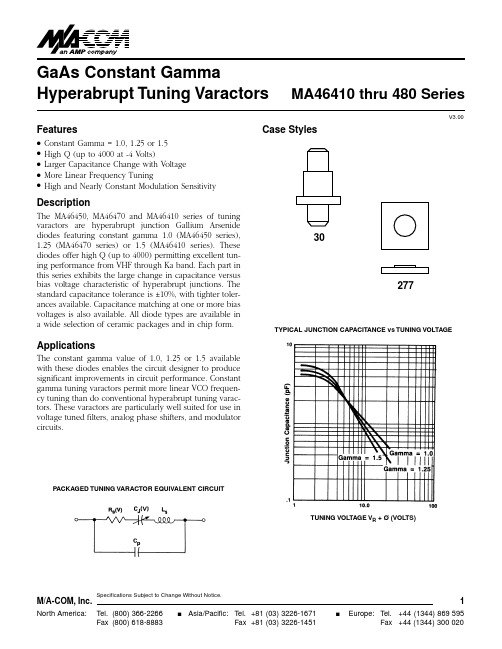
V3.00GaAs Constant GammaHyperabrupt Tuning VaractorsMA46410 thru 480 SeriesFeaturesq Constant Gamma = 1.0, 1.25 or 1.5q High Q (up to 4000 at -4 Volts)q Larger Capacitance Change with Voltage q More Linear Frequency TuningqHigh and Nearly Constant Modulation SensitivityDescriptionThe MA46450, MA46470 and MA46410 series of tuning varactors are hyperabrupt junction Gallium Arsenide diodes featuring constant gamma 1.0 (MA46450 series),1.25 (MA46470 series) or 1.5 (MA46410 series). These diodes offer high Q (up to 4000) permitting excellent tun-ing performance from VHF through Ka band. Each part in this series exhibits the large change in capacitance versus bias voltage characteristic of hyperabrupt junctions. The standard capacitance tolerance is ±10%, with tighter toler-ances available. Capacitance matching at one or more bias voltages is also available. All diode types are available in a wide selection of ceramic packages and in chip form.ApplicationsThe constant gamma value of 1.0, 1.25 or 1.5 available with these diodes enables the circuit designer to produce significant improvements in circuit performance. Constant gamma tuning varactors permit more linear VCO frequen-cy tuning than do conventional hyperabrupt tuning varac-tors. These varactors are particularly well suited for use in voltage tuned filters, analog phase shifters, and modulatorcircuits.Case Styles30277V3.00* The maximum storage and operating temperature of the plastic1088 case style is 125°C.Absolute Maximum Ratings at +25°CElectrical Specifications at 25°CMA46450 SeriesGamma = 1.0Reverse Voltage 6= 22 Volts minimum Gamma 4= 0.9 - 1.1, V R = 2 - 20 VoltsJunction Capacitance Ratio (C J2/C J20) = 5.0 - 8.0MA46470 SeriesGamma = 1.25Reverse Voltage 6= 22 Volts minimum Gamma 4= 1.13 - 1.38, V R = 2 - 20 VoltsJunction Capacitance Ratio (C J2/C J20) = 8.15 - 12.99Notes:1.All GaAs tuning varactors are available in chip form as well as the case styles shown on the following page.When ordering, specify the desired case by adding the case designation as a suffix to the type number.2.Case parasitics (C p and L s ) are given for most case styles along with case outlines in the appendix.The Cp values listed typically have toler-ances of ±0.02 pF .3.The nominal tolerance at -4 Volts is ±10%.Closer tolerances are avail-able upon request.By adding the suffix A to the part number, a toler-ance of ±5% at -4 Volts is guaranteed.4.The values guaranteed for gamma are measured on unpackaged chips.The total capacitance versus bias voltage curve will deviateslightly from the chip capacitance versus bias voltage curve due to the package parasitic capacitance (Cp).5.Capacitance is measured at 1 MHz.6.Reverse voltage (V B ) is measured at 10 microamps.7.The total capacitance and capacitance ratios shown are for diodes housed in case style 30.Other case styles will result in different val-ues.Total 2, 6, 7Total50 MHz Capacitance Capacitance 7Q at Model Case 1@ -4 Volts Ratio (2/12)-4 Volts Number Style Min./Max.(pF)Min./Max.Typical MA46410300.45-0.60 2.7-4.33000MA46413300.90-1.10 4.2-5.72500MA4641630 1.62-1.98 5.2-4.92500MA4641830 2.42-2.97 5.7-7.61800MA4642030 3.33-4.22 6.0-8.11800MA4642130 4.22-5.17 6.2-8.31200MA4642230 5.04-6.16 6.3-8.41200MA46425309.00-11.006.6-8.81200Environmental Ratings PER MIL-STD-750MIL MethodLevelStorage Temperature 1031See maximum ratingsTemperature Cycle 105110 cycles, -65°C to +175°C Shock 2016500 g’s Vibration 205615 g’s Constant Acceleration 200620,000 g’s Humidity 102110 daysMA46410 Series Gamma = 1.5Breakdown Voltage 6= 18 Volts minimum Gamma 4= 1.4 - 1.6, V R = 2 - 12 VoltsJunction Capacitance Ratio (C J2/C J12) = 6.2 - 10.84V3.00 Case Styles (See appendix for complete dimensions).1100V R(VOLTS).1100V R(VOLTS).1100V R(VOLTS).1100V R(VOLTS).1110100V R(VOLTS)V R(VOLTS).1110100V R(VOLTS)。
SN54ALS645A中文资料

PACKAGING INFORMATIONOrderable Device Status(1)PackageType PackageDrawingPins PackageQtyEco Plan(2)Lead/Ball Finish MSL Peak Temp(3)84033012A ACTIVE LCCC FK201None Call TI Level-NC-NC-NC 8403301RA ACTIVE CDIP J201None Call TI Level-NC-NC-NC 8403301SA ACTIVE CFP W201None Call TI Level-NC-NC-NC SN54ALS645AJ ACTIVE CDIP J201None Call TI Level-NC-NC-NC SN54AS645J ACTIVE CDIP J201None Call TI Level-NC-NC-NCSN74ALS645A-1DW ACTIVE SOIC DW2025Pb-Free(RoHS)CU NIPDAU Level-2-250C-1YEAR/Level-1-235C-UNLIMSN74ALS645A-1DWR ACTIVE SOIC DW202000Pb-Free(RoHS)CU NIPDAU Level-2-250C-1YEAR/Level-1-235C-UNLIMSN74ALS645A-1N ACTIVE PDIP N2020Pb-Free(RoHS)CU NIPDAU Level-NC-NC-NC SN74ALS645A-1N3OBSOLETE PDIP N20None Call TI Call TISN74ALS645A-1NSR ACTIVE SO NS202000Pb-Free(RoHS)CU NIPDAU Level-2-260C-1YEAR/Level-1-235C-UNLIMSN74ALS645ADW ACTIVE SOIC DW2025Pb-Free(RoHS)CU NIPDAU Level-2-250C-1YEAR/Level-1-235C-UNLIMSN74ALS645ADWR ACTIVE SOIC DW202000Pb-Free(RoHS)CU NIPDAU Level-2-250C-1YEAR/Level-1-235C-UNLIMSN74ALS645AN ACTIVE PDIP N2020Pb-Free(RoHS)CU NIPDAU Level-NC-NC-NC SN74ALS645AN3OBSOLETE PDIP N20None Call TI Call TISN74ALS645ANSR ACTIVE SO NS202000Pb-Free(RoHS)CU NIPDAU Level-2-260C-1YEAR/Level-1-235C-UNLIMSN74AS645DW ACTIVE SOIC DW2025Pb-Free(RoHS)CU NIPDAU Level-2-250C-1YEAR/Level-1-235C-UNLIMSN74AS645DWR ACTIVE SOIC DW202000Pb-Free(RoHS)CU NIPDAU Level-2-250C-1YEAR/Level-1-235C-UNLIMSN74AS645N ACTIVE PDIP N2020Pb-Free(RoHS)CU NIPDAU Level-NC-NC-NC SNJ54ALS645AFK ACTIVE LCCC FK201None Call TI Level-NC-NC-NC SNJ54ALS645AJ ACTIVE CDIP J201None Call TI Level-NC-NC-NC SNJ54ALS645AW ACTIVE CFP W201None Call TI Level-NC-NC-NC SNJ54AS645FK OBSOLETE LCCC FK20None Call TI Call TISNJ54AS645J ACTIVE CDIP J201None Call TI Level-NC-NC-NC SNJ54AS645W ACTIVE CFP W201None Call TI Level-NC-NC-NC (1)The marketing status values are defined as follows:ACTIVE:Product device recommended for new designs.LIFEBUY:TI has announced that the device will be discontinued,and a lifetime-buy period is in effect.NRND:Not recommended for new designs.Device is in production to support existing customers,but TI does not recommend using this part in a new design.PREVIEW:Device has been announced but is not in production.Samples may or may not be available.OBSOLETE:TI has discontinued the production of the device.(2)Eco Plan-May not be currently available-please check /productcontent for the latest availability information and additional product content details.None:Not yet available Lead(Pb-Free).Pb-Free(RoHS):TI's terms"Lead-Free"or"Pb-Free"mean semiconductor products that are compatible with the current RoHS requirements for all6substances,including the requirement that lead not exceed0.1%by weight in homogeneous materials.Where designed to be solderedat high temperatures,TI Pb-Free products are suitable for use in specified lead-free processes.Green(RoHS&no Sb/Br):TI defines"Green"to mean"Pb-Free"and in addition,uses package materials that do not contain halogens, including bromine(Br)or antimony(Sb)above0.1%of total product weight.(3)MSL,Peak Temp.--The Moisture Sensitivity Level rating according to the JEDECindustry standard classifications,and peak solder temperature.Important Information and Disclaimer:The information provided on this page represents TI's knowledge and belief as of the date that it is provided.TI bases its knowledge and belief on information provided by third parties,and makes no representation or warranty as to the accuracy of such information.Efforts are underway to better integrate information from third parties.TI has taken and continues to take reasonable steps to provide representative and accurate information but may not have conducted destructive testing or chemical analysis on incoming materials and chemicals.TI and TI suppliers consider certain information to be proprietary,and thus CAS numbers and other limited information may not be available for release.In no event shall TI's liability arising out of such information exceed the total purchase price of the TI part(s)at issue in this document sold by TI to Customer on an annual basis.IMPORTANT NOTICETexas Instruments Incorporated and its subsidiaries (TI) reserve the right to make corrections, modifications, enhancements, improvements, and other changes to its products and services at any time and to discontinue any product or service without notice. Customers should obtain the latest relevant information before placing orders and should verify that such information is current and complete. All products are sold subject to TI’s terms and conditions of sale supplied at the time of order acknowledgment.TI warrants performance of its hardware products to the specifications applicable at the time of sale in accordance with TI’s standard warranty. T esting and other quality control techniques are used to the extent TI deems necessary to support this warranty. Except where mandated by government requirements, testing of all parameters of each product is not necessarily performed.TI assumes no liability for applications assistance or customer product design. Customers are responsible for their products and applications using TI components. T o minimize the risks associated with customer products and applications, customers should provide adequate design and operating safeguards.TI does not warrant or represent that any license, either express or implied, is granted under any TI patent right, copyright, mask work right, or other TI intellectual property right relating to any combination, machine, or process in which TI products or services are used. Information published by TI regarding third-party products or services does not constitute a license from TI to use such products or services or a warranty or endorsement thereof. Use of such information may require a license from a third party under the patents or other intellectual property of the third party, or a license from TI under the patents or other intellectual property of TI.Reproduction of information in TI data books or data sheets is permissible only if reproduction is without alteration and is accompanied by all associated warranties, conditions, limitations, and notices. Reproduction of this information with alteration is an unfair and deceptive business practice. TI is not responsible or liable for such altered documentation.Resale of TI products or services with statements different from or beyond the parameters stated by TI for that product or service voids all express and any implied warranties for the associated TI product or service and is an unfair and deceptive business practice. TI is not responsible or liable for any such statements. Following are URLs where you can obtain information on other Texas Instruments products and application solutions:Products ApplicationsAmplifiers Audio /audioData Converters Automotive /automotiveDSP Broadband /broadbandInterface Digital Control /digitalcontrolLogic Military /militaryPower Mgmt Optical Networking /opticalnetwork Microcontrollers Security /securityTelephony /telephonyVideo & Imaging /videoWireless /wirelessMailing Address:Texas InstrumentsPost Office Box 655303 Dallas, Texas 75265Copyright 2005, Texas Instruments Incorporated。
变压器绝缘电阻测试标准及现场测量方法

变压器绝缘电阻测试标准及现场测量方法变压器是电力系统中重要的电气设备之一,用于改变交流电压,使之适应不同的输配电要求。
在变压器运行过程中,绝缘电阻的测量是一项必要的检测工作。
本文将详细介绍变压器绝缘电阻测试的相关标准要求以及现场测量方法。
一、变压器绝缘电阻测试标准要求变压器绝缘电阻测试主要参考国际电工委员会(IEC)标准以及国家标准。
目前国际上广泛采用的标准为IEC 60076-1《电力变压器的结构、技术特性和试验》和IEC 60076-3《电力变压器试验》。
国内标准参考了国际标准,并根据国内实际情况做出了一些调整,包括GB/T 6451《电力变压器试验规程》和DL/T596《变压器绝缘电阻和介损测试技术导则》等。
根据标准的要求,变压器绝缘电阻测试主要包括以下几个方面:1. 绝缘电阻测量的测试电压与电流范围:测试电压一般分为工频电压和直流电压。
工频电压一般为500V或1000V;直流电压一般为1000V或5000V。
测试电流一般不超过1mA。
2. 测试时间:标准一般要求绝缘电阻测试时间为1分钟,也有要求为2分钟的。
3. 测试环境条件:测试环境要求相对湿度不超过80%,温度在20℃±5℃。
4. 测试方法:绝缘电阻测试一般采用万用电表或专用绝缘电阻仪进行。
测试电源应具备足够的稳定性和准确性。
二、变压器绝缘电阻现场测量方法变压器绝缘电阻的现场测量方法需要严格按照标准要求进行,具体步骤如下:1. 准备工作:检查测试仪器的状态,确保测试仪器处于良好工作状态,如电池电量充足,测试仪器存储空间足够等。
2. 测量前的准备:断开变压器的电源,确保变压器处于安全状态。
清除表面污垢,保证测量点的干净。
3. 连接测量仪器:将测试电极连接到变压器的高压绕组与地之间,低压绕组与地之间。
注意保持电极与测量点的良好接触,以减小接触电阻。
4. 开始测量:打开测试仪器,设置测试电压和测试时间等参数。
启动测量仪器,观察并记录测量结果。
技术规格书标准模版
第五章技术规格书技术规范目录1 总则 ................................................................................................................................... 错误!未定义书签。
2 货物需求及供货范围 ....................................................................................................... 错误!未定义书签。
3 标准和规范 ....................................................................................................................... 错误!未定义书签。
4 主要技术要求 ................................................................................................................... 错误!未定义书签。
5 技术资料和交付进度 ....................................................................................................... 错误!未定义书签。
6 监造、检验/试验和性能验收试验 .................................................................................. 错误!未定义书签。
7 技术服务和设计联络 ....................................................................................................... 错误!未定义书签。
德国制造的4位数字数字显示压力传感器说明书

1:4-digit alphanumeric display 2:LEDs3:Programming buttonMade inGermanyProduct characteristics Combined pressure sensor ConnectorProcess connection:G 1A /Aseptoflex Vario Display units:bar,psi,MPa,%of the span Function programmable2-wire connection technology:analogue output3-wire connection technology:2outputsOUT1=switching outputOUT2=switching output or analogue output 4-digit alphanumeric displayMeasuring range:-1.00...10.00bar /-14.5...145.0psi /-0.100...1.000MPa Application Type of pressure:relative pressureHygienic systems,viscous media and liquids with suspended particlesLiquids and gasesApplication5MPa 725psi 50bar Pressure rating 15MPa 2175psi 150bar Bursting pressure min.5MPa725psi50barMAWP (for applications according to CRN)-25...125(145max.1h)Medium temperature [°C]Electrical data 2wires DC /3wires DC PNP/NPNElectrical design 20...32DC (2L)/18...32DC (3L)Operating voltage [V] 3.6...21(2L)/<45(3L)Current consumption [mA]>100(500V DC)Insulation resistance[MΩ]III Protection classyesReverse polarity protection Outputs 2-wire connection technology:analogue output3-wire connection technology:2outputsOUT1=switching outputOUT2=switching output or analogue outputOutput1x normally open /normally closed programmable +1x normally open /normallyclosed programmable or 1x analogue (4...20/20...4mA,scalable)Output function ---(2L)/250(3L)Current rating [mA]---(2L)/<2(3L)Voltage drop[V]pulsed Short-circuit protection yesOverload protection ---(2L)/125(3L)Switching frequency [Hz]I:4...20mA (Ineg:20...4mA)Analogue output 300(2L)/max.(Ub -10V)x 50(3L)Max.load[Ω]Measuring /setting range -0.100...1.000MPa -14.5...145.0psi -1.00...10.00bar Measuring range Setting range -0.098...1.000MPa -14.2...145.0psi -0.98...10.00bar Set point,SP -0.100...0.998MPa -14.5...144.7psi -1.00...9.98bar Reset point,rP-0.100...0.750MPa -14.5...108.7psi -1.00...7.50bar Analogue start point,ASP 0.150...1.000MPa21.8...145.0psi1.50...10.00barAnalogue end point,AEP 0.001MPa0.1psi0.01barin steps of SP1=2.50bar;rP1=2.30bar SP2=7.50bar;rP2=7.30bar ASP =0.00bar;AEP =10.00barFactory settingAccuracy /deviations Accuracy /deviations(in %of the span)Turn down 1:1<±0.2Switch point accuracy <±0.2Characteristics deviation *)<±0.15Linearity <±0.15Hysteresis <±0.1Repeatability **)<±0.1Long-term stability ***)Temperature coefficients (TEMPCO)in the temperature range 0...70°C (in %of the span per 10K)<±0.05Greatest TEMPCO of the zero point <±0.15Greatest TEMPCO of the span Reaction times 1(2L)/0.5(3L)Power-on delay time [s]---(2L)/3(3L)Min.response time switching output[ms]0.00...30.00Damping for the switching output (dAP)[s]0.01...99.99Damping for the analogue output (dAA)[s]45(2L)/7(3L)Step response time analogue output[ms]yesIntegrated watchdog Interfaces IO-Link Device COM2(38.4kBaud)Transfer type 1.0IO-Link revision 157d /00009D hIO-Link Device ID no profile Profiles yes SIO modeA Required master port type 1Process data analogue 2Process data binary 2.3Min.process cycle time [ms]Environment -25...80Ambient temperature [°C]-40...100Storage temperature [°C]IP 67/IP 68/IP 69KProtection Tests /approvals EMCDIN EN 61000-6-2DIN EN 61000-6-3Shock resistance 50g (11ms)DIN EN 60068-2-27:Vibration resistance 20g (10...2000Hz)DIN EN 60068-2-6:160MTTF[Years]Mechanical data G 1A /Aseptoflex VarioProcess connection ceramics (99.9%Al2O3);PTFE;stainless steel 316L /1.4435;surfacecharacteristics:Ra <0.4/Rz 4Materials (wetted parts)stainless steel 316L /1.4404;FPM;PTFE;PBT;PEI;PFAHousing materials 100million Switching cycles min.0.313Weight[kg]Displays /operating elements DisplayLED green Display unit LED yellowSwitching status 4-digit alphanumeric display Function display 4-digit alphanumeric displayMeasured values Electrical connection M12connector;Gold-plated contactsConnection Wiring1connection for2-wire operation2connection for3-wire operation3connection for IO-Link parameter setting(P=communication via IO-Link)RemarksRemarks(2L)=value for2-wire operation(3L)=value for3-wire operation*)linearity,incl.hysteresis and repeatability;(limit value setting to DIN16086)**)with temperature fluctuations<10K***)in%of the span per year1Pack quantity[piece]ifm electronic gmbh•Friedrichstraße1•45128Essen—We reserve the right to make technical alterations without prior notice.—GB—PI2794—16.04.2013。
电子课件-《维修电工技能训练(第四版)》-A04-6451 第七单元
2U 2
二、单相桥式整流、滤波电路的安装与调试
1. 电路的安装 配齐元器件→清除元件氧化层并搪锡→连接线搪锡→ 插装元器件→焊接元器件→清扫现场 组装好的电路板及其焊接面如图所示。
单相桥式整流滤波电路板
单相桥式整流滤波电路的焊接面
2.测试
安装电源→检查各元器件的焊接质量→通电测试 (1)在胶木板上安装变压器、开关、熔断器等元器件。 同时,要求做好电源引线的连接和电路板交流输入端的连 接。 (2)检查各元器件有无错焊、漏焊和虚焊等情况,并判 断接线是否正确。 (3)接通电源,观察有无异常情况,在开关S1和S2处于 各种状态时,将万用表的量程转换开关置于直流50V挡,用 万用表测量输出电压的平均值。测量时,红表笔接输出端 正极,黑表笔接输出端负极,空载输出电压应为18V左右。
课题三 印制电路制作工艺
一、印制电路板的制作工艺 二、电子元器件的安装
一、印制电路板的制作工艺
1.印制电路板设计前的准备
(1)板材的准备 印制电路板一般采用覆铜板制作。所 谓覆铜板就是把一定厚度的铜箔通过黏接剂热压在一定厚 度的绝缘基板上。
(2)印制板对外连接方法的选择 1)引线焊接方法 导线焊接方法应注再从线路板元件面穿过,焊在焊盘上,多根引线 应捆扎。 2)插件连接 在较复杂的仪器设备中,经常采用这种方 式。
(2)元器件的安装与布局 1)安装方式 元器件在印制板上的固定方式分为卧式和 立式两种。 2)元器件排列格式 它分为不规则排列和规则排列两种。 前者元件轴线方向彼此不一致,在板上的排列顺序也无一定 规则;但布线方便,印制导线短,对抑制干扰有利。后者元 器件轴线方向一致,并与板四边平行;但布线复杂,一般用 于低频电路中。 3)元器件布设原则 元器件在整个版面疏密应一致,布设 均匀,不要占满版面,四周留空便于安装固定。元器件布设 在板的一面,每个引脚单独占用一个焊盘。在布设时不可上 下交叉,相邻元器件要保持一定距离,并留有安全间隙 (200V/mm)。安装高度尽量矮一些,以提高稳定性和防止 相邻元器件碰撞。同时要根据在整流中安装状态确定元件轴 向位置,以提高元器件在板上的稳定性。
MAX4544ESA+中文资料

For pricing, delivery, and ordering information,please contact Maxim Direct at 1-888-629-4642,or visit Maxim’s website at .General DescriptionThe MAX4541–MAX4544 are precision, dual analog switches designed to operate from a single +2.7V to +12V supply. Low power consumption (5µW) makes these parts ideal for battery-powered equipment. These switches offer low leakage currents (100pA max) and fast switching speeds (t ON = 150ns max, t OFF = 100ns max).When powered from a +5V supply, the MAX4541–MAX4544 offer 2Ωmax matching between channels, 60Ωmax on-resistance (R ON ), and 6Ωmax R ON flatness.These switches also offer 5pC max charge injection and a minimum of 2000V ESD protection per Method 3015.7.The MAX4541/MAX4542/MAX4543 are dual single-pole/single-throw (SPST) devices and the MAX4544 is a single-pole/double-throw (SPDT) device. The MAX4541 has two normally open (NO) switches and the MAX4542 has two normally closed (NC) switches. The MAX4543 has one NO and one NC switch and can be used as an SPDT, while the MAX4544 is an SPDT. The MAX4541/MAX4542/MAX4543are available in tiny SOT23-8 and 8-pin TDFN packages,and the MAX4544 is available in a SOT23-6 package.________________________Applications____________________________Features♦60Ωmax (33Ωtyp) Low R ON♦2Ωmax R ON Matching Between Channels ♦6Ωmax R ON Flatness♦5pC max Guaranteed Charge Injection ♦+2.7V to +12V Single-Supply Operation ♦< 5µW Low Power Consumption♦Low Leakage Current Over Temperature: 10nA max at +85°C♦Fast Switching: t ON = 35ns, t OFF = 25ns ♦Guaranteed Break-Before-Make (MAX4543/MAX4544 Only)♦TTL/CMOS-Logic Compatible♦Pin Compatible with MAX323/MAX324/MAX325♦MAX4541/MAX4542/MAX4543 Available in SOT23-8MAX4544 Available in SOT23-6MAX4541–MAX4544Low-Voltage, Single-SupplyDual SPST/SPDT Analog Switches________________________________________________________________Maxim Integrated Products 119-1202; Rev 4; 6/07Ordering Information continued at end of data sheet.*Dice are specified at T A = +25°C.**EP = Exposed pad.Pin Configurations/Functional Diagrams/Truth TablesBattery-Operated Systems Sample-and-Hold Circuits Heads-Up Displays Guidance and Control SystemsAudio and Video SwitchingMilitary RadiosTest EquipmentCommunications Systems +3V/+5V DACs and ADCs PBX, PABX Cell Phones Ultrasound PagersµMAX is a registered trademark of Maxim Integrated Products, Inc.M A X 4541–M A X 4544Low-Voltage, Single-SupplyDual SPST/SPDT Analog Switches 2_______________________________________________________________________________________Voltage Referenced to GNDV+.........................................................................-0.3V to +13V IN_, COM_, NC_, NO_ (Note 1)..................-0.3V to (V+ + 0.3V)Continuous Current (any terminal)....................................±10mA Peak Current, COM_, NO_, NC_(pulsed at 1ms, 10% duty cycle max)............................±20mA ESD per Method 3015.7.................................................> 2000V Continuous Power DissipationSOT23-6 (derate 7.1mW/°C above +70°C)....................571mW SOT23-8 (derate 5.3mW/°C above +70°C)....................421mWTDFN (derate 24.4mW/°C above +70°C).....................1951mW µMAX (derate 4.10mW/°C above +70°C)......................330mW Narrow SO (derate 5.88mW/°C above +70°C)..............471mW Plastic DIP (derate 9.09mW/°C above +70°C)..............727mW Operating Temperature RangesMAX454_C_ _.......................................................0°C to +70°C MAX454_E_ _.....................................................-40°C to +85°C Storage Temperature Range.............................-65°C to +150°C Lead Temperature (soldering, 10s).................................+300°CStresses beyond those listed under “Absolute Maximum Ratings” may cause permanent damage to the device. These are stress ratings only, and functional operation of the device at these or any other conditions beyond those indicated in the operational sections of the specifications is not implied. Exposure to absolute maximum rating conditions for extended periods may affect device reliability.ABSOLUTE MAXIMUM RATINGSELECTRICAL CHARACTERISTICS—Single +5V Supply(V+ = +5V ±10%, GND = 0, V INH = 2.4V, V INL = 0.8V, T A = T MIN to T MAX , unless otherwise noted.) (Notes 2, 3)Note 1:Signals on NC_, NO_, COM_, or IN_ exceeding V+ or V- are clamped by internal diodes. Limit forward diode current to maximumcurrent rating.MAX4541–MAX4544Low-Voltage, Single-SupplyDual SPST/SPDT Analog Switches_______________________________________________________________________________________3ELECTRICAL CHARACTERISTICS—Single +5V Supply (continued)(V+ = +5V ±10%, GND = 0, V INH = 2.4V, V INL = 0.8V, T A = T MIN to T MAX , unless otherwise noted.) (Notes 2, 3)M A X 4541–M A X 4544Low-Voltage, Single-SupplyDual SPST/SPDT Analog Switches 4_______________________________________________________________________________________ELECTRICAL CHARACTERISTICS—Single +3.3V Supply(V+ = +3.0V to +3.6V, GND = 0, V INH = 2.4V, V INL = 0.8V, T A = T MIN to T MAX , unless otherwise noted.) (Notes 2, 3)Note 2:QFN and SOT-packaged parts are 100% tested at +25°C only and guaranteed by correlation at the full hot rated temperature.Note 3:The algebraic convention, where the most negative value is a minimum and the most positive value a maximum, is used inthis data sheet.Note 4:Guaranteed by design.Note 5:ΔR ON = ΔR ON max - ΔR ON min.Note 6:Flatness is defined as the difference between the maximum and minimum value of on-resistance as measured over thespecified analog signal range.Note 7:Leakage parameters are 100% tested at maximum rated hot temperature and guaranteed by correlation at +25°C.Note 8:Off-isolation = 20 x log 10[V COM ⁄ (V NC or V NO )], V COM = output, V NC or V NO = input to off switch.Note 9:Between the two switches, MAX4541/MAX4542/MAX4543 only.MAX4541–MAX4544Low-Voltage, Single-SupplyDual SPST/SPDT Analog Switches_______________________________________________________________________________________51020304050607080024681012ON-RESISTANCE vs. COM_ VOLTAGEV COM_ (V)R O N (Ω)102030405060012345ON-RESISTANCE vs.COM VOLTAGE OVER TEMPERATUREV COM (V)R O N (Ω)2040608010012014016018020024681012TURN-ON/OFF TIMES vs.SUPPLY VOLTAGEV SUPPLY (V)t O N /t O F F (n s )102030405060708090100TURN-ON/OFF TIMES vs. TEMPERATURETEMPERATURE (°C)t O N /t O F F (n s )-55-35-15525456585105125-100-90-80-70-60-50-40-30-20-1000.1110100FREQUENCY RESPONSEFREQUENCY (MHz)L O S S (d B )-225-180-135-90-4504590135180225P H A S E (D E G R E E S )0.0010.010.1110100ON/OFF-LEAKAGE CURRENTvs. TEMPERATURETEMPERATURE (°C)O N /O F F -L E A K A G E (n A )-55-30-5204570951201251234567812345CHARGE INJECTION vs. COM_ VOLTAGEV COM_ (V)Q (p C )1002003004005006007008009001000INPUT VOLTAGE vs. SUPPLY CURRENTM A X 4541-08VIN (V)I + (n A )12345I V+100.111001k 10kTOTAL HARMONIC DISTORTIONvs. FREQUENCYFREQUENCY (Hz)T H D (%)__________________________________________Typical Operating Characteristics(T A = +25°C, unless otherwise noted.)M A X 4541–M A X 4544Low-Voltage, Single-SupplyDual SPST/SPDT Analog Switches 6_______________________________________________________________________________________Applications InformationLogic LevelsThe MAX4541–MAX4544 are TTL compatible whenpowered from a single +5V supply. When powered from other supply voltages, TTL compatibility is guar-anteed and the logic inputs can be driven rail-to-rail.For example, with a +12V supply, IN1 and IN2 can be driven low to 0 and high to 12V. With a +3.3V supply,IN1 and IN2 should be driven low to 0 and high to 3.3V.Driving IN1 and IN2 rail-to-rail minimizes power con-sumption.Analog Signal LevelsAnalog signals that range over the entire supply voltage (V+ to GND) can be switched with very little change in on-resistance over the entire voltage range (see the Typical Operating Characteristics ). All the switches are bidirectional, so the NO_, NC_, and COM_ pins can be used as either inputs or outputs.Pin DescriptionFigure 1. Overvoltage Protection Using Two External Blocking DiodesPower-Supply Sequencing and Overvoltage ProtectionDo not exceed the absolute maximum ratings because stresses beyond the listed ratings may cause perma-nent damage to the devices.Proper power-supply sequencing is recommended for all CMOS devices. Always apply V+ before applying analog signals or logic inputs, especially if the analog or logic signals are not current limited. If this sequenc-ing is not possible, and if the analog or logic inputs are not current limited to <10mA, add a small-signal diode (D1) as shown in Figure 1. If the analog signal can dip below GND, add D2. Adding protection diodes reduces the analog signal range to a diode drop (about 0.7V) below V+ (for D1), and to a diode drop above ground (for D2). Leakage is unaffected by adding the diodes. On-resistance increases by a small amount at low supply voltages. Maximum supply voltage (V+)must not exceed 13V.Adding protection diodes causes the logic thresholds to be shifted relative to the power-supply rails. This can be significant when low supply voltages (+5V or less)are used. With a +5V supply, TTL compatibility is not guaranteed when protection diodes are added. Driving IN1 and IN2 all the way to the supply rails (i.e., to a diode drop higher than the V+ pin, or to a diode drop lower than the GND pin) is always acceptable.Protection diodes D1 and D2 also protect against some overvoltage situations. With Figure 1’s circuit, if the supply voltage is below the absolute maximum rat-ing, and if a fault voltage up to the absolute maximum rating is applied to an analog signal pin, no damage will result.MAX4541–MAX4544Low-Voltage, Single-SupplyDual SPST/SPDT Analog Switches_______________________________________________________________________________________7Figure 2. Switching TimeTest Circuits/Timing DiagramsM A X 4541–M A X 4544Low-Voltage, Single-SupplyDual SPST/SPDT Analog Switches 8_______________________________________________________________________________________Figure 4. Charge InjectionFigure 3a. Break-Before-Make Interval (MAX4543 Only)Figure 3b. Break-Before-Make Interval (MAX4544 Only)_________________________________Test Circuits/Timing Diagrams (continued)MAX4541–MAX4544Low-Voltage, Single-SupplyDual SPST/SPDT Analog Switches_______________________________________________________________________________________9Figure 6. CrosstalkFigure 5. Off-Isolation _________________________________Test Circuits/Timing Diagrams (continued)Figure 7. Channel Off/On-CapacitanceM A X 4541–M A X 4544Low-Voltage, Single-SupplyDual SPST/SPDT Analog Switches 10_________________________________________________________________________________________Ordering Information (continued)*Dice are specified at T A = +25°C.**EP = Exposed pad.MAX4541–MAX4544Dual SPST/SPDT Analog Switches______________________________________________________________________________________11_________Pin Configurations/Functional Diagrams/Truth Tables (continued)M A X 4541–M A X 4544Dual SPST/SPDT Analog Switches 12Package Information(The package drawing(s) in this data sheet may not reflect the most current specifications. For the latest package outline information go to /packages .)MAX4541–MAX4544Dual SPST/SPDT Analog Switches______________________________________________________________________________________13Package Information (continued)(The package drawing(s) in this data sheet may not reflect the most current specifications. For the latest package outline information go to /packages .)M A X 4541–M A X 4544Dual SPST/SPDT Analog Switches 14______________________________________________________________________________________Package Information (continued)(The package drawing(s) in this data sheet may not reflect the most current specifications. For the latest package outline information go to /packages .)MAX4541–MAX4544______________________________________________________________________________________15S O T 23, 8L .E P SPackage Information (continued)(The package drawing(s) in this data sheet may not reflect the most current specifications. For the latest package outline information go to /packages .)Revision HistoryPages changed at Rev 4: 1–16M A X 4541–M A X 4544Dual SPST/SPDT Analog Switches Maxim cannot assume responsibility for use of any circuitry other than circuitry entirely embodied in a Maxim product. No circuit patent licenses are implied. Maxim reserves the right to change the circuitry and specifications without notice at any time.16____________________Maxim Integrated Products, 120 San Gabriel Drive, Sunnyvale, CA 94086 408-737-7600©2007 Maxim Integrated Productsis a registered trademark of Maxim Integrated Products, Inc.。
MAR-4SM中文资料

Distribution Centers/ NORTH AMERICA 800-654-7949 ¨ 417-335-5935 Fax 417-335-5945 EUROPE 44-1252-835094 Fax 44-1252-837010
961111
MONOLITHIC AMPLIFIERS 50 Ω
BROADBAND DC to 2.5 GHz
MAR-SM
MAV-SM
up to +18 dBm output
MODEL NO.
MAR-1SM MAR-2SM MAR-3SM MAR-4SM
MAR-6SM MAR-7SM MAR-8SM
JFREQ. MHz
marking identification
Alphanumeric
Color
Model
Code OR Dot
MAR-1SM MAR-2SM MAR-3SM MAR-4SM MAR-6SM MAR-7SM MAR-8SM
A01
Brown
A02
Red
A03
Orange
A04
Yellow
A06
White
10
1 100
120
140
160
180
Junction Temperature (°C)
200
1 140
150
160
170
180
190
200
JUNCTION TEMPERATURE (°C)
3-6 108
®
INTERNET
P.O. Box 350166, Brooklyn, New York 11235-0003 (718) 934-4500 Fax (718) 332-4661
- 1、下载文档前请自行甄别文档内容的完整性,平台不提供额外的编辑、内容补充、找答案等附加服务。
- 2、"仅部分预览"的文档,不可在线预览部分如存在完整性等问题,可反馈申请退款(可完整预览的文档不适用该条件!)。
- 3、如文档侵犯您的权益,请联系客服反馈,我们会尽快为您处理(人工客服工作时间:9:00-18:30)。
V3.00
GaAs Constant Gamma
Hyperabrupt Tuning Varactors
MA46410 thru 480 Series
Features
q Constant Gamma = 1.0, 1.25 or 1.5q High Q (up to 4000 at -4 Volts)
q Larger Capacitance Change with Voltage q More Linear Frequency Tuning
q
High and Nearly Constant Modulation Sensitivity
Description
The MA46450, MA46470 and MA46410 series of tuning varactors are hyperabrupt junction Gallium Arsenide diodes featuring constant gamma 1.0 (MA46450 series),1.25 (MA46470 series) or 1.5 (MA46410 series). These diodes offer high Q (up to 4000) permitting excellent tun-ing performance from VHF through Ka band. Each part in this series exhibits the large change in capacitance versus bias voltage characteristic of hyperabrupt junctions. The standard capacitance tolerance is ±10%, with tighter toler-ances available. Capacitance matching at one or more bias voltages is also available. All diode types are available in a wide selection of ceramic packages and in chip form.
Applications
The constant gamma value of 1.0, 1.25 or 1.5 available with these diodes enables the circuit designer to produce significant improvements in circuit performance. Constant gamma tuning varactors permit more linear VCO frequen-cy tuning than do conventional hyperabrupt tuning varac-tors. These varactors are particularly well suited for use in voltage tuned filters, analog phase shifters, and modulator
circuits.
Case Styles
30
277
V3.00
* The maximum storage and operating temperature of the plastic
1088 case style is 125°C.
Absolute Maximum Ratings at +25°C
Electrical Specifications at 25°C
MA46450 Series
Gamma = 1.0
Reverse Voltage 6= 22 Volts minimum Gamma 4= 0.9 - 1.1, V R = 2 - 20 Volts
Junction Capacitance Ratio (C J2/C J20) = 5.0 - 8.0
MA46470 Series
Gamma = 1.25
Reverse Voltage 6= 22 Volts minimum Gamma 4= 1.13 - 1.38, V R = 2 - 20 Volts
Junction Capacitance Ratio (C J2/C J20) = 8.15 - 12.99
Notes:
1.All GaAs tuning varactors are available in chip form as well as the case styles shown on the following page.When ordering, specify the desired case by adding the case designation as a suffix to the type number.
2.Case parasitics (C p and L s ) are given for most case styles along with case outlines in the appendix.The Cp values listed typically have toler-ances of ±0.02 pF .
3.The nominal tolerance at -4 Volts is ±10%.Closer tolerances are avail-able upon request.By adding the suffix A to the part number, a toler-ance of ±5% at -4 Volts is guaranteed.
4.The values guaranteed for gamma are measured on unpackaged chips.The total capacitance versus bias voltage curve will deviate
slightly from the chip capacitance versus bias voltage curve due to the package parasitic capacitance (Cp).5.Capacitance is measured at 1 MHz.
6.Reverse voltage (V B ) is measured at 10 microamps.
7.The total capacitance and capacitance ratios shown are for diodes housed in case style 30.Other case styles will result in different val-ues.
Total 2, 6, 7Total
50 MHz Capacitance Capacitance 7Q at Model Case 1@ -4 Volts Ratio (2/12)-4 Volts Number Style Min./Max.(pF)Min./Max.
Typical MA46410300.45-0.60 2.7-4.33000MA46413300.90-1.10 4.2-5.72500MA4641630 1.62-1.98 5.2-4.92500MA4641830 2.42-2.97 5.7-7.61800MA4642030 3.33-4.22 6.0-8.11800MA4642130 4.22-5.17 6.2-8.31200MA4642230 5.04-6.16 6.3-8.41200MA46425
30
9.00-11.00
6.6-8.8
1200
Environmental Ratings PER MIL-STD-750
MIL Method
Level
Storage Temperature 1031See maximum ratings
Temperature Cycle 105110 cycles, -65°C to +175°C Shock 2016500 g’s Vibration 205615 g’s Constant Acceleration 200620,000 g’s Humidity 1021
10 days
MA46410 Series Gamma = 1.5
Breakdown Voltage 6= 18 Volts minimum Gamma 4= 1.4 - 1.6, V R = 2 - 12 Volts
Junction Capacitance Ratio (C J2/C J12) = 6.2 - 10.84
V3.00 Case Styles (See appendix for complete dimensions)
.1100
V R(VOLTS).1100
V R(VOLTS)
.1100
V R(VOLTS)
.1100
V R(VOLTS)
.1110100
V R(VOLTS)
V R(VOLTS).1110100
V R(VOLTS)。