7070T中文资料
HT7070A中文资料

HT70XXVoltage DetectorSelection TablePart No.Detectable VoltageHysteresis WidthTolerance HT7022A 2.2V 0.11V ±5%HT7024A 2.4V 0.12V ±5%HT7027A 2.7V 0.135V ±5%HT7033A 3.3V 0.165V ±5%HT7039A 3.9V 0.195V ±5%HT7044A 4.4V 0.22V ±5%HT7050A 5.0V 0.25V ±5%HT7070A 7.0V0.35V±5%Note:The output type selection codes are:NMOS open drain normal open,active lowFor example:The HT7070A is a 7.0V,NMOS open drain active low outputOutput type selection tableV DDV DD >V DET (+)V DD £V DET (-)TypeV OUT AHi-ZVSSRev.1.601January 14,2003General DescriptionThe HT70XX series is a set of three-terminal low power voltage detectors implemented in CMOS technology.Each voltage detector in the series detects a particular fixed voltage ranging from 2.2V to 7V.The voltage de-tectors consist of a high-precision and low power con-sumption standard voltage source,a comparator,hysteresis circuit,and an output driver.CMOS technol-ogy ensures low power consumption.Although designed primarily as fixed voltage detectors,these devices can be used with external components to detect user specified threshold voltages (NMOS open drain type only).Features·Low power consumption ·Low temperature coefficient·Built-in high-stability reference source·Built-in hysteresis characteristic ·TO-92&SOT-89packageApplications·Battery checkers ·Level selectors ·Power failure detectors·Microcomputer reset ·Battery memory backup·Non-volatile RAM signal storage protectorsBlock DiagramN channel open drain output(normal open;active low)A typePin AssignmentRev.1.602January14,2003Pad AssignmentHT70XX (except HT7022A)Chip size:1317´1158(m m)2*The IC substrate should be connected to VDD in the PCB layout artwork.HT7022A onlyChip size:2032´1321(m m)2*The IC substrate should be connected to VDD in the PCB layout artwork.Absolute Maximum RatingsSupply Voltage,except HT7022A..................................................................................................V SS -0.3V to V SS +26V Supply Voltage,HT7022A only....................................................................................................................-0.3V to13V Output Voltage...........................V SS -0.3V to V DD +0.3V Output Current......................................................50mA Storage Temperature............................-50°C to 125°C Power Consumption..........................................200mWOperating Temperature 0°C to 70°CNote:These are stress ratings only.Stresses exceeding the range specified under ²Absolute Maximum Ratings ²maycause substantial damage to the device.Functional operation of this device at other conditions beyond those listed in the specification is not implied and prolonged exposure to extreme conditions may affect device reliabil-ity.Rev.1.603January 14,2003Pad CoordinatesHT70XX (except HT7022A)Unit:m m Pad No.X Y 1-483.30-379.502-234.60-399.503443.90-386.00HT7022A onlyUnit:m mPad No.X Y1-434.34394.972120.65461.013774.70412.75Electrical CharacteristicsHT7022A Ta=25°CHT7024A Ta=25°CHT7027A Ta=25°CRev.1.604January14,2003HT7039A Ta=25°CHT7044A Ta=25°CRev.1.605January14,2003HT7070A Ta=25°CRev.1.606January 14,2003Functional DescriptionThe HT70XX series is a set of voltage detectors equipped with a high stability voltage reference which is connected to the negative input of a comparator ¾de-noted as V REF in the following figure for NMOS output voltage detector.When the voltage drop to the positive input of the com-parator (i,e,V B )is higher than V REF ,VOUT goes high,M1turns off,and V B is expressed as V BH =V DD ´(R B +R C )/(R A +R B +R C ).If V DD is decreased so that V B falls to a value less than V REF ,the comparator output in-verts from high to low,V OUT goes low,V C is high,M1turns on,RC is bypassed,and V B becomes:V BL =V DD ´R B /(R A +R B ),which is less than V BH.By so doing,the comparator output will stay low to prevent the circuit from oscillating when V B »V REF.If V DD falls below the minimum operating voltage,the output becomes undefined.When VDD goes from low to V DD ´R B /(R A +R B )>V REF ,the comparator output and V OUT goes high.The detectable voltage is defined as:V DET (-)=R R R R R A B CB C +++´V REFThe release voltage is defined as:V DET (+)=R R R A BB+´V REFThe hysteresis width is:V HYS=V DET(+)-V DET(-)The figure demonstrates the NMOS output type withpositive output polarity(V OUT is normally open,activelow).The HT70XX series also supplies options for otheroutput types with active high outputs.Application cir-cuits shown are examples of positive output polarity(normally open,active low)unless otherwise specified.NMOS output voltage detector(HT70XXA) Application CircuitsMicrocomputer reset circuitNormally a reset circuit is required to protect the micro-computer system from malfunctions due to power line interruptions.The following examples show how differ-ent output configurations perform a reset function in var-ious systems.·NMOS open drain output application for separate power supply·NMOS open drain output application with R-C delayPower-on reset circuitWith several external components,the NMOS open drain type of the HT70XX series can be used to perform a power-on reset function as shown:Rev.1.607January14,20035V power line monitoring circuitGenerally,a minimum operating voltage of4.5V is guar-anteed in a5V power line system.The HT7044A is rec-ommended for use as5V power line monitoring circuit.·5V power line monitor with power-on reset·with5V voltage regulatorChange of detectable voltageIf the required voltage is not found in the standard prod-uct selection table,it is possible to change it by using ex-ternal resistance dividers or diodes.·Varying the detectable voltage with a resistance di-viderDetectable voltage=R RRA BB+´V DETHysteresis width=R RRA BB+´V HYS·Varying the detectable voltage with a diodeDetectable Voltage=V f1+V f2+V DETMalfunction analysisThe following circuit demonstrates the way a circuit ana-lyzes malfunctions by monitoring the variation or spikenoise of power supply voltage.Charge monitoring circuitThe following circuit shows a charged monitor for pro-tection against battery deterioration by overcharging.When the voltage of the battery is higher than the set de-tectable voltage,the transistor turns on to bypass thecharge current,protecting the battery from overcharg-ing.Rev.1.608January14,2003Level selectorThe following diagram illustrates a logic level selector.Rev.1.609January14,2003Package Information3-pin TO-92outline dimensionsSymbolDimensions in milMin.Nom.Max.A170¾200B170¾200C500¾¾D11¾20E90¾110F45¾55G45¾65H130¾160I8¾18a4°¾6°Rev.1.6010January14,20033-pin SOT-89outline dimensionsSymbolDimensions in milMin.Nom.Max.A173¾181B64¾72C90¾102D35¾47E155¾167F14¾19G17¾22H¾59¾I55¾63J14¾17Rev.1.6011January14,2003Product Tape and Reel SpecificationsTO-92reel dimensions(Unit:mm)Rev.1.6012January14,2003SOT-89reel dimensionsSOT-89Symbol Description Dimensions in mmA Reel Outer Diameter180±1.0B Reel Inner Diameter62±1.5C Spindle Hole Diameter12.75+0.15D Key Slit Width 1.9±0.15T1Space Between Flange12.4+0.2T2Reel Thickness17-0.4Rev.1.6013January14,2003TO-92Symbol Description Dimensions in mm I1Taped Lead Length(2.5)P Component Pitch12.7±1.0P0Perforation Pitch12.7±0.3P2Component to Perforation(Length Direction) 6.35±0.4F1Lead Spread 2.5+0.4-0.1F2Lead Spread 2.5+0.4-0.1D h Component Alignment0±0.1W Carrier Tape Width 18.0+1.0-0.5W0Hold-down Tape Width 6.0±0.5W1Perforation Position9.0±0.5W2Hold-down Tape Position(0.5)H0Lead Clinch Height16.0±0.5H1Component Height Less than24.7D0Perforation Diameter 4.0±0.2t Taped Lead Thickness0.7±0.2H Component Base Height19.0±0.5Note:Thickness less than0.38±0.05mm~0.5mmP0Accumulated pitch tolerance:±1mm/20pitches.()Bracketed figures are for consultation onlyRev.1.6014January14,2003SOT-89Symbol Description Dimensions in mmW Carrier Tape Width 12.0+0.3-0.1P Cavity Pitch8.0±0.1E Perforation Position 1.75±0.1F Cavity to Perforation(Width Direction) 5.5±0.05D Perforation Diameter 1.5+0.1D1Cavity Hole Diameter 1.5+0.1P0Perforation Pitch 4.0±0.1P1Cavity to Perforation(Length Direction) 2.0±0.10A0Cavity Length 4.8±0.1B0Cavity Width 4.5±0.1K0Cavity Depth 1.8±0.1t Carrier Tape Thickness0.30±0.013C Cover Tape Width9.3Rev.1.6015January14,2003Holtek Semiconductor Inc.(Headquarters)No.3,Creation Rd.II,Science-based Industrial Park,Hsinchu,TaiwanTel:886-3-563-1999Fax:886-3-563-1189Holtek Semiconductor Inc.(Sales Office)11F,No.576,Sec.7Chung Hsiao E.Rd.,Taipei,TaiwanTel:886-2-2782-9635Fax:886-2-2782-9636Fax:886-2-2782-7128(International sales hotline)Holtek Semiconductor(Shanghai)Inc.7th Floor,Building2,No.889,Yi Shan Rd.,Shanghai,ChinaTel:021-6485-5560Fax:021-6485-0313Holtek Semiconductor(Hong Kong)Ltd.RM.711,Tower2,Cheung Sha Wan Plaza,833Cheung Sha Wan Rd.,Kowloon,Hong KongTel:852-2-745-8288Fax:852-2-742-8657Holmate Semiconductor,Inc.48531Warm Springs Boulevard,Suite413,Fremont,CA94539Tel:510-252-9880Fax:510-252-9885CopyrightÓ2003by HOLTEK SEMICONDUCTOR INC.The information appearing in this Data Sheet is believed to be accurate at the time of publication.However,Holtek as-sumes no responsibility arising from the use of the specifications described.The applications mentioned herein are used solely for the purpose of illustration and Holtek makes no warranty or representation that such applications will be suitable without further modification,nor recommends the use of its products for application that may present a risk to human life due to malfunction or otherwise.Holtek reserves the right to alter its products without prior notification.For the most up-to-date information,please visit our web site at .Rev.1.6016January14,2003。
WP710A10NT;中文规格书,Datasheet资料

Notes: 1. θ1/2 is the angle from optical centerline where the luminous intensity is 1/2 of the optical peak value. 2. Luminous intensity/ luminous Flux: +/-15%.
PACKING & LABEL SPECIFICATIONS
WP710A10NT
SPEC NO: DSAL0516 APPROVED: WYNEC
REV NO: V.2 CHECKED: Allen Liu
DATE: MAR/07/2011 DRAWN: J.Yu
PAGE: 4 OF 6 ERP: 1101029070
Notes: 1. 1/10 Duty Cycle, 0.1ms Pulse Width. 2. 2mm below package base. 3. 5mm below package base.
Pure Orange 62.5 25 145 5 -40°C To +85°C 260°C For 3 Seconds 260°C For 5 Seconds
/
SPEC NO: DSAL0516 APPROVED: WYNEC
REV NO: V.2 CHECKED: Allen Liu
DATE: MAR/07/2011 DRAWN: J.Yu
福建天电光电EMC7070系列LED器件使用指南说明书
导言尊敬的客户:感谢您使用福建天电光电有限公司生产的LED产品,为使您更好地了解我司产品的特性,方便您快速掌握我司产品的基本操作,特编写此册使用指南。
指南中的说明及注意事项,将帮助您安全、规范、合理的使用本公司的产品,避免或减少因不当的使用而造成产品损伤,进而影响到产品性能。
我们编写本指南的目的,就是使其能更好的为您提供服务,同时,我们还会根据您的需要提供完善的技术支持及售前、售后服务。
本册指南所述仅为我司产品的一部分,在您使用我司LED产品前,请您务必仔细阅读本使用指南,结合我司最新版的产品规格书,全面了解所选用的LED器件的使用条件,使用手法及相关的极限参数,对可能存在隐患的作业手法、使用条件等进行相应的规避处理,并在产品的可使用期内妥善保存。
同时需要说明的是,即使同一规格的产品,在实际应用领域其可靠性与整体的系统设计方案、作业方法、工作条件、环境因素等息息相关,使用指南中的内容无法涵盖您使用过程中可能涉及到的所有问题,而部分内容虽然有涵盖,但可能没有提供详细的说明,由此带来的不便,敬请谅解!为此,我们将根据您在实际使用过程中的典型案例和相关信息反馈,不定期更新本使用指南,期间如发生信息变更,将不作另行通知。
目录第一章:产品拿取注意事项 (1)第二章:产品除湿方法 (2)第三章:产品储存注意事项 (3)第四章:静电的产生、危害及防护 (4)第五章:产品的使用 (5)第六章:应用电路设计 (6)第七章:焊接事项说明 (7)第八章:产品的清洗 (10)第九章:LED器件的防硫化 (10)第十章:LED器件的热管理 (11)第十一章:其他 (13)一、产品拿取注意事项1.1手工操作注意事项(以EMC7070圆杯产品为例):LED器件在使用过程中,应尽量避免手工操作,如有需要进行时,须使用防静电镊子进行拿取,拿取时只可夹取器件边沿树脂位置,不可触碰胶体部位。
操作中,请注意如下事项:1.1.1夹取时用力不可太大,防止造成器件损伤;1.1.2使用LED器件时,物体、设备及污染物均不能接触LED器件,避免物体、设备及污染物损伤器件1.1.3须注意防护LED器件表面,特别是胶体的出光面,应避免造成表面损伤从而影响正常出光1.1.4需在LED器件上增加二次光学时,须注意操作过程,避免二次光学损坏LED器件;1.1.5LED器件表面,不能粘有黑色物质及熔点低于150℃温度以下的物质。
CNY70中文资料
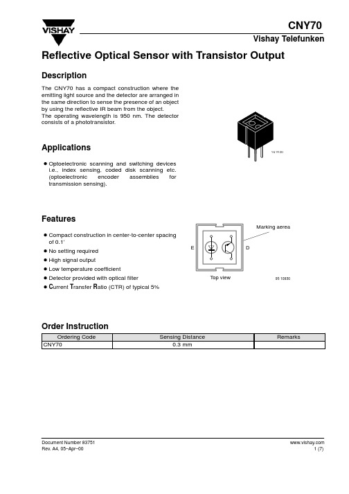
Dimensions of CNY70 in mm95 11345www.vishay.Document Number 83751Ozone Depleting Substances Policy StatementIt is the policy of Vishay Semiconductor GmbH to1.Meet all present and future national and international statutory requirements.2.Regularly and continuously improve the performance of our products, processes, distribution and operatingsystems with respect to their impact on the health and safety of our employees and the public, as well as their impact on the environment.It is particular concern to control or eliminate releases of those substances into the atmosphere which are known as ozone depleting substances (ODSs).The Montreal Protocol (1987) and its London Amendments (1990) intend to severely restrict the use of ODSs and forbid their use within the next ten years. Various national and international initiatives are pressing for an earlier ban on these substances.Vishay Semiconductor GmbH has been able to use its policy of continuous improvements to eliminate the use of ODSs listed in the following documents.1.Annex A, B and list of transitional substances of the Montreal Protocol and the London Amendments respectively2.Class I and II ozone depleting substances in the Clean Air Act Amendments of 1990 by the EnvironmentalProtection Agency (EPA) in the USA3.Council Decision 88/540/EEC and 91/690/EEC Annex A, B and C (transitional substances) respectively. Vishay Semiconductor GmbH can certify that our semiconductors are not manufactured with ozone depleting substances and do not contain such substances.We reserve the right to make changes to improve technical design and may do so without further notice. Parameters can vary in different applications. All operating parameters must be validated for each customer application by the customer. Should the buyer use Vishay Telefunken products for any unintended or unauthorized application, the buyer shall indemnify Vishay Telefunken against all claims, costs, damages, and expenses, arising out of, directly or indirectly, any claim of personal damage, injury or death associated with such unintended or unauthorized use.Vishay Semiconductor GmbH, P.O.B. 3535, D-74025 Heilbronn, GermanyTelephone: 49 (0)7131 67 2831, Fax number: 49 (0)7131 67 2423Document Number 83751。
乐泰SF 7070 known as Loctite 7070 安全技术说明书

安全技术说明书根据GB/T 16483-2008第 1 页 共 7 页LOCTITE SF 7070 known as Loctite 7070安全技术说明书编号 : 153660V 001.14修订: 07.05.2013 发布日期: 11.09.2018化学品中文名称: LOCTITE SF 7070 known as Loctite 7070 推荐用途: 溶剂基清洁剂企业信息:汉高(中国)投资有限公司 张衡路928号 201203 中国上海市浦东新区中国电话: +86-21-2891 8000 传真:+86-21-2891 5137生效日期: 07.05.2013应急信息: 应急电话:+86 532 8388 9090 (24小时)。
物质或混合物的分类根据GB 13690-2009 (化学品分类和危险性公示通则):危险分类 危险类别 接触途径 靶器官 易燃液体 第3类皮肤敏化作用 第1A 类 皮肤接触 皮肤刺激 第2类 皮肤接触 吸入危害第1类 对水生环境有慢性危害第2类标签要素根据GB 15258-2009 (化学品安全标签编写规定):象形图:信号词:危险危险性说明:H226 易燃液体和蒸气。
H304 吞咽并进入呼吸道可能致命。
H315 造成皮肤刺激。
H317 可能导致皮肤过敏反应H411 对水生生物有毒并具有长期持续影响。
防范说明(预防):P210远离热源/火花/明火。
-禁止吸烟。
P233保持容器密闭。
P240容器和接收设备接地/等势联接。
P241P241:使用防爆的电气设备。
P243采取防止静电放电的措施。
P261避免吸入喷雾。
P264处理后要彻底洗手P271只能在室外或通风良好之处使用。
P273避免释放到环境中。
P280戴防护手套/穿防护服/戴防护眼罩/戴防护面具。
防范说明(响应):P301+P310如误吞咽:立即呼叫解毒中心或医生。
P302+P352如皮肤沾染:用大量肥皂和水清洗。
产品7070
中国上海市延安东路 618 号东海商业中心二期 3F
邮编 :200001
.
电话 :86.21.53534595
传真 :86.21.53854259
Loctite® 乐泰® 是美国乐泰公司注册商标
使用指南 1. 在处理表面大量喷涂。 2. 趁湿用净布除去表面污染物。如有必要,再次
S
氯丁橡胶 +2.3
S +14.7
S
PU 硅胶
+0.07
SS +3.30
S
+13.8
S +17.7
S
Viton®
0
SS +3.10
S
干燥速度 25°C 下干燥时间
材料 不擦 后擦(干布)
分钟 5-20 1-2
环境信息 7070 不含臭氧破坏成分,不同于 1.1.1-三氯乙烷。 本产品不在 1990 干净空气行动法案或蒙特利尔条约 之列,不会收到控制而取缔。本产品不含 SARAIII,313 章中成分。TSCA 用于美国,DSL 用 于加拿大。
NC
并非产品规格 以下所含技术资料仅供参考 请与 LOCTITE 公司技术部门联系, 以便获得该产品规格方面的支持与建议。
塑料
ABS 丙烯酸 Delrin® 环氧树脂 G10 尼龙 101 尼龙 66 PC 酚醛 聚乙烯(高密) 聚乙烯(低密) 聚丙烯 聚苯乙烯 (高冲击) 聚苯乙烯 聚砜 PVC 特氟龙® Ultem® Valox®420
SS +1.72
S
S +11.3
S
SS +1.73
S
7070
1,1,1-三氯乙烷
38°C 下 30 分钟 38°C 下 30 分钟
HT7050a规格书
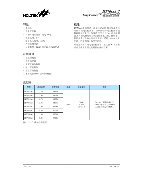
Rev. 1.4012014-03-19• 低功耗• 低温度系数• 高输入电压范围 (高达 30V)• 静态电流:3µA • 输出电压精度:±1%• 内建迟滞电路• 封装类型:TO92, SOT89 和 SOT23-5应用领域• 电池检测器• 电平选择器• 电源故障检测器• 微计算机复位• 电池存储备份• 非易失性RAM 信号存储保护HT70xxA-2系列是一组采用CMOS 技术实现的三端低功耗电压检测器。
该系列中的电压检测器能检测固定的电压,范围从 2.2V 到 8.2V 。
电压检测器系列由高精度低功耗的标准电压源、比较器、迟滞电路以及输出驱动器组成。
采用 CMOS 技术制造,因而确保了低功率消耗。
尽管主要用作固定电压检测器,但这些 IC 可搭配外部元件用于指定的阈值电压的检测。
选型表注:“xx ” 代表检测电压。
Rev. 1.4022014-03-19deN 沟道开漏输出(常开,低有效)输出表格和曲线图...d...引脚图电源供应电压 .............................................................................................................................V SS-0.3V ~ V SS+33V 输出电压 ...................................................................................................................................V SS-0.3V ~ V DD+0.3V 输出电流 .............................................................................................................................................................50mA功耗 ..................................................................................................................................................................200mW 储存温度范围 ............................................................................................................................................................−50°C ~ 125°C 工作环境温度 ........................................................................................................................................−40°C ~ 85°C 注:这里只强调额定功率,超过极限参数所规定的范围将对芯片造成损害,无法预期芯片在上述标示范围外的工作状态,而且若长期在标示范围外的条件下工作,可能影响芯片的可靠性。
2A07-T中文资料

e 32A01 - 2A072.0A RECTIFIERFeaturesMaximum Ratings and Electrical Characteristics@ T A = 25°C unless otherwise specified·Diffused Junction·High Current Capability and Low Forward Voltage Drop ·Surge Overload Rating to 70A Peak·Lead Free Finish, RoHS Compliant (Note 3)Mechanical Data·Case: DO-15·Case Material: Molded Plastic. UL Flammability Classification Rating 94V-0·Moisture Sensitivity: Level 1 per J-STD-020C·Terminals: Finish – Bright Tin. Solderable per MIL-STD-202,Method 208·Polarity: Cathode Band ·Marking: Type Number·Weight: 0.4 grams (approximate)Single phase, half wave, 60Hz, resistive or inductive load.For capacitive load, derate current by 20%.Notes: 1. Leads maintained at ambient temperature at a distance of 9.5mm from the case.2. Measured at 1.0 MHz and Applied Reverse Voltage of 4.0V DC.3. RoHS revision 13.2.2003. Glass and High Temperature Solder Exemptions Applied, see EU Directive Annex Notes 5 and 7.0.010.11.0100.40.8 1.21.6I ,I N S T A N T A N E O U S F O R W A R D C U R R E N T (A )F VF,INSTANTANEOUS FORWARD VOLTAGE (V)Fig.2Typical Forward Characteristics1.0101001.010100C ,T O T A L C A P A C I T A N C E (p F )T V ,REVERSE VOLTAGE (V)Fig.4Typical Total CapacitanceR 02.5I ,A V E R A G E F O R W A R D R E C T I F I E D C U R R E N T (A )O T ,AMBIENT TEMPERATURE (ºC)Fig.1Forward Current Derating CurveA 2550751001251501752000.51.01.52.0110100I ,P E A K F O R W A R D S U R G E C U R R E N T (A )F S M NUMBER OF CYCLES AT 60HzFig.3Max Non-Repetitive Peak Fwd SurgeCurrent03060754515Ordering InformationNotes:4.For packaging details, visit our website at /datasheets/ap02008.pdf.(Note 4)IMPORTANT NOTICEDiodes Incorporated and its subsidiaries reserve the right to make modifications,enhancements,improvements,corrections or other changes without further notice to any product herein.Diodes Incorporated does not assume any liability arising out of the application or use of any product described herein;neither does it convey any license under its patent rights,nor the rights of others.The user of products in such applications shall assume all risks of such use and will agree to hold Diodes Incorporated and all the companies whose products are represented on our website,harmless against all damages.LIFE SUPPORTDiodes Incorporated products are not authorized for use as critical components in life support devices or systems without the expressed written approval of the President of Diodes Incorporated.。
- 1、下载文档前请自行甄别文档内容的完整性,平台不提供额外的编辑、内容补充、找答案等附加服务。
- 2、"仅部分预览"的文档,不可在线预览部分如存在完整性等问题,可反馈申请退款(可完整预览的文档不适用该条件!)。
- 3、如文档侵犯您的权益,请联系客服反馈,我们会尽快为您处理(人工客服工作时间:9:00-18:30)。
7000M Chassis/ Power Supply 7000S Standby Power Supply
7000M Chassis/ Power Supply 7000S Standby Power Supply 7070T Satellite Modem Video Modulator Exciter
E-mail: sales@ Website:
Ordering Information
Description 7070 Fiberoptic Transmitter 7070 Fiberoptic Receiver Option - Standalone Option - 50Ω Order Code 7070T 7070R add - STD add - 50
HPA
C or Ku Up Converter
7070R
Fiber
System 7070 IFL- IF Fiberoptic Interfacility Link
Sadna/graphic design 3/2000 LNB C or Ku Down Converter 7070T Fiber Antenna Site Control Room 7070R
Order Code 7000M 7000s APC-J-5 2000 7050-4 2100
All specs are subject to change wihout prior notபைடு நூலகம்ce.
© Foxcom 2000. Doc. No. 13-002-04D
For longer distances contact Foxcom
10 - 200 MHz ±0.2 dB @ 36 MHz/ ±1.5dB @ full band 75 Ohm (50 optional) 16 dB 50 dB @ 1 MHz BW / 5 Km -40 dBc -40 to -20 dBm -45 to -15 dBm 0±10 dB BNC
Physical Chassis Capacity Chassis Size Unit Size Power for Rackmount Chassis Transmitter Receiver Operating Temp. Range Storage Temp. Range 6 plug-ins 19" x 5.25" x 7" 5" x 4.8" x 1.6" 110 or 220 VAC. 50/ 60Hz, 60 Watts (max.) 15 VDC @ 400 mA (max.) 15 VDC @ 300 mA (max.) -10˚C to 60˚C -40˚C to 85˚C
Optical Characteristics Optical Wavelength Optical Power Output Optical Connector Optical Budget Optical Return Loss Single Mode Fiber Loss 1310 ±10nm -3 dBm (min.) FC/APC 6 dB 60 dBc (min.) 0.4 dB/km
Specs apply for fusion spliced singlemode fiber (9/125 micron) with low reflection FC/APC connectors.
SAT-LIGHT™ - High Performance, Cost Effective Interfacility Links
70/140 MHz IF transmission Flat frequency response from 10 - 200 MHz Protocol transparent - transmits all video, audio and digital formats Signal transmission ranging from 100 meters to 10 kilometers Test ports, indicators, alarms and monitors Selectable Manual or Automatic Gain Control
Available Accessories Chassis and Power Supply Redundant Power Supply 110 VAC FC/APC 5m Jumper Cable 1:1 Redundant Switch Asynchronous Data Link 32 dB Broadband
Satellite Modem VSAT Terminal Tracking Receiver
7070 - System Specifications
RF Characteristics Frequency Range Flatness Input/Output Impedance Input/Output Return Loss Carrier to Noise IMD Input Signal Range (Total Power) Output Signal Range (Total Power) Link Gain RF connector
The 7070 IFL is a 10 - 200 MHz interfacility fiberoptic link used primarily in single channel IF signal uplinking applications with medium dynamic range requirements. The 7070 IFL consists of an optical transmitter (7070T) that receives signals from satellite modems, video modulators, or exicters and transmits them to an optical receiver (7070R) via singlemode fiber. The 7070T and 7070R modules plug into a 7000M 3U chassis/power supply that enables expansion of the system to accommodate any 6 SAT-LIGHT® modules. A wide variety of options are available. The 7070 IFL transmits all satellite modulation schemes - digital or analog. The RF signal is directly modulated and adds virtually no phase noise to the original IF signal. The direct modulation, along with extremely flat amplitude and group delay guarantees low BER and high signal quality, independent of distance. 7070 IFL offers a choice of gain control. Applications requiring unity gain use Manual Gain Control (MGC), while downlink applications use Automatic Gain Control for constant output over a wide range of signal levels. Front panel test ports, LEDs and back panel monitors and alarms allow for complete system status monitoring and for interfacing with M&C systems.