BD5413EFV中文资料
IDT54FCT138CTD中文资料

The IDT54/74FCT138T/AT/CT are 1-of-8 decoders built using an advanced dual metal CMOS technology. The IDT54/74FCT138T/AT/CT accepts three binary weighted inputs (A 0,A 1, A 2) and, when enabled, provides eight mutually exclusive active LOW outputs (O 0-O 7). The IDT54/74FCT138T/AT/CT features three enable inputs, two active LOW (E 1, E 2) and one active HIGH (E 3). All outputs will be HIGH unless E 1 and E 2 are LOW and E 3 is HIGH. This multiple enable function allows easy parallel expansion of the device to a 1-of-32 (5 lines to 32 lines) decoder with just four IDT54/74FCT138T/AT/CT devices and one inverter.FUNCTIONAL BLOCK DIAGRAM2570 drw 012570 drw 022570 drw 03PIN CONFIGURATIONSO 6O 2LCC TOP VIEWO 1NC O 3O 4O 7O 5G N D N CMILITARY AND COMMERCIAL TEMPERATURE RANGESAPRIL 1995O 7O 6O 5O 4O 3O 2O 1O 0A 2A 1A 0E 1E 2E 3GNDA 0O 0O 6V CC DIP/SOIC/QSOP/CERPACKTOP VIEWA 1A 2E 1E 2E 37O 1O 2O 3O 4O 5•Std., A and C speed grades•Low input and output leakage ≤1µA (max.)•CMOS power levels•True TTL input and output compatibility – V OH = 3.3V (typ.)– V OL = 0.3V (typ.)•High drive outputs (-15mA I OH , 48mA I OL )•Meets or exceeds JEDEC standard 18 specifications •Product available in Radiation Tolerant and Radiation Enhanced versions•Military product compliant to MIL-STD-883, Class B and DESC listed (dual marked)•Available in DIP, SOIC, QSOP, CERPACK and LCC packagesThe IDT logo is a registered trademark of Integrated Device Technology, Inc.FUNCTION TABLE2570 tbl 02(1)2570 tbl 011.Stresses greater than those listed under ABSOLUTE MAXIMUM RAT-INGS may cause permanent damage to the device. This is a stress rating only and functional operation of the device at these or any other conditions above those indicated in the operational sections of this specification is not implied. Exposure to absolute maximum rating conditions for extended periods may affect reliability. No terminal voltage may exceed V CC by +0.5V unless otherwise noted.2.Input and V CC terminals only.3.Outputs and I/O terminals only.1. This parameter is measured at characterization but not tested.DC ELECTRICAL CHARACTERISTICS OVER OPERATING RANGEFollowing Conditions Apply Unless Otherwise Specified:1.For conditions shown as Max. or Min., use appropriate value specified under Electrical Characteristics for the applicable device type.2.Typical values are at V CC = 5.0V, +25°C ambient.3.Not more than one output should be shorted at one time. Duration of the short circuit test should not exceed one second.4.The test limit for this parameter is ±5µA at T A = –55°C.1.For conditions shown as Max. or Min., use appropriate value specified under Electrical Characteristics for the applicable device type.2.Typical values are at V CC = 5.0V, +25°C ambient.3.Per TTL driven input (V IN = 3.4V). All other inputs at V CC or GND.4.This parameter is not directly testable, but is derived for use in Total Power Supply Calculations.5.Values for these conditions are examples of the I CC formula. These limits are guaranteed but not tested.6.I C = I QUIESCENT + I INPUTS + I DYNAMICI C = I CC + ∆I CC D H N T + I CCD (f o N o)I CC = Quiescent Current∆I CC = Power Supply Current for a TTL High Input (V IN = 3.4V)D H = Duty Cycle for TTL Inputs HighN T = Number of TTL Inputs at D HI CCD = Dynamic Current Caused by an Input Transition Pair (HLH or LHL)f o = Output FrequencyN o = Number of Outputs at f oAll currents are in milliamps and all frequencies are in megahertz.2570 tbl 071.See test circuit and waveforms.2.Minimum limits are guaranteed but not tested on Propagation Delays.TEST CIRCUITS AND WAVEFORMS TEST CIRCUITS FOR ALL OUTPUTSENABLE AND DISABLE TIMESPROPAGATION DELAY7.0V3V 1.5V 0V3V 1.5V 0V 3V 1.5V 0V 3V 1.5V 0V DATA INPUTPRESET CLEAR ETC.1.5V1.5VSAME PHASE INPUT TRANSITION3V 1.5V 0V 1.5V V OH OUTPUTOPPOSITE PHASE INPUT TRANSITION3V 1.5V 0VV OL 3V1.5V 0V 3.5V 0VV OLENABLEDISABLEV OH PRESET CLEARCLOCK ENABLEETC.SET-UP, HOLD AND RELEASE TIMES PULSE WIDTHC L =Load capacitance: includes jig and probe capacitance.R T =Termination resistance: should be equal to Z OUT of the PulseGenerator.2570 drw 042570 drw 062570 drw 052570 drw 08NOTES:1.Diagram shown for input Control Enable-LOW and input Control Disable-HIGH2.Pulse Generator for All Pulses: Rate ≤ 1.0MHz; t F ≤ 2.5ns; t R ≤ 2.5ns2570 drw 07ORDERING INFORMATIONIDT XX FCT138T138AT138CT1-of-8 Decoder54 74–55°C to +125°C 0°C to +70°CTemp. RangeXXXXDevice TypeXPackageXProcessBlankBPDSOELQCommercialMIL-STD-883, Class BPlastic DIPCERDIPSmall Outline ICCERPACKLeadless Chip CarrierQuarter-size Small Outline Package XFamilyBlankHigh Drive2570 drw 09。
7413中文资料

100
VDS VGS RG
RD D.U.T.
10V
Pulse Width ≤ 1 µs Duty Factor ≤ 0.1 %
+-VDD
Fig 10a. Switching Time Test Circuit
VDS 90%
10% VGS
td(on) tr
td(off) tf
Fig 10b. Switching Time Waveforms
tr td(off) tf Ciss
Rise Time Turn-Off Delay Time Fall Time Input Capacitance
––– 8.0 ––– ns ID = 7.2A
––– 35 –––
RG = 6.2Ω
––– 14 –––
VGS = 10V
––– 1670 –––
Benefits
l Low Gate to Drain Charge to Reduce
S
1
Switching Losses
l Fully Characterized Capacitance Including S 2
AA
8
D
7
D
Effective COSS to Simplify Design, (See
Max. 12 9.6 96 2.5 0.02 ± 20 1.0
-55 to + 150
300 (1.6mm from case )
Units
A
W W/°C
V V/ns
°C
Thermal Resistance
Symbol RθJL RθJA
Parameter Junction-to-Drain Lead Junction-to-Ambient
CD4013中文资料
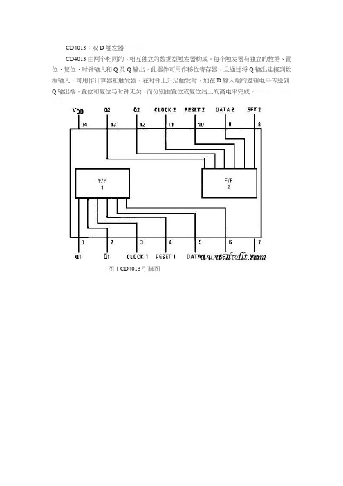
CD4013:双D触发器CD4013由两个相同的、相互独立的数据型触发器构成。
每个触发器有独立的数据、置位、复位、时钟输入和Q及Q输出,此器件可用作移位寄存器,且通过将Q输出连接到数据输入,可用作计算器和触发器。
在时钟上升沿触发时,加在D输入端的逻辑电平传送到Q输出端。
置位和复位与时钟无关,而分别由置位或复位线上的高电平完成。
图1CD4013引脚图图2CD4013内部电路图图3 CD4013逻辑图Truth Table 真值表功能:Absolute Maximum Ratings 绝对最大额定值:Recommended Operating Conditions 建议操作条件:DC Electrical Characteristics 直流电气特性:AC Electrical Characteristics 交流电气特性:65120tTHL, tTLHTransition Time过渡时间VDD = 5V100200nsVDD = 10V50100VDD = 15V4080tWL, tWHMinimum Clock Pulse Width最小时钟脉冲宽度VDD = 5V100200nsVDD = 10V4080VDD = 15V3265tRCL, tFCLMaximum Clock Rise and Fall Time最大时钟上升和下降时间VDD = 5V15 msVDD = 10V10VDD = 15V5tSUMinimum Set-Up Time 最低设置时间VDD = 5V2040nsVDD = 10V1530VDD = 15V1225fCLMaximum Clock Frequency 最大时钟频率VDD = 5V2.55MHzVDD = 10V6.212.5VDD = 15V7.615.5SET AND RESET OPERATION SET和复位操作tPHL(R),tPLH(S)Propagation Delay Time传递延迟时间VDD = 5V150 300ns VDD = 10V45130 VDD = 15V6590tWH(R), tWH(S)Minimum Set and Reset Pulse Width最低限度和复位脉冲宽度VDD = 5V90180 nsVDD = 10V 40 80VDD = 15V2550CINAverage Input Capacitance 平均输入电容Any Input57.5pF图4 切换时间波形应用电路:置位和复位电路图5(左)和图(右)中的CD4013是CMOS双D触发器,这类电路置位和复位信号是高电平有效,由于开关闭合时电容可视为短路而产生高电平,使RD=1,Q=0;若将此信号加到SD,则SD=1,Q=1;置位、复位过后,电容充电而使RD(SD)变为0,电路可进入计数状态。
SN54AHCT541中文资料

PACKAGING INFORMATIONOrderable Device Status(1)PackageType PackageDrawingPins PackageQtyEco Plan(2)Lead/Ball Finish MSL Peak Temp(3)5962-9685801Q2A ACTIVE LCCC FK201TBD Call TI Level-NC-NC-NC 5962-9685801QRA ACTIVE CDIP J201TBD Call TI Level-NC-NC-NC 5962-9685801QSA ACTIVE CFP W201TBD Call TI Level-NC-NC-NC SN74AHCT541DBLE OBSOLETE SSOP DB20TBD Call TI Call TISN74AHCT541DBR ACTIVE SSOP DB202000Green(RoHS&no Sb/Br)CU NIPDAU Level-1-260C-UNLIMSN74AHCT541DBRE4ACTIVE SSOP DB202000Green(RoHS&no Sb/Br)CU NIPDAU Level-1-260C-UNLIMSN74AHCT541DW ACTIVE SOIC DW2025Green(RoHS&no Sb/Br)CU NIPDAU Level-1-260C-UNLIMSN74AHCT541DWE4ACTIVE SOIC DW2025Green(RoHS&no Sb/Br)CU NIPDAU Level-1-260C-UNLIMSN74AHCT541DWR ACTIVE SOIC DW202000Green(RoHS&no Sb/Br)CU NIPDAU Level-1-260C-UNLIMSN74AHCT541DWRE4ACTIVE SOIC DW202000Green(RoHS&no Sb/Br)CU NIPDAU Level-1-260C-UNLIMSN74AHCT541N ACTIVE PDIP N2020Pb-Free(RoHS)CU NIPDAU Level-NC-NC-NCSN74AHCT541NE4ACTIVE PDIP N2020Pb-Free(RoHS)CU NIPDAU Level-NC-NC-NCSN74AHCT541NSR ACTIVE SO NS202000Green(RoHS&no Sb/Br)CU NIPDAU Level-1-260C-UNLIMSN74AHCT541NSRE4ACTIVE SO NS202000Green(RoHS&no Sb/Br)CU NIPDAU Level-1-260C-UNLIMSN74AHCT541PW ACTIVE TSSOP PW2070Green(RoHS&no Sb/Br)CU NIPDAU Level-1-260C-UNLIMSN74AHCT541PWE4ACTIVE TSSOP PW2070Green(RoHS&no Sb/Br)CU NIPDAU Level-1-260C-UNLIM SN74AHCT541PWLE OBSOLETE TSSOP PW20TBD Call TI Call TISN74AHCT541PWR ACTIVE TSSOP PW202000Green(RoHS&no Sb/Br)CU NIPDAU Level-1-260C-UNLIMSN74AHCT541PWRE4ACTIVE TSSOP PW202000Green(RoHS&no Sb/Br)CU NIPDAU Level-1-260C-UNLIMSN74AHCT541PWRG4ACTIVE TSSOP PW202000Green(RoHS&no Sb/Br)CU NIPDAU Level-1-260C-UNLIM SNJ54AHCT541FK ACTIVE LCCC FK201TBD Call TI Level-NC-NC-NC SNJ54AHCT541J ACTIVE CDIP J201TBD Call TI Level-NC-NC-NC SNJ54AHCT541W ACTIVE CFP W201TBD Call TI Level-NC-NC-NC (1)The marketing status values are defined as follows:ACTIVE:Product device recommended for new designs.LIFEBUY:TI has announced that the device will be discontinued,and a lifetime-buy period is in effect.NRND:Not recommended for new designs.Device is in production to support existing customers,but TI does not recommend using this part in a new design.PREVIEW:Device has been announced but is not in production.Samples may or may not be available.OBSOLETE:TI has discontinued the production of the device.(2)Eco Plan-The planned eco-friendly classification:Pb-Free(RoHS)or Green(RoHS&no Sb/Br)-please check /productcontent for the latest availability information and additional product content details.TBD:The Pb-Free/Green conversion plan has not been defined.Pb-Free(RoHS):TI's terms"Lead-Free"or"Pb-Free"mean semiconductor products that are compatible with the current RoHS requirements for all6substances,including the requirement that lead not exceed0.1%by weight in homogeneous materials.Where designed to be soldered at high temperatures,TI Pb-Free products are suitable for use in specified lead-free processes.Green(RoHS&no Sb/Br):TI defines"Green"to mean Pb-Free(RoHS compatible),and free of Bromine(Br)and Antimony(Sb)based flame retardants(Br or Sb do not exceed0.1%by weight in homogeneous material)(3)MSL,Peak Temp.--The Moisture Sensitivity Level rating according to the JEDEC industry standard classifications,and peak solder temperature.Important Information and Disclaimer:The information provided on this page represents TI's knowledge and belief as of the date that it is provided.TI bases its knowledge and belief on information provided by third parties,and makes no representation or warranty as to the accuracy of such information.Efforts are underway to better integrate information from third parties.TI has taken and continues to take reasonable steps to provide representative and accurate information but may not have conducted destructive testing or chemical analysis on incoming materials and chemicals.TI and TI suppliers consider certain information to be proprietary,and thus CAS numbers and other limited information may not be available for release.In no event shall TI's liability arising out of such information exceed the total purchase price of the TI part(s)at issue in this document sold by TI to Customer on an annual basis.元器件交易网IMPORTANT NOTICETexas Instruments Incorporated and its subsidiaries (TI) reserve the right to make corrections, modifications,enhancements, improvements, and other changes to its products and services at any time and to discontinueany product or service without notice. Customers should obtain the latest relevant information before placingorders and should verify that such information is current and complete. All products are sold subject to TI’s termsand conditions of sale supplied at the time of order acknowledgment.TI warrants performance of its hardware products to the specifications applicable at the time of sale inaccordance with TI’s standard warranty. T esting and other quality control techniques are used to the extent TIdeems necessary to support this warranty. Except where mandated by government requirements, testing of allparameters of each product is not necessarily performed.TI assumes no liability for applications assistance or customer product design. Customers are responsible fortheir products and applications using TI components. T o minimize the risks associated with customer productsand applications, customers should provide adequate design and operating safeguards.TI does not warrant or represent that any license, either express or implied, is granted under any TI patent right,copyright, mask work right, or other TI intellectual property right relating to any combination, machine, or processin which TI products or services are used. Information published by TI regarding third-party products or servicesdoes not constitute a license from TI to use such products or services or a warranty or endorsement thereof.Use of such information may require a license from a third party under the patents or other intellectual propertyof the third party, or a license from TI under the patents or other intellectual property of TI.Reproduction of information in TI data books or data sheets is permissible only if reproduction is withoutalteration and is accompanied by all associated warranties, conditions, limitations, and notices. Reproductionof this information with alteration is an unfair and deceptive business practice. TI is not responsible or liable forsuch altered documentation.Resale of TI products or services with statements different from or beyond the parameters stated by TI for thatproduct or service voids all express and any implied warranties for the associated TI product or service andis an unfair and deceptive business practice. TI is not responsible or liable for any such statements.Following are URLs where you can obtain information on other Texas Instruments products and applicationsolutions:Products ApplicationsAmplifiers Audio /audioData Converters Automotive /automotiveDSP Broadband /broadbandInterface Digital Control /digitalcontrolLogic Military /militaryPower Mgmt Optical Networking /opticalnetworkMicrocontrollers Security /securityTelephony /telephonyVideo & Imaging /videoWireless /wirelessMailing Address:Texas InstrumentsPost Office Box 655303 Dallas, Texas 75265Copyright 2005, Texas Instruments Incorporated。
hef4013bp中文资料

hef4013bp中文资料篇一:hef4013中文手册它是由具有Set和复位的2个D型触发器构成的。
对D输入施加的信息以时钟脉冲的低电平读入以高电平传输到输出Q。
引脚主要功能引脚主要功能1数据出182数据出193时钟入1104清除入115数据入1126置位入1137电源地14置位入2数据入2清除入时钟入2数据出2数据出2电源篇二:TC4013双D触发器TC4013与CD4013广东湛江莱德电器维修中心编辑整理2022-12-5TC4013双D触发电路【性能参数】双列14脚封装,金属-氧化物-半导体型互补MOS,电源电压Vdd=-0.5~18V;输入电压Vi=-0.5~Vdd+0.5V;输出引脚电压Vo=-0.5~Vdd+0.5V;峰值输入,输出端电流±Ii=10mA;允许功耗Pd=100mW。
【互换兼容】CD4013C4013HD14013MSM4013MC14013HEF4013CC4013CH4013CM4013HCC401 3HCF4013C043BF4013CH4013ACH4013BCH4013CLC4013ZC4013AZC4013BZC40 13CSCL4013DG4013TC4013BP是一个双D触发器,功能和CMOS的CD4013和TTL的74LS74是一样的附图是功能引脚图篇三:四路红外控制器电路四路红外控制器电路一、功能说明四路红外控制电路主要由红外编码发射部分和红外解码接收、控制部分组成,编码和解码芯片分别采用PT2262-IR和PT2272-M4,发射和接收地址编码设置必须完全一致才能配对使用。
发射电路用来发射38KHz的红外载波,将编码后的地址码、数据码、同步码随同载波一起发射出去;接收电路接收到有效信号,经过处理、解码后变成所需的电信号(当解码芯片PT2272接收发送过来的信号时,VT 脚输出一个正脉冲,与此同时,相应的数据脚也输出高电平),通过HEF4013BP控制继电器的吸合和断开。
MUN5313DW1T1G中文资料

Characteristic
Symbol
Min
Typ
ON CHARACTERISTICS (Note 4) DC Current Gain
(VCE = 10 V, IC = 5.0 mA)
Collector-Emitter Saturation Voltage (IC = 10 mA, IB = 0.3 mA)
hFE
35
60
60
100
80
140
80
140
160
350
160
350
3.0
5.0
8.0
15
15
30
80
200
80
150
80
140
VCE(sat)
MUN5311DW1T1
−
−
MUN5312DW1T1
−
−
MUN5313DW1T1
−
−
MUN5314DW1T1
−
−
MUN5335DW1T1
−
−
MUN5330DW1T1
MUN5315DW1T1
SOT−363
MUN5315DW1T1G
SOT−363
15
10
∞
(Pb−Free)
MUN5316DW1T1
SOT−363
MUN5316DW1T1G
SOT−363
16
4.7
∞
MUN5330DW1T1
(Pb−Free) SOT−363
3000/Tape & Reel
MUN5330DW1T1G
MAXIMUM RATINGS (TA = 25°C unless otherwise noted, common for Q1 and Q2, − minus sign for Q1 (PNP) omitted)
PI3HDMI341ARTFFE中文资料

Pin Description
Pin # 6,9,12,15 68, 71, 74, 77 49, 52, 55, 58 5, 8, 11, 14 67, 70, 73, 76 48, 51, 54, 57 4, 10, 16 24, 30, 36, 37, 47, 53, 59, 65, 66, 72, 78 80 62 44 40 Pin Name A11, A12, A13, A14 A21, A22, A23, A24 A31, A32, A33, A34 B11, B12, B13, B14 B21, B22, B23, B24 B31, B32, B33, B34 GND HPD1 HPD2 HPD3 HPD_Sink O O O I I/O I I I I I I Description Port 1 TMDS Positive inputs Port 2 TMDS Positive inputs Port 3 TMDS Positive inputs Port 1 TMDS Negative inputs Port 2 TMDS Negative inputs Port 3 TMDS Negative inputs Ground Port 1 HPD output Port 2 HPD output Port 3 HPD output Sink side hot plug detector input. High: 5-V power signal asserted from source to sink and EDID is ready. Low: No 5-V power signal asserted from source to sink, or EDID is not ready. Output Enable, Active LOW Port 1 DDC Clock Port 2 DDC Clock Port 3 DDC Clock Sink Side DDC Data Port 1 DDC Data Port 2 DDC Data Port 3 DDC Data Sink Side DDC Data Source Input Selector 3.3V Power Supply O O I I TMDS positive outputs TMDS negative outputs Equalizer controls(1) Output buffer controls Note: OC_S3 has an internal pull-up resistor. OC_S2 has an internal pull-down resistor.
CC2541中文资料_数据手册_参数

ZHCS708D – JANUARY 2012 – REVISED JUNE 2013
2.4-GHz Bluetooth™ 低能耗和私有片载系统
查询样品: CC2541
特性
1
• 射频 23 – 2.4-GHz Bluetooth 符合低能耗规范和私有的 RF 片载系统 – 支持 250-kbps,500-kbps,1-Mbps,2-Mbps 的数据速率
版权 © 2012–2013, Texas Instruments Incorporated English Data Sheet: SWRS110
CC2541
ZHCS708D – JANUARY 2012 – REVISED JUNE 2013
软件特性
• 符合针对单模式蓝牙低能耗 (BLE) 解决方案的符 合Bluetooth v4.0 协议的堆栈 – 完全功率优化堆栈,包括控制器和主机 – GAP - 中心设备,外设,或者广播器(包括 组合角色) – 属性协议 (ATT) / 通用属性配置文件 (GATT) – 客户端和服务器 – 对称式对多重处理 (SMP) - AES-128 加密和 解密 – L2CAP – 示例应用和配置文件 – 针对 GAP 中心和外围作用的一般应用 – 距离临近,加速计,简单关键字,和电池 GATT 服务 – BLE 软件栈 内支持更多应用 – 多重配置选项 – 单芯片配置,允许应用运行在 CC2541 上 – 用于运行在一个外部微处理器上的网络处理 器接口 – BTool - 用于评估、开发和测试的视窗 (Windows) PC 应用
• 低功率 – 工作模式 RX 低至: 17.9 mA – 工作模式 TX (0 dBm): 18.2 mA – 功率模式 1 (4-µs 唤醒): 270 µA – 功率模式 2 (睡眠定时器打开): 1 µA – 功率模式 3 (外部中断): 0.5 µA – 宽泛的电源电压范围 (2 V–3.6 V)
- 1、下载文档前请自行甄别文档内容的完整性,平台不提供额外的编辑、内容补充、找答案等附加服务。
- 2、"仅部分预览"的文档,不可在线预览部分如存在完整性等问题,可反馈申请退款(可完整预览的文档不适用该条件!)。
- 3、如文档侵犯您的权益,请联系客服反馈,我们会尽快为您处理(人工客服工作时间:9:00-18:30)。
Notes
No technical content pages of this document may be reproduced in any form or transmitted by any means without prior permission of ROHM CO.,LTD. The contents described herein are subject to change without notice. The specifications for the product described in this document are for reference only. Upon actual use, therefore, please request that specifications to be separately delivered. Application circuit diagrams and circuit constants contained herein are shown as examples of standard use and operation. Please pay careful attention to the peripheral conditions when designing circuits and deciding upon circuit constants in the set. Any data, including, but not limited to application circuit diagrams information, described herein are intended only as illustrations of such devices and not as the specifications for such devices. ROHM CO.,LTD. disclaims any warranty that any use of such devices shall be free from infringement of any third party's intellectual property rights or other proprietary rights, and further, assumes no liability of whatsoever nature in the event of any such infringement, or arising from or connected with or related to the use of such devices. Upon the sale of any such devices, other than for buyer's right to use such devices itself, resell or otherwise dispose of the same, no express or implied right or license to practice or commercially exploit any intellectual property rights or other proprietary rights owned or controlled by ROHM CO., LTD. is granted to any such buyer. Products listed in this document are no antiradiation design.
ROHM Customer Support System
Copyright © 2007 ROHM CO.,LTD.
THE AMERICAS / EUPOPE / ASIA / master@ rohm.co. jp
21, Saiin Mizosaki-cho, Ukyo-ku, Kyoto 615-8585, Japan
TEL : +81-75-311-2121 FAX : +81-75-315-0172
Appendix1-Rev2.0
Thank you for your accessing to ROHM product informations. More detail product informations and catalogs are available, please contact your nearest sales office.
The products listed in this document are designed to be used with ordinary electronic equipment or devices (such as audio visual equipment, office-automation equipment, communications devices, electrical appliances and electronic toys). Should you intend to use these products with equipment or devices which require an extremely high level of reliability and the malfunction of which would directly endanger human life (such as medical instruments, transportation equipment, aerospace machinery, nuclear-reactor controllers, fuel controllers and other safety devices), please be sure to consult with our sales representative in advance. It is our top priority to supply products with the utmost quality and reliability. However, there is always a chance of failure due to unexpected factors. Therefore, please take into account the derating characteristics and allow for sufficient safety features, such as extra margin, anti-flammability, and fail-safe measures when designing in order to prevent possible accidents that may result in bodily harm or fire caused by component failure. ROHM cannot be held responsible for any damages arising from the use of the products under conditions out of the range of the specifications or due to non-compliance with the NOTES specified in this catalog.