2SC4300中文资料
2SC3743资料

Thermal resistance Rth (°C/W)
102
(1)
10
(2)
1
10−1 10−3
10−2
10−1
1
10
102
103
104
Time t (s)
SJD00109AED
3
Request for your special attention and precautions in using the technical information and semiconductors described in this book
3
400mA 300mA
1
40
(1)
25˚C
2
200mA 100mA
TC=100˚C
0.1–25˚C源自20(2)1(3)
50mA 20mA
0
0
40
80
120
160
0
0
2
4
6
8
10
12
0.01 0.01
0.1
1
Ambient temperature Ta (°C)
Collector-emitter voltage VCE (V)
14.0±0.5
0.8±0.1
2.54±0.3 5.08±0.5
1 2 3
1: Base 2: Collector 3: Emitter EIAJ: SC-67 TO-220F-A1 Package
■ Electrical Characteristics TC = 25°C ± 3°C
Parameter Collector-emitter voltage (Base open) Collector-base cutoff current (Emitter open) Emitter-base cutoff current (Collector open) Forward current transfer ratio Symbol VCEO ICBO IEBO hFE1 hFE2 Collector-emitter saturation voltage Base-emitter saturation voltage Transition frequency Turn-on time Storage time Fall time VCE(sat) VBE(sat) fT ton tstg tf Conditions IC = 10 mA, IB = 0 VCB = 900 V, IE = 0 VEB = 7 V, IC = 0 VCE = 5 V, IC = 0.1 A VCE = 5 V, IC = 0.8 A IC = 0.8 A, IB = 0.16 A IC = 0.8 A, IB = 0.16 A VCE = 5 V, IC = 0.1 A, f = 1 MHz IC = 0.8 A IB1 = 0.16 A, IB2 = − 0.32 A VCC = 250 V 4 1.0 4.0 1.0 6 6 0.6 1.2 V V MHz µs µs µs Min 800 50 50 Typ Max Unit V µA µA
2SC5383中文资料

DESCRIPTION2SC5383 is a ultra super mini package resin sealed silicon NPN epitaxial transistor,It is designed for low frequency voltage application. .FEATURE● S mall collector to emitter saturation voltage. VCE(sat)=0.3V max(@Ic=100mA,IB=10mA) ●Excellent linearity of DC forward gain. ●Ultra super mini package for easy mountingAPPLICATIONFor Hybrid IC,small type machine low frequency voltage Amplify application.※) It shows hFE classification in below table.〈SMALL-SIGNAL TRANSISTOR〉2SC5383FOR LOW FREQUENCY AMPLIFY APPLICATIONSILICON NPN EPITAXIAL TYPE(Ultra super mini type)MAXIMUM RATINGS (Ta=25℃)Symbol ParameterRatings Unit V CBO Collector to Base voltage 50 V V CEO Collector to Emitter voltage 50 V V EBO Emitter to Base voltage 6 V I O Collector current 200 mA P c Collector dissipation 150 mW T j Junction temperature +150 ℃ T stg Storage temperature-55~+150℃ELECTRICAL CHARACTERISTICS (Ta=25℃)LimitsParameterSymbol Test conditionsMin Typ Max Unit C to E break down voltage V(BR)CEO I C =100μA ,R BE =∞ 50 - - V Collector cut off current I CBO V CB =50V, I E =0mA - - 0.1 μA Emitter cut off current I EBO V EB =6V, I C =0mA- - 0.1 μA DC forward current gain hFE V CE =6V, I C =1mA ※ 150 - 800 DC forward current gain hFE V CE =6V, I C =0.1mA 90 - - C to E Saturation Vlotage VCE(sat)I C =100mA ,I B =10mA - - 0.3 V Gain bandwidth product fT V CE =6V, I E =-10mA - 200 - MHz Collector output capacitance Cob V CB =6V, I E =0,f=1MHz- 2.5 - pF Noise figure NFV CE =6V, I E =-0.1mA,f=1kHz,RG=2kΩ--15dBISAHAYA ELECTRONICS CORPORATIONItemEFGhFE Item150~300250~500400~800〈SMALL-SIGNAL TRANSISTOR〉2SC5383FOR LOW FREQUENCY AMPLIFY APPLICATIONSILICON NPN EPITAXIAL TYPE(Ultra super mini type)ISAHAYA ELECTRONICSCORPORATION0102030405012345COLLECTOR EMITTER VOLTAGE VCE(V)C O L L E C T O R C U R R E N T I C (m A )COMMON EMITTER TRANSFER010203040500.20.40.60.81BASE TO EMITTER VOLTAGE VBE(V)C O L L E C T O R C U R R E N T I C (m A )DC FORWARD CURRENT GAIN VS. COLLECTOR CURRENT1101001000100000.11101001000COLLECTOR CURRENT IC(mA)R E L A T I V E V A L U E O F D C F O R W A R DC U R R E N T G A I N h F EGAIN BAND WIDTH PRODUCT VS. EMITTER CURRENT050100150200250-0.1-1-10-100EMITTER CURRENT IE(mA)G A I N B A N D W I D TH P R O D U C T f T (M H z )COLLECTOR OUTPUT CAPACITANCE VS. COLLECTOR TO BASE VOLTAGE0.11101000.1110100COLLECTOR TO BASE VOLTAGE VCB(V)C O L L E C T O R O U T P U T C A P A C I T A N C E C o b (p F )〈SMALL-SIGNAL TRANSISTOR〉2SC5383FOR LOW FREQUENCY AMPLIFY APPLICATIONSILICON NPN EPITAXIAL TYPE(Ultra super mini type)ISAHAYA ELECTRONICS CORPORATION。
2SA1943_04中文资料

−80−200
−150
−8
−100
IB = −10 mA −50
−40
−4
−30
−20
0
0
−2
−4
−6
−8
−10
Collector-emitter voltage VCE (V)
−3 −1 −0.3 −0.1
−0.001 −0.01
VCE (sat) – IC
―
V
55
― 160
35
60
―
― −1.5 −3.0
V
― −1.0 −1.5
V
―
30
― MHz
― 360 ―
pF
1
2004-07-07
元器件交易网
Marking
TOSHIBA 2SA1943
JAPAN
Part No. (or abbreviation code)
Lot No.
A line indicates lead (Pb)-free package or lead (Pb)-free finish.
2SA1943
2
2004-07-07
元器件交易网
Collector current IC (A)
IC – VCE
−20
Common emitter Tc = 25°C
• Recommended for 100-W high-fidelity audio frequency amplifier output stage.
Maximum Ratings (Ta = 25°C)
Characteristics
Collector-base voltage Collector-emitter voltage Emitter-base voltage Collector current Base current Collector power dissipation (Tc = 25°C) Junction temperature Storage temperature range
正宗原版430说明书
雷霆、航科410/420/430是TVRO界的一个亮点,它们主板相同,但外接的卡座数量分别为1、2、3个,其中430(3卡座)可以解开三个加密系统,用遥控器可以随时切换,已成为普遍使用的机型,目前产地很多,但各种牌号430机器所配的说明书内容简单,对使用者帮助不大。
机器内的中文菜单虽说非常详尽,但欧洲式的菜单对于初次使用的人来说,还不是很容易掌握。
要过年了,瘦子抽空编个详细的说明书,作为给广大星友的节日礼物。
为避免有做广告之嫌,用XSA T430来表示所有牌号的430机器。
----这类机器的前面版基本都一样,后背板的接口也大同小异,但接口位置有所差异。
通常背板都配有电源开关,打开后机器处于待机状态,需要再按动面板上的电源键或遥控器上的电源键来进入工作状态。
用的较多的机器系统为南瓜系统和V+I双系统这种,通过按动遥控器上的Format键来转换不同的接收系统。
机器前后共三个卡座,后面的卡座为I系统使用,前面左右两个为N系统和V系统使用。
具体前面那个卡座是N系统用的,因厂家而异,试试就知道了。
初次使用该机器要注意,在南瓜系统下只能接收146、88、75等星上的加密节目,76.5、110.5等星上的加密节目是需要在V+I系统下设置接收的。
如果接收免费节目不受此限制。
通过按动遥控器上的Menu键,可以进入设置菜单。
如果有密码的话,默认为1234。
如果不行,可输入6931通用密码进入。
设置前,要安装好接收天线和高频头,用同轴线将高频头与接收机正确连接。
如果多面天线的话,需要连接22K脉冲转换开关或四切一DiSEqC开关。
用随机配的音视频线与电视机连接,打开电视机和接收机电源,使其都处于工作状态。
设置中主要使用上、下、左、右四个方向键来选择菜单项目和删除数字,用OK键来确定,说明中不再重复。
下面根据接收机安装操作的顺序,来介绍菜单中各项的设置。
一、天线设定----首先按下遥控器的Memu键进入主功能表,如提示输入父母密码,可输入上述密码。
2SC4351K资料

* PW ≤ 10 ms, duty cycle ≤ 50%
The information in this document is subject to change without notice. Before using this document, please confirm that this is the latest version.
Transient Thermal Resistance Rth(j-c) (°C/W)
Collector Current IC (A)
Pulse Width PW (ms)
Collector Current IC (A)
Collector to Emitter Voltage VCE (V)
Collector Current IC (A)
©
2002 1998
2SC4351
ELECTRICAL CHARACTERISTICS (Ta = 25°C)
Parameter Collector cutoff current DC current gain DC current gain Collector saturation voltage Base saturation voltage Turn-on time Storage time Fall time Symbol ICBO hFE1* hFE2* VCE(sat)* VBE(sat)* ton tstg tf Conditions VCB = 40 V, IE = 0 VCE = 2.0 V, IC = 2.0 A VCE = 2.0 V, IC = 4.0 A IC = 2.0 A, IB = 2.0 mA IC = 2.0 A, IB = 2.0 mA IC = 2.0 A, IB1 = −IB2 = 2.0 mA, RL = 25 Ω, VCC ≅ 50 V Refer to the test circuit. 0.7 2.5 0.6 2,000 500 1.5 2.0 V V MIN. TYP. MAX. 0.5 20,000 Unit
2SA1943RTU资料
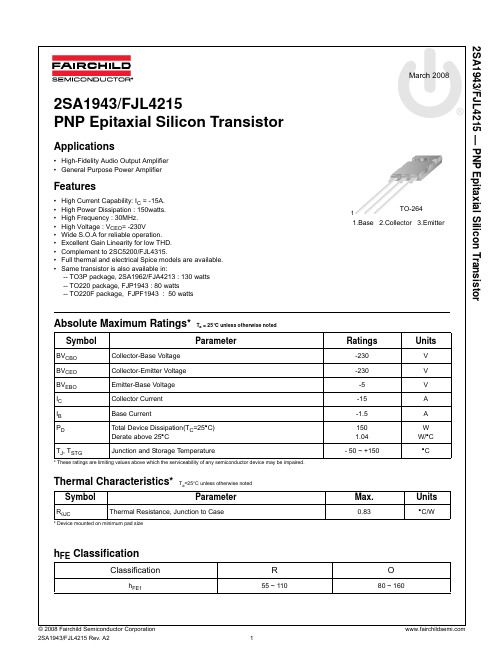
2SA1943/FJL4215 — PNP Epitaxial Silicon TransistorMarch 20082SA1943/FJL4215PNP Epitaxial Silicon TransistorApplications•High-Fidelity Audio Output Amplifier •General Purpose Power AmplifierFeatures•High Current Capability: I C = -15A.•High Power Dissipation : 150watts.•High Frequency : 30MHz.•High Voltage : V CEO = -230V•Wide S.O.A for reliable operation.•Excellent Gain Linearity for low THD.•Complement to 2SC5200/FJL4315.•Full thermal and electrical Spice models are available.•Same transistor is also available in:-- TO3P package, 2SA1962/FJA4213 : 130 watts -- TO220 package, FJP1943 : 80 watts -- TO220F package, FJPF1943 : 50 wattsAbsolute Maximum Ratings* T a= 25°C unless otherwise noted* These ratings are limiting values above which the serviceability of any semiconductor device may be impaired.Thermal Characteristics* T a=25°C unless otherwise noted* Device mounted on minimum pad sizeh FE ClassificationSymbolParameter RatingsUnitsBV CBO Collector-Base Voltage -230V BV CEO Collector-Emitter Voltage -230V BV EBO Emitter-Base Voltage -5V I C Collector Current -15A I B Base Current-1.5A P D Total Device Dissipation(T C =25°C)Derate above 25°C1501.04W W/°C T J , T STGJunction and Storage Temperature- 50 ~ +150°CSymbolParameterMax.UnitsR θJCThermal Resistance, Junction to Case0.83°C/WClassificationROh FE155 ~ 11080 ~ 1601.Base2.Collector3.Emitter1TO-2642SA1943/FJL4215 — PNP Epitaxial Silicon TransistorElectrical Characteristics* T a=25°C unless otherwise noted* Pulse Test: Pulse Width=20µs, Duty Cycle ≤2%Ordering InformationSymbolParameterTest ConditionMin.Typ.Max.UnitsBV CBO Collector-Base Breakdown Voltage I C =-5mA, I E =0-230V BV CEO Collector-Emitter Breakdown Voltage I C =-10mA, R BE =∞-230V BV EBO Emitter-Base Breakdown Voltage I E =-5mA, I C =0-5VI CBO Collector Cut-off Current V CB =-230V, I E =0-5.0µA I EBO Emitter Cut-off Current V EB =-5V, I C =0-5.0µAh FE1DC Current Gain V CE =-5V, I C =-1A 55160h FE2DC Current GainV CE =-5V, I C =-7A 3560V CE (sat)Collector-Emitter Saturation Voltage I C =-8A, I B =-0.8A -0.4-3.0V V BE (on)Base-Emitter On Voltage V CE =-5V, I C =-7A -1.0-1.5V f T Current Gain Bandwidth Product V CE =-5V, I C =-1A 30MHz C obOutput CapacitanceV CB =-10V, f=1MHz360pFPart NumberMarkingPackagePacking MethodRemarks2SA1943RTU A1943R TO-264TUBE hFE1 R grade 2SA1943OTU A1943O TO-264TUBE hFE1 O grade FJL4215RTU J4215R TO-264TUBE hFE1 R grade FJL4215OTUJ4215OTO-264TUBEhFE1 O grade2SA1943/FJL4215 — PNP Epitaxial Silicon Transistor2SA1943/FJL4215 PNP Epitaxial Silicon Transistor2SA1943/FJL4215Rev. I31TRADEMARKSThe following are registered and unregistered trademarks and service marks Fairchild Semiconductor owns or is authorized to use andis not intended to be an exhaustive list of all such trademarks.DISCLAIMERFAIRCHILD SEMICONDUCTOR RESERVES THE RIGHT TO MAKE CHANGES WITHOUT FURTHER NOTICE TO ANY PRODUCTS HEREIN TO IMPROVE RELIABILITY, FUNCTION, OR DESIGN. FAIRCHILD DOES NOT ASSUME ANY LIABILITY ARISING OUT OF THE APPLICATION OR USE OF ANY PRODUCT OR CIRCUIT DESCRIBED HEREIN; NEITHER DOES IT CONVEY ANY LICENSE UNDER ITS PATENT RIGHTS, NOR THE RIGHTS OF OTHERS. THESE SPECIFICATIONS DO NOT EXPAND THE TERMS OF FAIRCHILD’S WORLDWIDE TERMS AND CONDITIONS, SPECIFICALLY THE WARRANTY THEREIN, WHICH COVERS THESE PRODUCTS.LIFE SUPPORT POLICYFAIRCHILD’S PRODUCTS ARE NOT AUTHORIZED FOR USE AS CRITICAL COMPONENTS IN LIFE SUPPORT DEVICES OR SYSTEMS WITHOUT THE EXPRESS WRITTEN APPROVAL OF FAIRCHILD SEMICONDUCTOR CORPORATION.As used herein:1. Life support devices or systems are devices or systemswhich, (a) are intended for surgical implant into the body, or (b) support or sustain life, and (c) whose failure to perform when properly used in accordance with instructions for use provided in the labeling, can be reasonably expected to result in significant injury to the user.2.A critical component is any component of a life support device or system whose failure to perform can be reasonably expected to cause the failure of the life support device or system, or to affect its safety or effectiveness.PRODUCT STATUS DEFINITIONS Definition of Terms ACEx ®Build it Now™CorePLUS™CROSSVOLT ™CTL™Current Transfer Logic™EcoSPARK ®Fairchild ®Fairchild Semiconductor ®FACT Quiet Series™FACT ®FAST ®FastvCore™FPS™FRFET ®Global Power Resource SMGreen FPS™Green FPS™ e-Series™GTO™i-Lo ™IntelliMAX™ISOPLANAR™MegaBuck™MICROCOUPLER™MicroFET™MicroPak™MillerDrive™Motion-SPM™OPTOLOGIC ®OPTOPLANAR ®®PDP-SPM™Power220®Power247®POWEREDGE ®Power-SPM™PowerTrench ®Programmable Active Droop™QFET ®QS™QT Optoelectronics™Quiet Series™RapidConfigure™SMART START™SPM ®STEALTH™SuperFET™SuperSOT™-3SuperSOT™-6SuperSOT™-8SyncFET™The Power Franchise ®TinyBoost™TinyBuck™TinyLogic ®TINYOPTO™TinyPower™TinyPWM™TinyWire™µSerDes™UHC ®UniFET™VCX™Datasheet Identification Product Status DefinitionAdvance InformationFormative or In DesignThis datasheet contains the design specifications for product development. Specifications may change in any manner without notice.Preliminary First ProductionThis datasheet contains preliminary data; supplementary data will be pub-lished at a later date. Fairchild Semiconductor reserves the right to make changes at any time without notice to improve design.No Identification Needed Full ProductionThis datasheet contains final specifications. Fairchild Semiconductor reserves the right to make changes at any time without notice to improve design. Obsolete Not In ProductionThis datasheet contains specifications on a product that has been discontin-ued by Fairchild semiconductor. The datasheet is printed for reference infor-mation only.。
DSP4300系列数字式测试仪快速使用手册
1
DSP-LIA013
LIA013 适配器
1
CD-ROM LinkWare Software
电缆管理软件
1
User Manual Simplified Chinese
中文说明书
1
FLUKE corporation statement of calibration practices
FLUKE corporation statement of
calibration practices Case,soft
校准说明 软包
VERIFIED CONTENTS
P/N or FORM# N/A N/A
944223 658641 675611 944806 691623 642402 946769
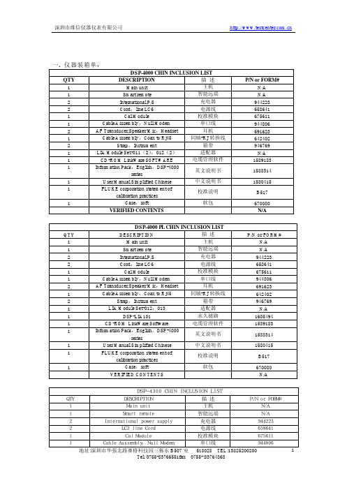
深圳市维信仪器仪表有限公司
DSP4000 数字式测试仪快速使用手册
一. 仪器装箱单:
QTY 1 1 2 2 1 1 2 1 2 1 1 1
1
DSP-4000 CHIN INCLUSION LIST
DESCRIPTION
描述
Main unit
主机
N/A 1605494 1589183
1588314
1580415
B517
670080 N/A
DSP-4300 CHIN INCLUSION LIST
QTY
DESCRIPTION
描 述
P/N or FORM#
1
Main unit
主机
N/A
1
Smart remote
智能远端
N/A
Smart remote
智能远端
MSK4300中文资料

ISD=10A, di/dt=100A/µS
-
MSK 4300H 3 Min. Typ. Max.
2.5
8
12.5
15
5.75 6.6
7.5
6.2
7.1
8.0
-
-
0.8
2.7
-
-
60
100 135
-1
-
+1
70
-
-
-
-
25
-
-
0.300
-
-
0.16
-
5
-
-
6
-
-
0.5
2
-
5
8
-
5
8
-
0.5
2
6.0
7.0
-
SWR Resistor=∞
4
SWR Resistor=∞
4
SWR Resistor=∞
4
SWR Resistor=∞
4
SWR =∞
4
Dead Time
SWR=12K
4
SOURCE-DRAIN DIODE CHARACTERISTICS
Байду номын сангаас
Forward Voltage
1
ISD=10A
-
Reverse Recovery Time 1
-
Low Level Input Current 1
VIN=0V
-
High Level Input Current 1
VIN=5V
-
OUTPUT BRIDGE
Drain-Source Breakdown Voltage 1 ID=25µA, All Inputs Off
- 1、下载文档前请自行甄别文档内容的完整性,平台不提供额外的编辑、内容补充、找答案等附加服务。
- 2、"仅部分预览"的文档,不可在线预览部分如存在完整性等问题,可反馈申请退款(可完整预览的文档不适用该条件!)。
- 3、如文档侵犯您的权益,请联系客服反馈,我们会尽快为您处理(人工客服工作时间:9:00-18:30)。
Collector-Emitter Voltage V C E (V)
Ambient Temperature Ta(˚C)
ቤተ መጻሕፍቲ ባይዱ98
Transient Thermal Resistance
125˚C
5
t s tg
1
–55˚C
Swi tchi ng T im e
0.5
1 0.5 t on 0.2 0.1 0.5
tf
10
5 0.02
0.05
0.1
0.5
1
5
1
5
0.1
1
10 Time t(ms)
100
3.0
1.2
1000
Collector Current I C (A)
5 (V CE =4V)
700mA
60 0m A
500m A
2
Collector Current I C (A)
300mA
3
200mA
Collector Current I C (A)
4
400 mA
4
3
mp)
Temp
)
e Te
(Cas
2
I B =100mA
1
2
Te m p) 25˚ C – 5 5 ˚C
元器件交易网
2SC4300
Silicon NPN Triple Diffused Planar Transistor (High Voltage Switchihg Transistor) sAbsolute maximum ratings (Ta=25°C)
Symbol VCBO VCEO VEBO IC IB PC Tj Tstg 2SC4300 900 800 7 5(Pulse10) 2.5 75(Tc=25°C) 150 –55 to +150 Unit V V V A A W °C °C
Symbol ICBO IEBO V(BR)CEO hFE VCE(sat) VBE(sat) fT COB Conditions VCB=800V VEB=7V IC=10mA VCE=4V, IC=2A IC=2A, IB=0.4A IC=2A, IB=0.4A VCE=12V, IE=–0.5A VCB=10V, f=1MHz
Application : Switching Regulator and General Purpose
(Ta=25°C) 2SC4300 100max 100max 800min 10 to 30 0.5max 1.2max 6typ 75typ V V
16.2
sElectrical Characteristics
3.35
1.5
B
C
E
Weight : Approx 6.5g a. Type No. b. Lot No.
I C – V CE Characteristics (Typical)
5
V CE (sat),V BE (sat) – I C Temperature Characteristics (Typical)
Collector Current I C (A)
Safe Operating Area (Single Pulse)
20 10 5 Collector Curre nt I C ( A)
10
10 µs
Reverse Bias Safe Operating Area
20 10 80
P c – T a Derating
Collector-Emitter Saturation Voltage V C E (s at) (V ) Base-Emitter Saturation Voltage V B E (s at) (V) (I C /I B =5)
I C – V BE Temperature Characteristics (Typical)
1
1
V C E (sat) 0 0.03 0.05 0.1 0.5
C 125˚C (
as
e
0
0
1
2
3
4
1
5
10
0
0
0.2
0.4
0.6
0.8
–55˚C (C
–55˚C (Case Temp) 25˚C (Case Temp) e Temp) 125˚C (Cas
125˚C
25˚C
(Case
V B E (sat)
External Dimensions FM100(TO3PF)
0.8±0.2 15.6±0.2 5.5±0.2 3.45 ±0.2 5.5 ø3.3±0.2 1.6
Unit
µA
23.0±0.3
V
9.5±0.2
µA
a b
MHz pF
1.75 2.15 1.05 +0.2 -0.1 5.45±0.1 5.45±0.1 4.4 1.5 0.65 +0.2 -0.1
3.3
0.8
sTypical Switching Characteristics (Common Emitter)
VCC (V) 250 RL (Ω) 125 IC (A) 2 VBB1 (V) 10 VBB2 (V) –5 IB1 (A) 0.3 IB2 (A) –1 ton (µs) 1max tstg (µs) 5max tf (µs) 1max
t on• t s t g • t f (µ s)
t on •t stg • t f – I C Characteristics (Typical)
θ j-a – t Characteristics
2
DC Cur rent Gain h F E
25˚C
VCC 250V IC:IB1:–IB2 =2:0.3:1 Const.
ase Tem
p)
1.0
Collector-Emitter Voltage V C E (V)
Collector Current I C (A)
Base-Emittor Voltage V B E (V)
(V C E =4V) 50 10
θ j- a ( ˚C/W)
h FE – I C Characteristics (Typical)
Without Heatsink Natural Cooling L=3mH IB2=–1.0A Duty:less than 1%
20
0.01
10
50
100
500
1000
0.01 50
100
500
1000
3.5 0
Without Heatsink 0 50 100 150
Collector-Emitter Voltage V C E (V)
1m
0µ
s
s
5 Collector Curr ent I C (A)
M aximum Power Dissipa ti on P C (W)
60
W ith In
1 0.5
fin
1 0.5
ite he
40
at si nk
0.1 0.05
Without Heatsink Natural Cooling
0.1 0.05