Cadence_Menu cadence软件菜单中英文对照图
Cadence-Menu--cadence软件菜单中英文对照图
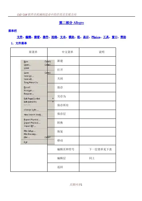
第二部分Allegro菜单栏文件、编辑、察看、器件、连线、文本、模块、组、显示、PSpice、工具、窗口、帮助1.文件菜单原菜单中文菜单说明新建打开关闭保存另存为保存所有保存层转换恢复移动编辑页和符号下一层菜单见下表编辑层同上返回改变组件设置启动的工具察看搜索栈物理输出进行封装并输出物理输入从Allegro导入IFF输入导入IFF文件打印设置打印预览打印输出可输出原理图退出注:若菜单中的说明项为空,则表示不不需要说明或说明项与中文菜单相似。
以下相同。
下一页前一页转向加入新页下一层上一层2.编辑菜单撤销重做移动复制复制所有重复复制排列删除颜色分割镜像翻转旋转模块顺序画弧画圆3.察看菜单放大矩形范围放大到满屏放大缩小按比例放大上移下移左移右移预览网格设定状态条错误信息条控制窗口数据栏工具栏4.器件菜单添加器件替换器件改变版本可改变器件符号的显示类型修改部分可设置器件在封装中的位置交换针脚删除5.连线菜单连线需要从一点画到另一点连线点击两点自动连线添加信号名添加总线名连结总线设定总线参数画点连线加粗连线减细设置连线的图案6.文本菜单特性设置习惯设置器件赋值可对电阻电容等进行赋值理性文本设置端点的名称添加注释打开文本文档设置字体大小放大缩小交换重新连结特性显示下一层菜单如下显示名称显示值两样都显示不可见7.模块菜单添加重命名扩展连线连线添加针脚重命名针删除针脚移动针脚输入针脚输出针脚双向针脚8.组菜单创建组下一层菜单在下表设定当前组显示组的内容移动复制复制全部设置复制个数设置文字大小改变注释删除设定颜色激活器件特性显示矩形框内创建为一组多边形框内创建为一组用表达式创建下一个在组中去除一个器件在组中添加一个器件替换改变显示版本删除修改显示名称显示值两样都显示不可见9.显示菜单激活去激活联系显示信号名和文本与器件的连结关系颜色器件信息连结显示点的坐点击一点标显示目录显示距离点击两点,在下方状态栏显示显示历史信息设置快捷键显示修改信息显示线网信点击线网息显示端点针脚显示所有的针脚针脚名显示点击的器件的针脚名显示特性显示所有器件的针脚信息返回显示字体尺在下方状态栏显示寸10.Pspice菜单创建仿真文件编辑仿真文件删除仿真文件检查生成网表查看网表运行查看结果编辑模型编辑激励仿真多重文件模拟数据11.工具菜单扩展设计取消扩展当前编辑全局查找查找某一个器件全局导航可查出某个器件属于哪个库限制管理器检查进行错误检查显示错误显示错误及告警信息运行script文件反标将封装后的信息标注在原理图仿真层次编辑生成符号图可用于层次设计封装应用程序下一层菜单如下表设计差别比较可将原理图的修改更新到板子设计联系习惯设置可编辑设计环境、快捷键等选项可设置栅格尺寸等材料清单电气规则检查生成网表报告12.窗口菜单新开一个窗口刷新层叠将多个窗口层叠摆放平铺将多个窗口平铺展开排列图标当前激活的窗口13.帮助菜单帮助主题新增功能主要帮助常见问题及解决方法产品说明Cadence文件可链接到Cadence公司网站关于Concept-HDL显示版本信息第二部分Allegro菜单栏文件、编辑、察看、添加、显示、设置、逻辑、布局、布线、分析、制造、工具、帮助1.文件菜单新建打开保存另存为导入导出查看日志打开日志打印设置打印改变编辑器生成说明文件退出2.编辑菜单移动复制镜像旋转修改删除生成图形删除未连结的图形分割平面倒角修改器件边角删除倒角文本分组特性设定3.查看菜单放大矩形范围放大至满屏放大缩小放大整个范围以一点为中心放大保存镜像文件镜像文件恢复刷新习惯设置4.添加菜单线弧形3点弧形圆四边形填充的四边形文本图形实心填充不填充交叉线网填充5.显示菜单颜色设置显示颜色面板元件信息测量寄生参数特性设置激活去激活显示飞线不显示飞线6.设置菜单画图尺寸画图选择文字大小网格设置子目录层结构过孔设置限制设置电气规则设定特性定义线网定义区域内可放置封装区域内不可放置封装区封装高度区域内可布线区域内不可布线区域内不可设置过孔区域内不可设置探针区域内不可优化布线影像输出外框7.逻辑菜单线网逻辑线网方案设置差分对标识直流线网设置RefDes自动命名RefDes改变器件终端设定重命名重命名整个设计重命名一个区域内元件重命名窗口内元件重命名列表中的元件8.布局菜单手工布局快速放置在CCT中布局自动布局交互式布局交换自动交换调整更新符号临时使用SPECCTRAQuest交换针脚交换功能交换元件可视布局参数设定布局布顶层元件布底层元件布设计中的元件布指定区域的元件布窗口中的元件布列表中的元件参数设定交换设计内容交换指定区域交换窗口内容交换列表内容参数设定调整整个设计调整指定区域调整窗口中内容调整列表内容器件符号9.布线菜单连线倒角光滑边角在CCT中布线优化测试准备运行布线检查选择式布线自动布线交互编辑参数设定优化设计优化指定区域优化窗口优化激活内容优化列表内容自动设置生成测试点删除测试点交换测试点测试记录10.分析菜单初始化选择库信号完整选择模型 去除模型 参数设定 审查 检测 串扰设置初始化自动设置手工设置 规则选择规则审查 规则执行 运行结果 审查报告 执行报告11.制造菜单图样设置影像文件设定电磁干扰文件输出钻孔参数设定设置标识制造检查设置测试内容丝印层设置生成报告钻孔参数钻孔图例钻孔记录文件输出生成组装图生成材料清单参数设置设置字体类型测直线距离测角度生成详细说明13.工具菜单创建模块焊盘编辑可进行有关焊盘的操作焊盘去除连结报告技术文件比较设置向导数据库检查更新DRC DRC为设计规则检查修改设计焊盘修改焊盘库替换焊盘组编辑刷新修改边界恢复恢复所有14.帮助菜单帮助内容设计流程产品说明常见问题及其解答网络链接Allegro文档可链接到Cadence网站关于Allegro专家显示版本信息等。
CAD中英文对照
bump map凹凸贴图凸纹贴图
button menu按钮菜单按钮功能表
BYBLOCK随块BYBLOCK
BYLAYER随层BYLAYER
byte字节位元组
cabling电缆布线配线
cal计算器校正
calibrate校准校正
call调用呼叫
callback回调(for LISP)回覆
autocommit自动提交自动确定
AutoTrack自动追踪自动追踪
axis tripod三轴架三向轴
azimuth方位角方位
Back Clipping On后向剪裁打开
back view后视图后视景
background color背景色背景颜色
backup备份备份
Backward反向左右反向
bad不正确的不正确
bitmap位图点阵图
blend合成混成
blipmode点标记模式点记模式
block块图块
block definition块定义图块定义
block reference块参照图块参考
block table块表图块表格
bmpout BMP输出BMP汇出
body体主体
Boolean operation布尔运算布林运算
digitizing puck数字化仪游标数位化指向器
dim标注标注
dimaligned对齐标注对齐式标注
dimangular角度标注角度标注
dimbaseline标注基线基线式标注
dimcenter圆心标注中心点标注
dimcontinue连续标注连续式标注
dimdiameter直径标注直径标注
dimedit标注编辑标注编辑
CAD中英文对照表
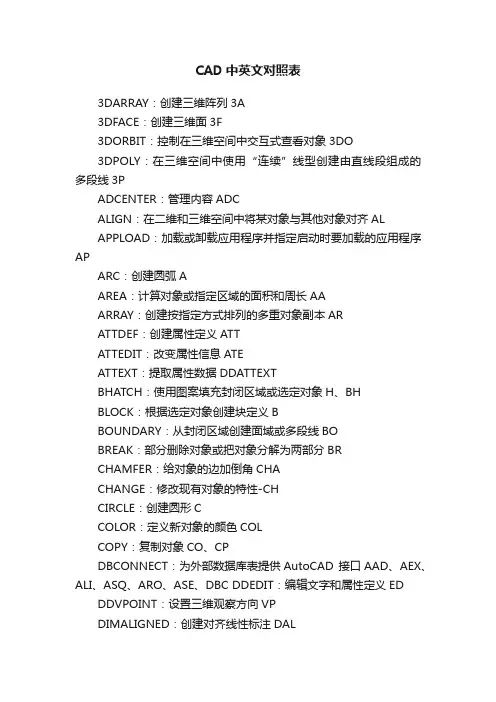
CAD中英文对照表3DARRAY:创建三维阵列3A3DFACE:创建三维面3F3DORBIT:控制在三维空间中交互式查看对象3DO3DPOLY:在三维空间中使用“连续”线型创建由直线段组成的多段线3PADCENTER:管理内容ADCALIGN:在二维和三维空间中将某对象与其他对象对齐ALAPPLOAD:加载或卸载应用程序并指定启动时要加载的应用程序APARC:创建圆弧AAREA:计算对象或指定区域的面积和周长AAARRAY:创建按指定方式排列的多重对象副本ARATTDEF:创建属性定义ATTATTEDIT:改变属性信息ATEATTEXT:提取属性数据DDATTEXTBHATCH:使用图案填充封闭区域或选定对象H、BHBLOCK:根据选定对象创建块定义BBOUNDARY:从封闭区域创建面域或多段线BOBREAK:部分删除对象或把对象分解为两部分BRCHAMFER:给对象的边加倒角CHACHANGE:修改现有对象的特性-CHCIRCLE:创建圆形CCOLOR:定义新对象的颜色COLCOPY:复制对象CO、CPDBCONNECT:为外部数据库表提供AutoCAD 接口AAD、AEX、ALI、ASQ、ARO、ASE、DBC DDEDIT:编辑文字和属性定义ED DDVPOINT:设置三维观察方向VPDIMALIGNED:创建对齐线性标注DALDIMANGULAR:创建角度标注DANDIMBASELINE:从上一个或选定标注的基线处创建线性、角度或坐标标注DBA DIMCENTER:创建圆和圆弧的圆心标记或中心线DCE DIMCONTINUE:从上一个或选定标注的第二尺寸界线处创建线性、角度或坐标标注DCO DIMDIAMETER:创建圆和圆弧的直径标注DDIDIMEDIT:编辑标注DEDDIMLINEAR:创建线性尺寸标注DLIDIMORDINATE:创建坐标点标注DORDIMOVERRIDE:替代标注系统变量DOVDIMRADIUS:创建圆和圆弧的半径标注DRADIMSTYLE:创建或修改标注样式DDIMTEDIT:移动和旋转标注文字DIMTEDDIST:测量两点之间的距离和角度DIDIVIDE:将点对象或块沿对象的长度或周长等间隔排列DIVDONUT:绘制填充的圆和环DODRAWORDER:修改图像和其他对象的显示顺序DRDSETTINGS:指定捕捉模式、栅格、极坐标和对象捕捉追踪的设置DS、RM、SE DSVIEWER:打开“鸟瞰视图”窗口AV DVIEW:定义平行投影或透视视图DVELLIPSE:创建椭圆或椭圆弧ELERASE:从图形中删除对象EEXPLODE:将组合对象分解为对象组件XEXPORT:以其他文件格式保存对象EXPEXTEND:延伸对象到另一对象EXEXTRUDE:通过拉伸现有二维对象来创建三维原型 EXTFILLET:给对象的边加圆角FFILTER:创建可重复使用的过滤器以便根据特性选择对象FIGROUP:创建对象的命名选择集GHATCH:用图案填充一块指定边界的区域-HHATCHEDIT:修改现有的图案填充对象HEHIDE:重生成三维模型时不显示隐藏线HIIMAGE:管理图像IMIMAGEADJUST:控制选定图像的亮度、对比度和褪色度IADIMAGEATTACH:向当前图形中附着新的图像对象IATIMAGECLIP:为图像对象创建新剪裁边界ICLIMPORT:向AutoCAD 输入文件IMPINSERT:将命名块或图形插入到当前图形中IINTERFERE:用两个或多个三维实体的公用部分创建三维复合实体INFINTERSECT:用两个或多个实体或面域的交集创建复合实体或面域并删除交集以外的部分IN INSERTOBJ:插入链接或嵌入对象IO LAYER:管理图层和图层特性LA-LAYOUT:创建新布局,重命名、复制、保存或删除现有布局LO LEADER:创建一条引线将注释与一个几何特征相连 LEADLENGTHEN:拉长对象LENLINE:创建直线段LLINETYPE:创建、加载和设置线型LTLIST:显示选定对象的数据库信息LI、LSLTSCALE:设置线型比例因子LTSLWEIGHT:LWMATCHPROP:设置当前线宽、线宽显示选项和线宽单位MAMEASURE:将点对象或块按指定的间距放置MEMIRROR:创建对象的镜像副本MIMLINE:创建多重平行线MLMOVE:在指定方向上按指定距离移动对象MMSPACE:从图纸空间切换到模型空间视口MSMTEXT:创建多行文字T、MTMVIEW:创建浮动视口和打开现有的浮动视口MVOFFSET:创建同心圆、平行线和平行曲线OOPTIONS:自定义AutoCAD 设置GR、OP、PROSNAP:设置对象捕捉模式OSPAN:移动当前视口中显示的图形PPASTESPEC:插入剪贴板数据并控制数据格式PAPEDIT:编辑多段线和三维多边形网格PEPLINE:创建二维多段线PLPRINT :将图形打印到打印设备或文件PLOTPOINT:创建点对象POPOLYGON:创建闭合的等边多段线POLPREVIEW:显示打印图形的效果PREPROPERTIES:控制现有对象的特性CH、MO PROPERTIESCLOSE:关闭“特性”窗口PRCLOSEPSPACE:从模型空间视口切换到图纸空间PSPURGE:删除图形数据库中没有使用的命名对象,例如块或图层PU QLEADER:快速创建引线和引线注释LEQUIT:退出AutoCAD EXITRECTANG:绘制矩形多段线RECREDRAW:刷新显示当前视口RREDRAWALL:刷新显示所有视口RAREGEN:重生成图形并刷新显示当前视口REREGENALL:重新生成图形并刷新所有视口REAREGION:从现有对象的选择集中创建面域对象REGRENAME:修改对象名RENRENDER:创建三维线框或实体模型的具有真实感的渲染图像RR REVOLVE:绕轴旋转二维对象以创建实体REVRPREF:设置渲染系统配置RPRROTATE:绕基点移动对象ROSCALE:在X、Y 和Z 方向等比例放大或缩小对象 SCSCRIPT:用脚本文件执行一系列命令SCRSECTION:用剖切平面和实体截交创建面域SECSETVAR:列出系统变量并修改变量值SETSLICE:用平面剖切一组实体SLSNAP:规定光标按指定的间距移动SNSOLID:创建二维填充多边形SOSPELL:检查图形中文字的拼写SPSPLINE:创建二次或三次(NURBS) 样条曲线SPLSPLINEDIT:编辑样条曲线对象SPESTRETCH:移动或拉伸对象SSTYLE:创建或修改已命名的文字样式以及设置图形中文字的当前样式ST SUBTRACT:用差集创建组合面域或实体SUTABLET:校准、配置、打开和关闭已安装的数字化仪TA THICKNESS:设置当前三维实体的厚度THTILEMODE:使“模型”选项卡或最后一个布局选项卡当前化TI、TM TOLERANCE:创建形位公差标注TOLTOOLBAR:显示、隐藏和自定义工具栏TOTORUS:创建圆环形实体 TORTRIM:用其他对象定义的剪切边修剪对象TRUNION:通过并运算创建组合面域或实体UNIUNITS:设置坐标和角度的显示格式和精度UNVIEW:保存和恢复已命名的视图VVPOINT:设置图形的三维直观图的查看方向-VPWBLOCK:将块对象写入新图形文件WWEDGE:创建三维实体使其倾斜面尖端沿X 轴正向WE XATTACH:将外部参照附着到当前图形中XAXBIND:将外部参照依赖符号绑定到图形中XBXCLIP:定义外部参照或块剪裁边界,并且设置前剪裁面和后剪裁面XC XLINE:创建无限长的直线(即参照线)XLXREF:控制图形中的外部参照XRZOOM:放大或缩小当前视口对象的外观尺寸ZAUTO CAD快捷键常见命令(一)字母类1、对象特性ADC, *ADCENTER(设计中心“Ctrl+2”)CH, MO *PROPERTIES(修改特性“Ctrl+1”)MA, *MATCHPROP(属性匹配)ST, *STYLE(文字样式)COL, *COLOR(设置颜色)LA, *LAYER(图层****作)LT, *LINETYPE(线形)LTS, *LTSCALE(线形比例)LW, *LWEIGHT (线宽)UN, *UNITS(图形单位)ATT, *ATTDEF(属性定义)ATE, *ATTEDIT(编辑属性)BO, *BOUNDARY(边界创建,包括创建闭合多段线和面域)AL, *ALIGN(对齐)EXIT, *QUIT(退出)EXP, *EXPORT(输出其它格式文件)IMP, *IMPORT(输入文件)OP,PR *OPTIONS(自定义CAD设置)PRINT, *PLOT(打印)PU, *PURGE(清除**)R, *REDRAW(重新生成)REN, *RENAME(重命名)SN, *SNAP(捕捉栅格)DS, *DSETTINGS(设置极轴追踪)OS, *OSNAP(设置捕捉模式)PRE, *PREVIEW(打印预览)TO, *TOOLBAR(工具栏)V, *VIEW(命名视图)AA, *AREA(面积)DI, *DIST(距离)LI, *LIST(显示图形数据信息)2、AUTO CAD快捷绘图命令:PO, *POINT(点)L, *LINE(直线)XL, *XLINE(射线)PL, *PLINE(多段线)ML, *MLINE(多线)SPL, *SPLINE(样条曲线)POL, *POLYGON(正多边形)REC, *RECTANGLE(矩形)C, *CIRCLE(圆)A, *ARC(圆弧)DO, *DONUT(圆环)EL, *ELLIPSE(椭圆)REG, *REGION(面域)MT, *MTEXT(多行文本)T, *MTEXT(多行文本)B, *BLOCK(块定义)I, *INSERT(插入块)W, *WBLOCK(定义块文件)DIV, *DIVIDE(等分)H, *BHATCH(填充)3、AUTO CAD快捷修改命令:CO, *COPY(复制)MI, *MIRROR(镜像)AR, *ARRAY(阵列)O, *OFFSET(偏移)RO, *ROTATE(旋转)M, *MOVE(移动)E, DEL键*ERASE(删除)X, *EXPLODE(分解)TR, *TRIM(修剪)EX, *EXTEND(延伸)S, *STRETCH(拉伸)LEN, *LENGTHEN(直线拉长)SC, *SCALE(比例缩放)BR,*BREAK(打断)CHA, *CHAMFER(倒角)F, *FILLET(倒圆角)PE, *PEDIT(多段线编辑)ED, *DDEDIT(修改文本)4、AUTO CAD快捷视窗缩放:P, *PAN(平移)Z+空格+空格, *实时缩放Z, *局部放大Z+P, *返回上一视图Z+E, *显示全图5、AUTO CAD快捷尺寸标注:DLI, *DIMLINEAR(直线标注)DAL, *DIMALIGNED(对齐标注)DRA, *DIMRADIUS(半径标注)DDI, *DIMDIAMETER(直径标注)DAN, *DIMANGULAR(角度标注)DCE, *DIMCENTER(中心标注)DOR, *DIMORDINATE(点标注)TOL, *TOLERANCE(标注形位公差)LE, *QLEADER(快速引出标注)DBA, *DIMBASELINE(基线标注)DCO, *DIMCONTINUE(连续标注)D, *DIMSTYLE(标注样式)DED, *DIMEDIT(编辑标注)DOV, *DIMOVERRIDE(替换标注系统变量)(二)AUTO CAD快捷常用CTRL快捷键【CTRL】+1 *PROPERTIES(修改特性) 【CTRL】+2 *ADCENTER(设计中心)【CTRL】+O *OPEN(打开文件)【CTRL】+N、M *NEW(新建文件)【CTRL】+P *PRINT(打印文件)【CTRL】+S *SAVE(保存文件)【CTRL】+Z *UNDO(放弃)【CTRL】+X *CUTCLIP(剪切)【CTRL】+C *COPYCLIP(复制)【CTRL】+V *PASTECLIP(粘贴)【CTRL】+B *SNAP(栅格捕捉)【CTRL】+F *OSNAP(对象捕捉)【CTRL】+G *GRID(栅格)【CTRL】+L *ORTHO(正交)【CTRL】+W *(对象追踪)【CTRL】+U *(极轴)(三)AUTO CAD快捷常用功能键【F1】*HELP(帮助)【F2】*(文本窗口)【F3】*OSNAP(对象捕捉)【F7】*GRIP(栅格)【F8】*ORTHO(正交。
Cadence 手册详细图解 英文版
Cadence IC Design ManualFor EE5518ZHENG Huan QunLin Long YangRevised onMay 2017Department of Electrical & Computer EngineeringNational University of SingaporeContents1 INTRODUCTION (4)1.1 Overview of Design Flow (4)1.2 Getting Started with Cadence (6)1.3 Using Online Help (8)1.4 Exit Cadence (8)2 SCHEMATIC ENTRY (9)2.1 Creating a New Design Library (9)2.2 Creating a Schematic Cellview (10)2.3 Adding Components to Schematic (11)2.4 Adding Pins to Schematic (12)2.5 Adding Wires to Schematic (13)2.6 Saving Your Design (14)3 SYMBOL AND TEST CIRCUIT CREATION (15)3.1 Creating Symbol (15)3.2 Editing Symbol (16)3.3 Building Test Bench (18)4 SIMULATING YOUR CIRCUIT (21)4.1 Start the Simulation Environment (21)4.2 Selecting Project Directory (21)4.3 Setup Model Library (22)4.4 Choosing the Desired Analysis (22)4.5 Setup Variables (23)4.6 Saving Simulation Data (24)4.7 Saving Output for Plotting (24)4.8 Viewing the Netlists (25)4.9 Running the Simulation (25)5 PHYSICAL LAYOUT (28)5.1 Layout vs Symbol of CMOS Devices (28)5.2 Starting Layout Editor (29)5.3 Vias (31)5.4 Changing the Grid (33)5.5 Inserting and Editing Instances (34)5.6 Drawing Shapes / Paths (35)5.7 Creating Pins (36)6 DESIGN VERIFICATION: DRC AND LVS (38)6.1 Performing DRC (38)6.2 Performing LVS (40)6.3 Performing PEX (41)7 POST‐LAYOUT SIMULATION (45)7.1 Simulation the Extracted Cell View (45)8 CONCLUSION (46)1INTRODUCTIONThis manual describes how to use Cadence IC design tools. It covers the whole design cycle, from the front-end to the back-end, i.e., from the pre-layout design to the post-layout design.The manual aims to provide a guide for fresh users. Following the manual, users can start doing analog IC design even though the users don’t have any knowledge of the tools.An inverter is used to illustrate the whole cycle of analog IC design, and Cadence Generic 45nm (cg45nm) kit is the technology library used for implementing the inverter. The method stated in the manual can be applied to other type of analog circuit design.1.1Overview of Design FlowFigure 1 shows a typical analog IC design flow.The design flow starts from schematic entry with the Cadence schematic capture tool –Schematic Editor. Devices or cells from the cg45nm or other libraries are used to build your circuit. Your design is hierarchical; therefore higher level schematics also incorporate cells which you have already developed. The schematics which you enter at this stage therefore typically consist of a number of base library cells and also lower level cells designed yourself.These are described in Sections 2 and 3 of the manual.When you have finished designing a particular circuit, you need to simulate it to ensure that it works as expected. It would be unlikely that your circuit works as expected at the first time so you have to repeat the cycle to improve the circuit, as shown in Figure 1, until the circuit works satisfactorily. This must be done for each sub-circuit of your design and then for the top level design. How to simulate and view the performance of simulation results are presented in Sections 4 of the manual.When the performance of the circuit is satisfactory, it is ready to start the physical design or layout of the circuit. The layout starts with the cell or device placement. Once the cells have been placed, routing can be carried out. Routing connects the cells/device of the design.After finishing placement and routing, the layout has to go through the Design Rule Check (DRC) with rule decks provided by PDK provider, to ensure that there is no design rule violation in the layout. The layout has to be rectified accordingly to the rules’ requirement till it passes DRC.Upon a successful DRC, it is Layout-versus-Schematic (LVS) check, to assure that all connections in the layout are correct. The layout has to be amended accordingly to the schematic If LVS doesn’t pass. DRC has to be done whenever layout is changed. The process is repeated until the LVS passes.Figure 1. Analog IC Design FlowThe next step is parasitic extraction (PEX) to get the extracted view of the circuit, which is used for post–layout simulation. The extracted view includes the parasitic effects in both the instances/devices and the required wiring interconnects of the circuit.Following DRC, LVS and PEX, it is post-layout simulation. The post-layout simulation is essential to make sure that the circuit with the extra parasitic parameters functions well and still meet the design specifications. If the performance of the post-layout simulation is not acceptable, back to the stage of schematic entry to check the circuit. Basically, re-design the circuit is necessary. Repeat the whole flow until the results of the post-layout simulation meet the design specifications.If everything is satisfactory, the next stage is GDSII Generation. It generates a file which depicts the low level geometry of layout. GDSII format is industry standard format suitable fora semiconductor company to fabricate and manufacture the chip of layout. This is briefed inthe last section of the manual.1.2Getting Started with CadenceUpon logging into your account, you will be brought to the Linux Desktop Environment.Right click on the desktop and click Open Terminal to open a “window” on the desktop. This window is the Linux command line prompt at which you can run Linux commands. After running a Linux command, this window also shows the output of the command.The following steps show how to start Cadence with cg45nm kit.A.Create a working directory - project (it can be any name as you like) with thecommand:mkdir projectwhere mkdir is Linux command and the project is the directory name;B.Enter the working directory with the command:cd projectwhere the cd is the Linux command;C.Type the followings commands to do the environment setup for using Cadence Generic45nm PDK.cp /app11/cg45nm/USERS/cds.lib .cp /app11/cg45nm/USERS/assura_tech.lib .cp /app11/cg45nm/USERS/pvtech.lib .D.Start cadence in the working directory – project with the following command:virtuoso &where virtuoso is the command to start Cadence IC design tool.Now, Cadence tools are successfully started. Keeps only the Command Input Window (CIW) which is shown in Figure 2.Figure 2. CIW WindowDo not close this CIW and try to keep it in view whenever you are using Cadence. Error messages and output from some of the tools are always sent to the CIW. If something doesn't appear to be working, always check the CIW for error messages. In addition, the CIW allows the user great control over Cadence by interpreting skill commands which are typed into it.E.In the CIW, select Tools Library Manager. The Library Manager pop up as inFigure 3. The Library Manager is where you create, add, copy, delete and organizeyour libraries and cell views.Figure 3. Library Manager WindowYou can see that the library gpdk045 appears in the Library column of the librarymanager.Now, you have started Cadence tool and loaded the cg45nm kit successfully. There are some documents in /app11/cg45nm/ gpdk045_v4_0/docs, and you can always refer to these documents for the information such as devices, device models, DRC rules and others related to cg45nm kit.Next time, you need only to repeat the steps B and D, for launching Cadence virtuoso and doing your project.1.3Using Online HelpCadence provides a comprehensive online manuals for all Cadence tools. You can launch the online help by typing the following command at the Linux prompt.cdnshelpThis invokes the online software manuals. Alternately, there is a help menu on each Cadence window. Manual which is related to that window related will pop-up once clicking on the help button.1.4Exit CadenceTo exit Cadence, just click on the cross sign X or File Exit in CIW. It is necessary to exit Cadence when it is not in use. Your library file would be locked or cannot edited next time if Cadence was not exited properly.2SCHEMATIC ENTRYNow that Cadence is running, you are almost ready to start entering schematics. However, you must first create a library which will be used to store all the parts of your design. Then, schematic can be created in the library.2.1Creating a New Design LibraryA.In the Library Manager window, select File→New→Library. New Library formpops up as shown in Figure 4.B.In the New Library form referring to Figure 4, key in your design library name(example: test) in the field of Name, and then click Ok.C.Click Ok in the pop-up window - the Technology File for New Library, referring toFigure 5.D.Choose gpdk045 in the Attach Library to Technology Library form, referring toFigure 6, and then click Ok.Figure 4. New Library FormFigure 5. Technology File for New Library FormFigure 6. Attach Library to Technology File FormA new library, named test, should appear in your Library Manager window.2.2 Creating a Schematic CellviewA.In Library Manager, select the Library where you would like to create a schematic. Then,select File→New→Cell View.B.Set up the New File form as Figure 7Figure 7. Create CellViewC.Click OK when done. A blank schematic window for the "inv" (your cell name)schematic appears.Explore the functions available by putting your mouse over the toolbar and fixed menu icons.In addition, note that some of the menu selections have alphabets listed to the right of them. These are bind-key or shortcut-key definitions which are very useful in the long run.Test them out during the schematic drawing in subsequent steps.2.3Adding Components to SchematicFigure 8 shows the schematic which you are going to patch, and the property of each component is listed in Table 1.Figure 8. Inverter CircuitTabel 1. Component Properties of Figure 8: Inverter CircuitComponents Library Name Cell Name PropertiesPMOS gpdk045 pmos1v l:45nm w:120nm (default size)NMOS gpdk045 nmos1v l:45nm w:120nm (default size)Here is the example on how to add component instances by placing cell views from libraries. Type “i” bind-key or select Create Instance in the schematic window or click on the menu bar to display Add Instance form. Then in the Add Instance window, select gpdk045as Library, choose the NMOS transistor by selecting nmos1v in Cell and also choose symbol as View, as shown in Figure 9.Figure 9. Add Instance FormSimilarly, add the pmos1v into the schematic. As an example, here we just keep all theparameters as default.If you place a component with the wrong parameter values, select the component and type “q” bindkey or use the Edit→Properties→Objects command to change the parameters. Use the Edit→Move command or type “m” if you place components in the wrong location.2.4Adding Pins to SchematicYou must place I/O pins in your schematic to identify the inputs and the outputs. A pin can be an input, output or an input-output (bi-directional) pin.Type “p” or select Add →Pin from inv Schematic Window or click the Pin fixed menuicon in the schematic window. The Add Pin form appears as Figure 10.Figure 10. Add Pin FormClick Hide and move you cursor to the Schematic Window. Place pins at the correct places and click right mouse key to rotate the pin if necessary.Add pins according to Table 2, paying attention to the direction.Table 2. Pin Names and Direction of invPin Names DirectionVin InputVout OutputVDD, GND Input-OutputCaution: Do not use the add component form to place schematic pins.2.5 Adding Wires to SchematicAdd wires to connect the components and pins in the design.A.Type “w” or select Add →Wire (narrow) in Schematic Window or click (narrow)fixed menu icon.B.In the schematic window, click on a pin of one of your components as the first pointfor your wiring. A diamond shape appears over the starting point of this wire.C.Follow the prompts at the bottom of the design window and click left mouse key onthe destination point for your wire.D.Continue wiring the schematic. When done wiring, press Esc with your cursor in theschematic window to cancel wiring.2.6Saving Your DesignCheck the design to ensure that it is correct and save the design.A.Click the Check and Save icon in the schematic window.B.Observe the CIW output area, for the information of the check and save action.3SYMBOL AND TEST CIRCUIT CREATIONSymbols are useful when creating designs as it is impractical to show every transistor on the top level schematic. Instead, the symbols of cells are created in order to instantiate them in the higher level schematics and make them more readable (i.e. hierarchical designs). Create a symbol for your design so you can place it in a test circuit for simulation.3.1Creating SymbolA.In the inv schematic window, select Create → Cellview → From Cellview. CellviewFrom Cellview pops up as shown in Figure 11.Figure 11. Cellview From Cellview FormB.Click OK in the Cellview From Cellview form. The Symbol Generation Options formappears as Figure 12. Enter the information listed in Table 3 for the symbol.Table 3: Pin SpectificationsLeft Pins : VinRight Pins : VoutTop Pins: VDDBottom Pins: GNDFigure 12. Symbol Generation Options FormC.Click OK in the Symbol Generation Options form. A window with a symbol createdautomatically by the tools pops up, referring to Figure 13.Figure 13. Symbol Generated AutomaticallyD.Observe the CIW output pane and note the messages stating Adding ‘CDFinformation ...’.3.2Editing SymbolYou can modify the symbol to have a more meaningful shape for easy recognition.A.Move your cursor over the symbol, until the entire green rectangle is highlighted. Clickleft to select it.B.Click Delete icon in the symbol window to delete the green rectangle.C.Select Create→Shape→Polygon. Follow the prompts at the bottom of the symbol, anddraw the triangle shown in Figure 14.D.Type “m” or click Move icon in the symbol window, move the pins to the finaldestination.E.Select [@partName], and use Edit→Properties→Object to change it to inverter asshown in Figure 14.Figure 14. Edit Object Properties FormF.Save your edited symbol view. The final symbol is shown in Figure 15.Figure 15. Symbol of inv3.3Building Test BenchTo test the inverter that you have just built, you need to create a test bench. This test bench will also be used during the post-layout simulation.Creating an inv_test schematic cellview with the below information, following the steps listed in Section 2 – SCHEMATIC ENTRY. The test bench is as shown in Figure 17.Library Name : testCell Name : inv_testView Name : schematicLibrary Name Cell Name Propertiestest inv_testanalogLib Vdc VDDanalogLib vpulse Referring to Figure 16analogLib gnd GNDanalogLib cap 1f FFigure 16. Vpulse FormFigure 17. Test Bench – inv_test for inv CircuitNote:There are wire names Vin and Vout in Figure 17. These can be created by clicking on Create Wire Name on the inv_test schematic window. Key in Vin Vout in the Names field of the Add Wire Name form, and then click Hide. Moving your mouse to the schematic window, click the wire where you want it to be named in the same sequence as typing the names in the Names field.4SIMULATING YOUR CIRCUITBefore starting the simulation, make sure that the schematic (inv_test) is open, then perform the following steps.4.1Start the Simulation EnvironmentIn your schematic window, select Launch →ADE L. The Analog Design Environment (ADE) window appears as shown in Figure 18.Figure 18. ADE Window4.2Selecting Project DirectoryIn the ADE window, select Setup→Simulator/ Directory/ Host. A Choosing Simulator form appears as Figure 19. In the Project Directory blank, type in /var/tmp/(desired folder name) to save your simulation files in the /var/tmp directory on the local server. Click OK to confirm.Figure 19. Choosing Simulator/Directory/Host FormAs each user account has a limited quota, this helps to conserve memory space in your account and prevents you from exceeding your account quota. However, note that contents in this folder is deleted periodically every 30 days automatically.4.3Setup Model LibraryIn the ADE window, select Setup Model Libraries. The Model Library setup form appears. Double click the column of section, and then click the down arrow to choose tt which is typical N and P model parameters. The model library setup for the inv_test circuit is shown in Figure 20. Click ok on the setup form to finish the settings.The information of models can be found in/app11/cg45nm/gpdk045_v4_0/docs/gpdk045_pdk_referenceManual.pdf.Figure 20. Model Library Setup for inv_test4.4Choosing the Desired AnalysisIn the ADE window, click the Choose Analyses icon . The Choosing Analyses form appears. Cadence ADE is able to run several types of simulations consecutively. You are then able to view the signals from different simulations at the same time. In this example, we will do transient analysis, so we shall setup transient analyses through the ADE as Figure 21.Figure 21. Setup for Transient Analyses4.5Setup VariablesThere is a variable, VDD, in the inv_test circuit. We need to set a value to it before starting simulation.In the ADE window, click Variables. Enter the name as the variable name VDD, then set the valueas 1.1, and finally click Ok. Please take note that 1.1v is the nominal voltage for this technology.Figure 22. Editing Design Variables4.6Saving Simulation DataThe simulation environment is configured to save all node voltages in the design by default. In larger designs, where saving all of the data requires too much disk space, you can select a specific set of node to save. Following steps show you how to select terminals to save.A.In the ADE window, select Outputs→Save All.B.The Keep Options form appears. Do not modify the form at this time. However, if youneed to save less data, under the first option “Select signals to output”, Click “selected”.4.7Saving Output for PlottingSelect the signals that you would like to observe.A.Select Outputs→To Be Plotted→Select On Design.B.Note that if you click on wires / nets, voltage signals are selected. If you click onconnection nodes, currents flowing through that note and into the component are saved.C.Follow the prompts at the bottom of the schematic window. Click on the output wireslabeled with Vout and Vin (select the wire that you want to monitor).D.Press Esc with your cursor in the schematic window when finished.Now you have set up the simulation environment which as shown in Figure 23. You can save the simulation state. This saves all the information such as the Model Path, outputs, analyses, environment options, and variables so that you do not need to set these parameters the next time again.Figure 23. ADE window with completed settingsIn the ADE window, select Session→Save State. Tick Cellview and then click OK. You can recall your settings by selecting Session→Load State.4.8Viewing the NetlistsSometimes, you need to view the netlist of your circuit or design. You can do so through the ADE, select Simulation→Netlist→Create / Display / Recreate.If there are any errors encountered during this step, check the messages in the CIW and retrace your steps to see that all data was entered properly.4.9Running the SimulationSelect Simulation→Netlist and Run to start the simulation or click on the Run Simulation icon in the Simulation Window. After the simulation is done, a waveform window will pop up showing the simulation results as Figure 24.Click on the waveform window to separate Vin and Vout.You can create a horizontal or vertical marker by clicking Marker on the waveform window. For example, creating a horizontal marker on Figure 24 with put Y Postion at 0.5*VDD=550mV, and then zoom in. The waveform window will look like Figure 25. Delays of the inverter could be found from the reading on the marker.Figure 24. Output of SimulationFigure 25. Waveform with Marker.Explore the icons on the toolbar as well as the various items on the menu. Try to add markers as that is something that will be used often during your simulations. You can also update the titles and labels on your plot to make them easy to read or more meaningful, if necessary.*Quick Tip : Shortcuts “a” and “b” to place a delta marker where you observe the difference between two points. What does shortcuts “v” and “h” do?There are many other functions available in the calculator tool, explore and play around with them.By now, you have finished pre-layout simulation (schematic level simulation). Next, you need to draw the layout of the inverter circuit and then do post-layout simulation to check your circuitperformance.5 PHYSICAL LAYOUTBy now, you should know how to create and simulate your circuit. Once the performance of your design is satisfactory, the next step in the process of making an integrated circuit chip is to create a layout. What is a layout? A layout is basically a drawing of the masks from which your design will be fabricated. Therefore, layout is just as critical as specifying the parameters of your devices.Before we get into the layout, first you need to understand the design rules for layout. Design rules give guidelines for generating layouts. They dictate spaces between wells, sizes of contacts, minimum spacing between a poly and a metal, and many other similar rules.Design rules are essential to any successful layout design, since they account for the various allowances that need to be given during actual fabrication and to account for the sizes and the steps involved in generating masks for the final layout. Note that the layout is very much process dependent, since every process has a certain fixed number of available masks for layout and fabrication.You may find more details on the Design Rules Manual (DRM):/app11/cg45nm/gpdk045_v_4_0/docs/gpdk045_drc.pdf5.1 Layout vs Symbol of CMOS DevicesIn this section, we look at only three devices: nmos1v and pmos1v. Check the process document, you can find the information for other devices.Figure 26 shows the nmos1v device. From layout view, you can see that the terminal B is the black background of the layout window.Figure 26. Layout vs Symbol of NMOSFigure 27 shows the pmos1v device, which looks similar to NMOS device but with P type implant (orange-stripe layer) and N-well (purple surrounding layer). G D SBFigure 27. Layout vs Symbol of PMOS5.2Starting Layout EditorNow we are going to create a new layout in the cell “inv” in “test” library.A.In Library Manager, select File→New→Cellview ... A Create New File form pops up.B.Select "test" as Library Name; enter "inv" as Cell Name, "layout" as View Name.C.Choose Open with Layout XL, and then click OK.Figure 28. Create Cellview – LayoutUseful layerselectionfeatureFigure 29. Layout WindowCell "inv" with "layout" view in library "test" will be created. It is opened up automatically, followed by inv schematic window, as shown in Figure 29. The layout editor contains two main sub-windows, namely the Layers sub-window on the left and Layout Editing window on the right. Notice the Layers sub-window on the left side of the layout view. This sub-window displays the fabrication layers defined in the technology. You can find the cross sectional profile in the process documents.Each layer is represented by a different color and pattern for easier differentiation. The black background on the right can be interpreted as the p-substrate of the wafer.To hide a layer, use the middle scroll button to click on a layer. To disable a layer from use, use the right mouse button.You might notice that some layer names appear more than once in the Layers sub-window. For example, Metal1 appears two times: one as Metal1 drawing, the other as Metal1 pin. Metal1 drawing is a layer with drawing purpose, and such layers with drawing purposes will be fabricated in the mask. The pin layers are symbolic layers and serve to indicate position of I/O pins and define net names. Such layers are not part of the mask layout and will not be fabricated.5.3ViasVias are used to connect between layers, much like those used in PCB design.There are different types of vias for different layer pairs. Normally a via is only for connecting two successive layers, e.g., Metal 1 and Metal 2. In case there is a metal jump between more than two layers, via stacking is required.In the layout window, click Create→Via or type “o” to bring up the via menu. Place the vias on the layout editing window, you can observe the layers that are involved in each type of via. Experiment with the different modes and configurations in the via menu to create arrays and stacks of vias as well. For example,A.Click on Create→Via, the Create Via window pops up as figure 30 shows.B.Choose M1_PO under Via Definition, and click on the layout window to place it andthen press Esc button to stop the placing. You can change the number of Rows and Columns on the Create Via form.C.To view the layers of M1_PO, click to select it first and then press Shift + f key. Observethe via appears different.D.To check the layers used in via M1_PO, select it and then click Edit→Hierarchy→Flatten as shown in figure 31. Click OK on the pop-up form shown in Figure 32.E.Now, you can separate the layers and check layers’ property to find out the layers’ name.Via M1_PO connects layers Metal 1 and Poly as shown in Figure 33.Try to explore different options (Rows, Columns, Stack, etc.) under via menu by yourself, this will be very helpful for layout drawing.Figure 30. Create Via windowsFigure 31. Edit ViaFigure 32. Flatten FormFigure 33. Via M1_POThe M1_PSUB and M1_NWELL contacts are substrate and n-well contacts that are used to connect the bulks of the NMOS and PMOS respectively. For the inverter circuit used in this manual, the bulks of the NMOS and PMOS need to be connected to ground (GND) and VDD respectively.5.4Changing the GridIn Figure 29, the black window on the right is the layout editing window. The position of the cursor in layout editing window is indicated by the coordinate showed on the top right corner of the window after X: and Y:. The unit here is "µm". Move your cursor around the editing window and see the X: Y: values change with step size 0.1. Change the step size to 0.005 as that is the minimum step size for this technology.From Layout Editing window pull down menu, select Options →Display... change "X Snap Spacing" and "Y Snap Spacing" to 0.005 then click on "OK". Now move the cursor around the editing window again, you will see the X: Y: values change with step size 0.005.There are raw grid and fine grid (as small dots) on the window background. If you cannot clearly see the raw grids, from pull down menu select Window →Zoom out by 2In addition to pull down menu and bind key "z", "Zoom Out" is also listed in the picture tool bar to the left of the window. Find it and try it out.Also you may use up, down, left, and right arrows to move around the design window. You will need to use "Zoom in" and "Zoom out" and those arrows many times throughout your design process. So it's not a bad idea to practice them a little bit now.To save and close the cell view, from Virtuoso Editing window, Select Design →Save.。
cadence之各个层的英文解释
cadence之各个层的英文解释Here are some explanations of various layers in Cadence Allegro in an informal and conversational English style:The "Top Layer" is pretty straightforward. It's where you'll find the actual pads or solder points for your components. Think of it as the top surface of your PCB where all the action happens.Moving on to the "Soldermask" layer, it's like a protective coat that covers the copper traces on your PCB. It prevents unwanted soldering and keeps things tidy.Now, the "Pastemask" layer might sound a bit odd, but it's actually quite useful. It's a separate layer, often called a "steel stencil" or "screen," that has openings only where SMD components need to be soldered. This ensures precise placement of solder paste.The "Filmmask" layer is where the magic happens for thephotoetching process. It's a mask that defines the areas where copper should be etched away, creating the intricate traces and pads on your PCB."Via" layers are like shortcuts between different layers in your PCB. They allow you to connect traces or pads across multiple layers with ease.The "Voids" layer is where you can define areas that need to be cut out or "voided" from your PCB. This is useful for creating slots, cutouts, or any other.。
OrCAD Capture中英文对照表
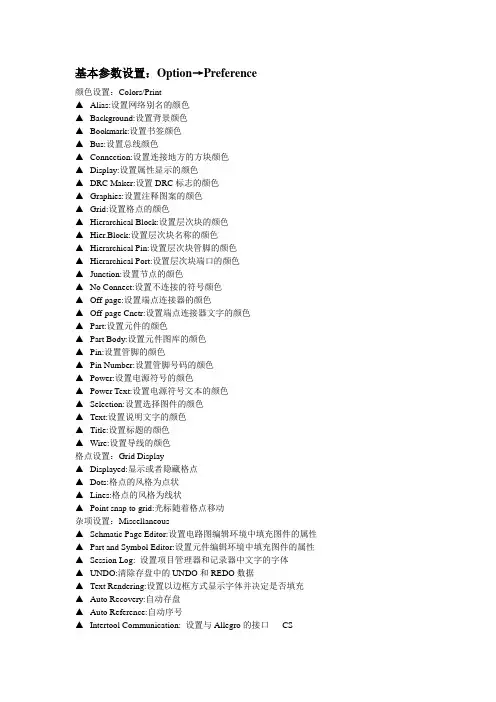
基本参数设置:Option→Preference颜色设置:Colors/Print▲Alias:设置网络别名的颜色▲Background:设置背景颜色▲Bookmark:设置书签颜色▲Bus:设置总线颜色▲Connection:设置连接地方的方块颜色▲Display:设置属性显示的颜色▲DRC Maker:设置DRC标志的颜色▲Graphies:设置注释图案的颜色▲Grid:设置格点的颜色▲Hierarchical Block:设置层次块的颜色▲Hier.Block:设置层次块名称的颜色▲Hierarchical Pin:设置层次块管脚的颜色▲Hierarchical Port:设置层次块端口的颜色▲Junction:设置节点的颜色▲No Connect:设置不连接的符号颜色▲Off-page:设置端点连接器的颜色▲Off-page Cnctr:设置端点连接器文字的颜色▲Part:设置元件的颜色▲Part Body:设置元件图库的颜色▲Pin:设置管脚的颜色▲Pin Number:设置管脚号码的颜色▲Power:设置电源符号的颜色▲Power Text:设置电源符号文本的颜色▲Selection:设置选择图件的颜色▲Text:设置说明文字的颜色▲Title:设置标题的颜色▲Wire:设置导线的颜色格点设置:Grid Display▲Displayed:显示或者隐藏格点▲Dots:格点的风格为点状▲Lines:格点的风格为线状▲Point snap to grid:光标随着格点移动杂项设置:Miscellaneous▲Schmatic Page Editor:设置电路图编辑环境中填充图件的属性▲Part and Symbol Editor:设置元件编辑环境中填充图件的属性▲Session Log: 设置项目管理器和记录器中文字的字体▲UNDO:清除存盘中的UNDO和REDO数据▲Text Rendering:设置以边框方式显示字体并决定是否填充▲Auto Recovery:自动存盘▲Auto Reference:自动序号▲Intertool Communication: 设置与Allegro的接口CS▲Wire Dray:在设置改变时允许元件的移动设计模板的设置:Option→Design TemplateFonts:设置设计模板中的字体Title Block:设置标题块的内容和格式Page Size:设置单位、页面尺寸的大小和管脚间距▲Units:设置英制和公制▲A~E:设置页面尺寸的宽度和高度▲Custom:设置自定义页面尺寸的大小▲Pin-to-Pin Spacing:设置管脚间距Grid Reference:设置栅格点▲Count:分别设置水平边框和垂直边框的参考格的格数▲Alphabetic:分别设置水平边框和垂直边框的格位以字母编号▲Numeric: 分别设置水平边框和垂直边框的格位以数字编号▲Descending:分别设置水平边框和垂直边框的格位编号从右到左▲Width:分别设置水平边框和垂直边框的格位高度▲Displayed:分别设置显示边框和边框参考格位以及标题栏▲Printe:分别设置打印边框和打印边框参考格位以及标题栏▲ANSI grid references:设置显示ANSI标准格点Hierarchy:设置层次式电路图的属性▲Primitive:设置层次电路图和元件为基本组件▲Nonprimitive:设置层次电路图和元件为非基本组件SDT Compatibility:设置SDT格式电路图的兼容性。
Cadence-Menu--cadence软件菜单中英文对照图
TP-
移动
编辑页和符号
下一层菜单见下表
编辑层
同上
返回
页脚内容1
改变组件
设置启动的工具
祭看搜索栈
物理输出
进行封装并输出
物理输入
从Allegro导入
IFF输入
导入IFF文件
打印设置
打印预览
打印输出
可输出原理图
退出
注:若菜单中的说明项为空,则表示不不需要说明或说明项与中文菜单相似。以下相同
撤销
UiadoCtrlf-Z
pf=rinCrrlJ-V
Co&y All
页脚内容2
Edit P^ge/Symbof
Edit Hierarchy
Change 5uite..・
Viev^
保存
卜
另存为
~F~
保存所有
保存层
Export Physical.,. lmpcrt Physical...
吁…
转换
Plot Setijp...
Plot Preview...
Plot.-t,Ctr
电ቤተ መጻሕፍቲ ባይዱt
第二部分
菜单栏
文件、编辑、察看、器件、连线、文本、模块、组、显示、PSpice、工具、窗口、帮助
1文件菜单
原菜单
中文菜单
说明
Nevj匚tr
Qpan....匚"
Close
Save.Ctr
Save All...
Save Hierarchy
+N
+0
新建
+S
打开
关闭
Revert
Reto yer...
Rernove..»
altium窗口菜单中英文对照表
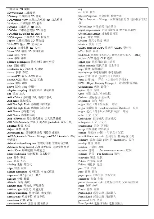
- ..Altium_Designer(protel_DXP)英文菜单汉化对应表表2021-01-08 17:065964人阅读评论(0)收藏举报分类:硬件〔100〕%s - No SI model for part%s - 没有部件的SI模型%s Degrees%s 度%s mm%s 毫米%s object selected in %s document在%s个文档有%s个对象被选中%s Objects Displayed (%s Selected)%s 对象显示(%s 被选择)%s objects selected%s 对象被选择(custom)(自定义)(pixels)(像素)+12 Power Port+12 电源端口+5 Power Port+5 电源端口-5 Power Port-5 电源端口0 Hidden ment strings0 隐藏注释行0.01uF Capacitor0.01uF 电容0.1uF Capacitor0.1uF 电容1 Locked ponents1 锁定元件1 By Ascending X Then Ascending Y根据X递增量决定Y递增量1.0uF Capacitor1.0uF 电容100K Hertz Pulse100KHz 脉冲100K Hertz Sine Wave100KHz 正弦波100K Resistor100K 电阻10K Hertz Pulse10KHz 脉冲10K Hertz Sine Wave10KHz 正弦波10K Resistor10K 电阻10uF Capacitor10uF 电容1K Hertz Pulse1KHz 脉冲1K Hertz Sine Wave1KHz 正弦波1K Resistor1K 电阻1M Hertz Pulse1MHz 脉冲1M Hertz Sine Wave1MHz 正弦波2 Pads and vias with a hole size between 15and 302 焊盘和过孔的孔大小在15-30之间2.2uF Capacitor2.2uF 电容4 All testpoints4 全部测试点4 Port Serial Interface4 端口串行接口4.7K Resistor4.7K 电阻47K Resistor47K 电阻5 ponent track and arc silkscreenprimitives5 元件丝印层的根本线和弧线A KeywordA关键字Abort Simulation终止仿真About Design Explorer关于设计浏览器Absolute绝对Absolute Layer绝对层Absolute Origin绝对原点AC Small Signal Analysis Setup交流小信号分析配置Accept Changes (Create ECO)成认改变(建立ECO)Access Code验证码Accuracy精度Activates open documents激活显示文本Active Low Input激活低电平输入Active Low Output激活低电平输出Active project当前激活工程Active sheet当前激活图纸Active Signals激活的信号Add All添加全部- ..Add All Waveforms添加全部波形Add as Rule作为规那么添加Add Assembly Outputs增加装配输出Add Class添加分类Add ponent Part添加元件部件Add Document增加文本Add Document to Focused Project添加文档到当前工程Add Documentation Outputs增加文本输出Add Existing Project添加已存在的工程Add Fabrication Outputs增加生产输出Add first condition添加首要条件Add From To添加From ToAdd Internal Plane增加电层Add Layer添加层Add Library添加库Add License添加许可证Add Net添加网络Add Net Class添加网络分类Add Netlist Outputs增加网表输出Add New Cursor增加标Add New Model添加新模式Add New Project添加新工程Add One添加一个Add or Remove Libraries添加或移出库文件Add Other Outputs添加其他输出Add Plane添加电层Add Plot增加图表Add Project To Version Control将工程添加到版本控制Add Remove ponent Libraries添加移出元件库Add Remove Libraries添加/移出库文件Add Reports增加报告Add Selected添加选择的Add Selected Primitives to ponent添加所选根本元素到元件Add Sheet Entry添加图纸入口Add Signal Layer增加信号层Add Suffix加后缀Add Template to Clipboard添加模板到剪贴板Add To Current Sheet添加到当前图纸Add to Custom Colors添加到自定义颜色Add To Design添加到设计Add To Entire Project添加到整个工程Add to new Y axis增加到新Y轴Add to Project添加到工程Add To Sheet添加到图纸Add To Version Control添加到版本控制Add top level signals to waveform给波形增加顶层信号Add Variant添加变量Add Watch增加监视Add Wave增加波形Add Wave To Plot给图表增加波形Add Waveform增加波形Add waveforms to the new plot给新图表增加波形Add Y Axis增加Y 轴Add/Edit Model增加/编辑模型Add/Remove Libraries装载/移出库文件Add/Remove Library装载/移出库AddAlias添加别名Advanced (Query)高级(查询)Advanced Mode高级模式Affected Document所影响的文本- ..Affected Object所影响的对象Aggregate合计Align Bottom底部对齐Align ponents对齐元件Align ponents by Bottom Edges根据元件下缘对齐Align ponents by Horizontal Centers元件居中对齐Align ponents by Left Edges元件左边对齐Align ponents by Right Edges元件右边对齐Align ponents by Top Edges元件对齐顶部边缘Align ponents by Vertical Centers根据垂直中心对其元件Align Left左对齐Align Right右对齐Align Top顶部对齐Aligned - Bottom对齐- 底部Aligned - Center对齐- 中心Aligned - Inside Left对齐- 部左边Aligned - Inside Right对齐- 部右边Aligned - Left对齐- 左边Aligned - Right对齐- 右边Aligned - Top对齐- 顶部all全部All ponents全部元件All Draft全部草图All Final全部最终All Hidden全部隐藏All Locked全部锁定All Nets全部网络All Off全部关闭All On全部翻开All On Current Document全部当前文档All on Layer全部翻开层All open schematic documents所有翻开原理图文档All Orientations所有方向All schematic documents in the currentproject当前工程中所有原理图文档All Text Docs全部文本文件Allow Dock允许停放Allow multiple testpoints on same net允许同一网络多个测试点Allow Ports to Name Nets允许端口到网络名Allow Sheet Entries to Name Nets允许图纸入口到网络名Allow Short Circuit允许电路短路Allow Synchronization With Database允许和数据库同步Allow Synchronization With Library允许和库同步Allow testpoint under ponent元件下允许测试点Allow Vias under SMD PadsSMD焊盘下允许过孔Allowed Orientations允许方向Allowed Side and Order允许边和定制Alpha字母Alpha Numeric字母数字Alpha Numeric Suffix字母数字下标Alphabetically字母顺序Alternate 1另一选择1Alternative其他选择Always load error file总是加载错误文件Amplitude振幅Analog模拟Analog +12V (+12V)模拟+12V (+12V)Analog +5V (+5V)模拟+5V (+5V)Analog Ground (AGND)模拟地(AGND)Analog Routing 1模拟布线层1Analog Routing 2模拟布线层2- ..Analog Routing 3模拟布线层3Analog Signal In模拟信号输入Analyse分析Analyses Setup分析配置Analyses/Options分析/选项Analysis分析Analysis Errors分析错误Analyze Design分析设计Analyze Document分析文档And Gate与门And to wrap long lines增加到可交换长行Angular角形Angular Dimension角度Angular Step角幅Animation speed动画速度Annotate标注Annotation注释Anode正极ANSIANSIAny任何Aperture File (using Wizard formats)光圈文件(利用向导格式) Aperture Library光圈库Aperture List光圈列表Aperture Matching TolerancesD码表匹配公差Append Sheet Numbers to Local Nets附加图纸编号到本地网络Applicable Binary Rules适用的二元规那么Applicable Rules适用的规那么Applicable Unary Rules适用的一元规那么Apply Filter应用过滤器Apply to Active Chart Only仅适用于激活图表Apply to Entire Document适用于整个文本Arc弧线Arc (Any Angle)弧形(任何角度)Arc (Center)弧形(定中心)Arc (Edge)弧形(边限)Arc Line Width弧线宽度Arc Radius圆弧半径Architecture构造Archive project document存档工程文件Arcs弧形Arithmetic算法Around Point附近的点Arrange All Windows Horizontally水平排列所有窗口Arrange All Windows Vertically垂直排列所有窗口Arrange ponents Inside Area在区域排列元件Arrange ponents Within Room在布局空间排列元件Arrange Outside Board在底边界外排列Arrange Within Rectangle在矩形里排列Arrange Within Room在布局空间里排列Arrow Length箭头长度Arrow Line Width箭头线宽度Arrow Position箭头位置Arrow Size箭头大小Arrow Style Power Port发射型电源端口Arrow Width箭头宽度Articles and Tutorials文章和教程Assembly %s装配%sAssembly Drawings装配制图Assembly Outputs装配输出At Margin在页边距- ..At Window在窗口Attributes on Layer层上属性Auto Create posite自动创立合成Auto indent mode自动缩进模式Auto Pan Fixed Jump自动平移固定围Auto Pan Off自动平移关闭Auto Pan Options自动平移选项Auto Pan ReCenter自动平移至中心Auto Placement自动布局Auto Placer自动放置Auto Route自动布线Auto save every自动保存间隔Auto Zoom自动缩放Auto-Increment During Placement在布局时自动增加Auto-Junction自动加节点Auto-Position Sheet自动定位图纸Automatic (Based on project contents)自动〔基于工程容〕Automatically crossprobe first error自动穿插检索第一个错误Automatically Remove Loops自动去除回路Autopan Options自动位移选项Autoposition自动定位Autosave desktop自动保存桌面设置Available Libraries当前库Available Routing Strategies可用的布线策略Available Signals可用的信号Average Track Length (mil)平均铜线长度〔mil〕Avg平均Avoid Obstacle避开障碍物Back Annotate反向标注Background背景Backspace unindents回车取消缩进Backup Files备份文件Backup Options备份选项Ball Grid Arrays (BGA)BGABallistic可变速度移动Bank1组列1Bank2组列2Bar Style Power Port条型电源端口Bar to use as Main Menu栏作为主菜单使用Bar Type栏类型Bars栏Base Value低电平Baseline基线Baseline Dimension基线尺度Basic DC根本直流Batch批处理Batch Mode批命令模式Begin Group开场分组Below is a list of all the processesprovided by this server以以下表是此效劳提供的所有处理模块Beta DegBeta降级Bezier曲线BGA OptionsBGA 选项Bidirectional Signal Flow双向信号流向Bill of Materials材料清单Bill of Materials (By PartType) For Project[%]工程[%s]物料清单(元件类型)Bill of Materials For PCB%sPCB %s材料清单Bill of Materials For Project %s工程材料清单%sBitmap File位图文件Blank Project (Embedded)空白工程(嵌入式)- ..Blank Project (FPGA)空白工程(FPGA)Blank Project (Library Package)空白工程(库包) Blank Project (PCB)空白工程(PCB)Block Indent块缩进Block Name块名称Block Name : %s块名称: %sBoard板Board Area Color板区域颜色Board Dimensions板尺寸Board in 3D3D 板视图Board Information板信息Board La&yers & Colors板层和颜色Board La&yers && Colors板层和颜色Board Layers Colors板层颜色Board Layers & Colors板层和颜色Board Layers and Colors板层和颜色Board Line Color板层线颜色Board Options板选项Board Shape板形Board Specifications板技术参数Bold Waveforms实线波形BOOLEAN布尔数学体系Border (Auto-Detect)边界(自动探测)Border Color边框颜色Border On边框显示Border Width边框宽度Bottom底层Bottom Dielectric底部绝缘层Bottom Layer底层Bottom Layer Annular Ring Size底层圆环尺寸Bottom Overlay底层丝印层Bottom Paste底层焊锡层Bottom Solder底层阻焊层Bottom Solder Mask底层阻焊层BottomLayer底层BottomOverlay底层丝印层Brackets支架Break All ponent Unions从单元中别离出所有元件Break ponent from Union从单元中别离出元件Break Track断开轨迹Breakpoints断点Brightness亮度Bring To Front Of带到某对象前面Browse浏览Browse ponent Libraries浏览元件库Browse ponents浏览元件Browse Libraries浏览库Browse Library浏览库文件Bubble Help Advisor (Shift+F1)浮动帮助参谋(Shift+F1) Build posite构造合成Build Later后来再建Build PCB Project构造PCB 工程Build Project构造工程Build Query构造智能语句Build Sooner立即创立Build-Up绝缘层对Building Query from Board从板构造查询Bus总线Bus Entry总线入口Bus indices out of range总线超出围- ..Bus range syntax errors总线围语法错误Bus Width总线线宽By class通过类By document type通过文本类型C MenuC 菜单C StandardC 标准Calc. Copper Area计算.铜面积Calculated Impedance =计算阻抗=Calculated Trace Width =计算线宽=CAM DocumentCAM 文档CAM EditorCAM 编辑器Cannot Locate Document %s无法找到%s文档信息Capacitance电容Capacitor电容Capacitors电容Categories类别Cathode负极Center Dimension中心点尺度Center Horizontal水平居中Center of Object对象中心Center Vertical垂直居中Change Language更换语言Change Order改变顺序Change System Font改变系统字体Change Technology改变封装技术Channel Offset通道偏移Characteristic Impedance Driven Width特性阻抗驱动线宽Chart制图Chart name is blank图表名称为空Chart Options图表选项Check All ponents检查所有元件Check In签入Check Mode校验模式Check Out签出Check Syntax校验语法Choose a snap grid size选择捕获网格尺寸Choose Color选择颜色Choose cursor to delete选择要光标删除Choose cursor to jump to选择要跳转到的光标Choose Default Backup Folder选择缺省的备份文件夹Choose Default Document Folder选择缺省文档文件夹Choose Design Rule Type选择设计规那么类型Choose Document选择文档Choose Document Scope选择文档围Choose Document to Open选择要翻开的文档Choose Document to Place选择文档放置Choose Documents选择文档Choose Documents to Add to Project %s选择文档加到工程%sChoose Documents To pare选择比拟文档Choose documents to pare - one from theleft list and one from the right list选择比拟文档- 一个从左面列表另一个从右面列表选择Choose Project选择工程Choose Project Group to Open选择要翻开的工程组Choose Project to Open选择要翻开的工程Choose second corner选择第二角Choose the document to pare against thedesign hierarchy of %s选择与设计层次%s进展比拟的文本Choose the document to pare against thedesign hierarchy of Documents.PRJPCB选择与工程文本的层次设计进展比拟的文本Choose Top Level选择顶层- ..Choose WAS-IS File for Back-Annotation fromPCB从PCB选择WAS-IS文件作为反向注释Circle Style Power Port循环型电源端口Circuit电路Circuit Simulation电路仿真CKTCKTClamping箝位Class I分类IClass II分类IIClass Type类型Classes分类Classic Color Set典型颜色设置Clean All Nets去除全部网络Clean Single Nets去除单一网络Clear All Nets去除全部网络Clear All Test points去除全部检测点Clear All Testpoints去除全部测试点Clear Browser Marks去除浏览器标记Clear Class去除类别Clear Current Filter去除当前过滤器Clear Current Filter (Shift+C)去除当前过滤器(Shift+C)Clear Existing去除已存在Clear Filter去除过滤器Clear History去除历史Clear Memory去除存储器Clear non-numerical values去除非数字的值Clear Selected去除已选Clear Status去除状态Clear workspace pile messages onpile编译时去除工作空间编译信息Clearance间距Click Clears Selection单击去除选择Click on the finish button to plete thetask在完毕按钮上点击完成任务Client客户端Client License Usage客户端许可证用法Client Setup客户端设置Clip to Area显示框文本Clipboard Reference剪贴板属性clock时钟Close 'pile Errors'关闭‘编译错误’面板Close 'piled Object Debugger'关闭‘编译对象调试器’面板Close 'Differences'关闭‘差异’面板Close 'Files'关闭‘文件’面板Close 'Help Advisor'关闭‘帮助参谋’面板Close 'Inspector'关闭'检视器'Close 'Libraries'关闭'库'Close 'List'关闭'列表'Close 'Messages'关闭‘消息’面板Close 'navigator'关闭‘浏览器’面板Close 'Projects'关闭‘工程’面板Close All Documents关闭全部文件Close posite关闭合成Close Documents关闭文档Close Focused Project关闭当前工程Close Project关闭工程Close Project Documents关闭工程文档Collapse Row折叠行Collect Data For数据收集类型Collector集电极Color Options颜色选项Color Set颜色设置- ..Colors && Gray Scales色彩/灰度级Colours颜色Column Best Fit适应列宽mand Reference命令参考mand Status命令状态栏ment type注释类型p Drag拖动比拟parator比拟器parison Type Description比拟类型描述pile Active Document编译当前文档pile Active Project编译当前工程pile All编译全部pile All Open Projects编译全部已翻开的工程pile All Projects编译所有工程pile Current Project编译当前工程pile Document编译文档pile Errors编译错误pile FPGA Project编译FPGA 工程pile Later后来再编译pile Library编译库pile only if modified仅编译修改之后pile PCB Project编译PCB 工程pile Project编译工程pile Sooner立即编译piled编译piled Object Debugger编译对象调试器piler Options编译选项piling %s正在编译%spiling Flattened Project编译平行工程plex Data复杂数据ponent元件ponent %s元件%sponent Actions元件操作ponent Class Generator元件分类发生器ponent Classes元件分类ponent ment元件注释ponent Connections元件连接ponent Cross Reference元件互相参照ponent Cross Reference Report ForProject %s工程元件穿插参考报告%s ponent Designator%s元件标识符%sponent Grid元件网格ponent Links元件ponent Name部件名ponent Names元件名称ponent Naming元件命名ponent Nets元件网络ponent Parameter元件参数ponent Pin Designator元件引脚标识符ponent Pin Editor元件引脚编辑器ponent Pins元件引脚ponent Placement元件布局ponent Primitives元件根本元素ponent Properties元件属性ponent Report元件报告ponent Rule Check元件规那么检查ponent scope for filtering andselection过滤及选择元件的围ponent Side元件层ponent Type元件类型ponent Types元件类型ponent Wizard元件向导- ..ponent Wizard - Pin Grid Arrays (PGA)元件向导- PGAponents元件ponents Cut Wires元件切线posite Drill Guide合成钻孔向导posite Layers合并层posite Properties合成特性Condition Type / Operator类型/操作状态Condition Value条件值Conductor Width导体宽度Conductors导体Configure Drill Pairs配置钻孔层对Configure Licenses配置软件许可证Configure PLD piler配置PLD编译Configure Project Options for ActiveProject为当前工程配置工程选项Confirm Delete Parameter确认删除参数Confirm Global Edit确定全局编辑Confirm Remove %s确认删除%sConfirm remove the layer %s确认是删除层%sConfirm Selection Memory Clear选择存储器去除时确认Connect Layer连接层Connect Style连接样式Connect To连接到Connect to Net连接到网络Connect Wire Check接线检查Connect Wire Extractor接线数据Connected Copper连接铜线Connected Tracks连接铜线Connection Color连接颜色Connection Matrix连接矩阵Connector连接器Connector Type连接器类型Constant Level常数等级Constraints约束限制Contract All全部压缩Convert Part To Sheet Symbol转换元件为图纸符号Convert Selected Free Pads to Vias将所选自由焊盘转换为过孔Convert Selected Vias to Free Pads将所选过孔转换为自由焊盘Convert Special Strings转换特殊字符串Convert to DXP Plane Mode转换为DXP电层模式Coordinate坐标Coordinate Positions坐标位置Copper thickness铜厚度Copy (Ctrl+C)复制(Ctrl+C)Copy ponent复制元件Copy Footprint From/To复制封装从/到Copy on Field复制域Copy preexisting edif models whenavailable当可访问到时拷贝已经存在的EDIF模型Copy Room Formats复制布局空间格式Copy to Layers复制到层Copyright ?Altium Limited 2002 Altium 所有2002Core (%s)核心(%s)Corner角Corner 1角1Corner 2角2Corrections校正Coupling耦合Create a new Board Level Design Project创立新的板级设计工程Create a new FPGA Design Project创立新的FPGA设计工程Create a new Integrated Library Package创立新的集成库包Create backup files创立备份文件- ..Create piled SimCode output file创立编译SimCode输出文件Create ponent创立元件Create Engineering Change Order创立工程改变顺序(ECO)Create Expression创立表达式Create FFT Chart新建FFT图表Create Library创立库Create List From PCB从PCB建表Create Netlist From Connected Copper从连接的铜板创立网表Create New Chart新建图表Create New Database新建数据库Create Non-Orthoganal Room from selectedponents根据所选元件创立非正交布局空间Create Non-Orthogonal Room from ponents根据元件创立非正交布局空间Create Orthogonal Room from ponents根据元件创立正交布局空间Create Orthogonal Room from selectedponents根据所选元件创立正交布局空间Create Pairs From Layer Stack从层堆栈中创立层对Create Pairs From Used Vias从所用过孔中创立层对Create Projects from Path从指定路径创立工程Create Rectangle Room from selectedponents根据所选元件创立矩形布局空间Create Rectangular Room from ponents根据元件创立矩形布局空间Create Report建立报告Create Report File创立报告文件Create Rule创立规那么Create Sheet From Symbol从符号创立图纸Create Symbol From Sheet从图纸创立符号Create Union from ponents从元件创立单元Create Union from Selected ponents根据所选元件创立单元Create VHDL File From Symbol从符号创立VHDL 文件Create VHDL from FPGA-Part从FPGA 零件创立VHDLCreate VHDL Testbench创立VHDL 测试平台Create Violations创立违规信息Cross Probe插入探针Cross Probe to Documents文档中插入探针Cross Probe to Schematic穿插检索到原理图Crossing Window穿插窗口Crossprobe schematic穿插检索原理图Crosstalk串扰Crosstalk Analysis串扰分析Crosstalk Waveforms串扰分析CTRL+Double Click Opens SheetCTRL+双击翻开图纸Current ponent当前元件Current Document当前文档Current Font当前字体Current Layer当前层Current Origin当前原点Current Page当前页Cursor A光标ACursor B光标BCursor beyond EOFEOF的光标Cursor beyond EOLEOL的光标Cursor Grid Options指针网格选项Cursor through tabs通过Tab移动光标Cursor Type光标类型Curve Width曲线宽度Custom Aperture Library File (*.LIB)自定义光圈库文件(*.LIB)Custom Height自定义高Custom Size自定义大小Custom Step定制调试Custom Style自定义风格Custom Width自定义宽- ..Customize Resources自定义资源Customizing DefaultEditor Editor用户缺省自定义编辑器Customizing PCB Editor自定义PCB 编辑器Customizing PCBLib Editor自定义PCBLib编辑器Customizing Sch Editor自定义原理图编辑器Customizing SchLib Editor定制原理图库编辑器Customizing VHDL Editor自定义VHDL编辑器Cut (Ctrl+X)剪切(Ctrl+X)Cutout挖除局部Darken调暗Data Process接线数据处理Database Connection数据库连接Database key field数据库关键字段Database Link File数据库文件Database Link Options数据库选项Database Linking数据库Database Linking Menu数据库菜单Database Links数据库DatabaseLink数据库Datasheet数据表Datum数据Datum Dimension数据尺度DC AnalysisDC分析DC Sweep Analysis Setup直流扫描分析配置Debugging Options调试选项Decision判定Declare ponent At Cursor在指针指向元件显示说明Decrease减少Decrease Horizontal Spacing of ponents减小元件水平间距Decrease Priority降低优先级Decrease Vertical Spacing of ponents减小元件的垂直间距default默认Default Background默认背景Default Bars缺省面板Default Color Set默认颜色设置Default Designator缺省名称Default File Name缺省文件名Default Locations默认位置Default Power Object Names默认电源对象名称Default Primitives默认根本元素Default Prints默认打印Default Shortcuts默认快捷方式Default Stimulus默认鼓励Default Template Name缺省模板名Default time units默认时间单位Default Value默认值Default Vendor Family默认厂家芯片系列DefaultEditor默认编辑DefaultRowHeight默认行高Define from selected objects从所选对象定义Define the layout of the PGA footprint byselecting the proper values选择适当的值定义PGA封装引脚布局degrees度数Delete All全部删除Delete All Cursors删除全部光标Delete All Waveforms删除全部波形Delete Chart删除图表Delete Class删除分类Delete Current Cursor删除当前光标Delete Cursor删除光标- ..Delete generated files before pile编译之前删除生成的文件Delete Net删除网络Delete Net Class删除网络分类Delete Plot删除坐标图Delete Watch删除监视Delete Waveform删除波形Delta Step增量调试Demote降级Density Map密度图Deselect All取消全部选择DeSelect All On Current Document取消选择当前的全部文档Design设计Design Documents设计文本Design Explorer DXP DXP 设计浏览器Design Explorer DXP - %s设计浏览器DXP - %sDesign Explorer Error设计浏览器错误Design Explorer Information设计浏览器信息Design Explorer Preferences设计浏览器属性Design Explorer Project Manager设计浏览器工程管理器Design Explorer Version 7.1.70设计浏览器版本7.1.70 Design Explorer Version 7.2.92设计浏览器版本7.2.92 Design Explorer Warning设计浏览器告警Design Rule Check设计规那么检查Design Rule Checker设计规那么检查Design Rules设计规那么Designator标识符Designator Display标识符显示Designator Format标识符格式Designator Index Control标识符指针控制Designators标识符Destination Library目标库Device Family器件系列Dielectric constant绝缘材料常数Dielectric Properties绝缘体属性Differences差异Different不同Digital Ground (GND)数字地层(GND)Digital Objects数字对象Digital Power (VCC)数字电源层(VCC)Digital Routing 1数字布线层1Digital Routing 2数字布线层2Digital Routing 3数字布线层3Digital Routing 4数字布线层4Digital Routing 5数字布线层5Digital Routing 6数字布线层6Digital Signal In数字信号输入Digital supply VCC数字电源VCCDigital Supply VDD数字电源VDDDimension标注线Dimensions标注线Diode二极管Diodes二极管Direction From Pad出焊盘方向Directive Options提示选项Directives指令Disable不激活Disable All全部禁用Disable All Watches禁用全部监视Disable dragging取消拖动Disable Update All取消修改全部- ..Disable Update Selected取消修改选择的Disable Watch禁用监视Display Cross Sheet Connectors显示图纸间连接符Display FFT Charts显示FFT图表Display Full Hierarchy显示全部层次Display Graphical Lines显示图形线条Display Logical Designators显示逻辑标识符Display Mode显示模式Display Name显示名称Display Net Labels显示网络标志Display No Hierarchy显示没有层次图Display Options显示选项Display Physical Designators显示物理标识符Display Pins显示引脚Display Ports显示端口Display Printer Fonts显示打印字体Display Report显示报告Display shadows around menus, toolbars andpanels显示菜单, 工具栏, 面板的阴影Display Sheet显示图纸Display Sheet Entries显示图纸入口Display Sheet Symbols显示图纸符号Display Symbols显示符号Display System Information显示系统信息Distance factor距离因素Distribute Horizontally水平居中分布Distribute Vertically垂直居中分布Division Size分割尺度Do not group不分组Do you wish to delete the Parameter你希望删除这个参数Documen文本Document Editors文档编辑器Document Name文档名称Document Options文档选项Document Order文档顺序Document Parameters文本参数Document Path文档路径Document scope for filtering and selection过滤选择文档围Documentation %s文本%sDocumentation Output文本输出Documents for %s%s 文档Documents for Free Documents文档为自由文档Does nothing无任何操作Don't Annotate ponent不注释元件Don't care不关注dot点Dot Grid网格点Dotted点Double click line双击行Double Click Runs Inspector鼠标双击那么运行检视器Double Sided双面Draft Thresholds草图起点Drag拖动Drag a column header here to group by thatcolumn拖动一列标头到这列用于分组Drag Orthogonal直角拖动Drag Selection拖动选择容Drag Track End拖动轨迹末端Draw Solid画实线Draw to Custom Aperture自定义光圈绘图Drawing制图Drawing Tools制图工具- ..DRC Error MarkersDRC 错误标记DRC Report OptionsDRC报告选项DRC ViolationsDRC违规数Drill钻孔机Drill Drawing钻孔图Drill Drawing Plots钻孔绘制图Drill Drawing Symbols钻孔绘制符号Drill Drawings钻孔图Drill Guide钻孔向导Drill Guide Plots钻孔导向图Drill Pair Properties钻孔层对属性Drill Pairs钻孔配对层Drill-Pair Manager钻孔层对管理器Drill-Pair Properties钻孔对属性DrillDrawing钻孔图DrillGuide钻孔向导Dual in-line Package (DIP)DIPDuplicate Selected复制被选DXP Help AdvisorDXP 帮助指导DXP Knowledge BaseDXP 知识库DXP Learning GuidesDXP 学习指南DXP Online helpDXP 在线帮助Dynamic动态Dynamic transparency动态透明效果Earth接地Earth Power Port接地电源端口ECO GenerationECO 启动EDA ServersEDA 效劳Edge Connectors边缘连接器EDIF MacroEDIF宏EDIF MenuEDIF 菜单EDIF StandardEDIF 标准Edit Buffer编辑缓冲Edit mand编辑命令Edit ment编辑注释Edit Full Pad Layer Definition编辑完整的焊盘层Edit Keyword Properties编辑关键字属性Edit Language Syntax编辑语言语法Edit Layer编辑层Edit Library编辑库Edit Net编辑网络Edit Net Class编辑网络分类Edit Nets编辑网络Edit Number编辑编号Edit Pins编辑引脚Edit Polygonal Room Vertices编辑多边形空间的顶点Edit Rule Priorities编辑规那么优先级Edit Rule Values编辑规那么数值Edit Selected编辑被选Edit Simulation Signals编辑仿真信号Edit String编辑字符串Edit Style编辑风格Edit Values编辑值Edit Variant编辑变量Edit Wave编辑波形Editing Options编辑选项Editor Preferences参数选择编辑器EditScript编辑脚本Eight Layer (5 x Signal, 3 x Plane)八层〔5信号层,3电层〕Elaborate and generate on pile编译时详细阐述和产生- ..Electrical Grid电子网格Electrical Type电气类型Ellipse椭圆形Elliptical Arc椭圆的弧线Embedded嵌入Embedded apertures (RS274X)嵌光圈表[RS274X]Embedded Project嵌入式工程Embedded Projects嵌入式工程Emitter发射极Enable All全部启用Enable All Watches启用全部监视Enable Font Substitution允许字型替换Enable In-Place Editing启用位置编辑Enable Update All使能修改全部Enable Update Selected使能修改选择的Enable Version Control允许版本控制Enable Watch启用监视Enabled激活End Angle完毕角度End Layer完毕层Enforce layer pairs settings执行层对设置Engineering Change Order工程改变单Entity/Configuration实体/配置Equalize Net Lengths补偿网络长度Error Marker错误标记Error Reporting错误报告Errors Detected监测到错误Errors or warnings found发现错误或告警Esc取消Example Layer Stacks层堆栈举例Examples例Excel Template FilenameExcel 模板文件名Exclude IEEE Directory不包括IEEE目录Exclude System Parameters拒绝系统参数Execute Changes执行改变Expand Row扩展行Expansion扩展Expansion value from rules从规那么扩展值Expiry Date有效期限Explode拆解Explode ponent to Free Primitives将元件拆解为自由的根本元素Explode posite拆解合成Explode Coordinate to Free Primitives将坐标拆解为自由的根本元素Explode Dimension to Free Primitives将尺度标注拆解为自由的根本元素Explode Polygon to Free Primitives将多边形敷铜拆解为自由的根本元素Explore浏览Explore Differences探测差异ExplorerFramePanel管理器框架面板Exponential/Logarithmic指数/对数Export Grid Contents导出容Export Netlist From PCB从PCB 导出网表Export Selected Waveforms导出选择的波形Export to PCB导出到PCBExport Using Template导出使用模板Expression表达式Extension Width延伸宽度Fabrication %s生产%sFabrication Outputs生产输出Falling Edge Flight Time下降沿延迟时间Falling Edge Overshoot下降沿过冲- ..Falling Edge Slope下降沿斜率Falling Edge Undershoot下降沿下冲False错误Fanout扇出Fanout DirectionFanout 方向Fanout OptionsFanout 选项Fanout StyleFanout 风格faster快Fatal Error严重错误File Mask文件过滤Files Found on All Search Paths在全部路径上查找到的文件Fill Color填充颜色Fills填充Film Box胶片盒Film Size胶片尺寸Film Wizard胶片向导Filter过滤Filter browsed objects过滤浏览对象Filter For过滤Filtered Objects过滤对象Final最终Final Properties最终属性Find and Replace Text查找并替换文本Find and Set Testpoints选择和设置测试点Find ponent查找部件Find Coupled Nets发现耦合网络Find Selections查找选择容Find Similar Objects找出相似对象Find text at cursor光标位置查找文本First ponent第一个元件First Layer首层First Page首页First Transition首次转换Fit All Objects适合全部对象Fit Board适合底板Fit Document适合大小文档Fit Document (Ctrl+PgDn)适合大小文档(Ctrl+PgDn)Fit Filtered Objects适合过滤对象Fit Selected适合选择Fit Selected Objects适合选中对象Fit Sheet适合图纸Fit Specified Area适合指定区域Fit Waveforms适合波形Fixed Size Jump固定步长跳转Flat (Only ports global)平面〔只对全局端口〕Flip Selection翻转被选FLOAT浮点Focus Wave主波形Font Substitutions字型置换Footprint封装Footprint Model封装模型Footprint not found没有发现封装Footprints封装For a parallel gap of平行线间距Force Columns Into View所有列显示Force plete tenting on bottom在底部强制完全伸展Force plete tenting on top在顶部强制完全伸展Foreground前景Formal Type格式类型Format and Radix格式和基数- ..Format Axis格式化轴Format Wave格式化波形Format Y Axis格式化Y 轴Formats格式Formatting格式化Found in发现于Four Layer (2 x Signal, 2 x Plane)四层〔2信号层,2电层〕FPGA OptionsFPGA 选项FPGA PreferencesFPGA 参数选择FPGA ProjectFPGA工程FPGA ProjectsFPGA工程Free Documents自由文档Free Objects自由对象From To Display Settings飞线显示设置From Tos飞线From-To Editor飞线编辑器Full Circle圆环Full line ment全行注释Full Query完全查询Full Results全部结果Full Stack完全层叠Function Definitions函数定义Gap间隙Gear 2齿轮2Gear 3齿轮3Gear 4齿轮4Gear 5齿轮5Gear 6齿轮6Gear's Method 1st Order齿轮方法第1命令Gear's Method 2nd Order齿轮方法第2命令Gear's Method 3rd Order齿轮方法第3命令Generate Change Orders产生改变命令Generate DRC Rules产生DRC规那么Generate implicit modules for LPM, XBLOX orLogicB为LPM, XBLOX orLogicB产生隐含模块Generate Print Preview of Active Document生成激活文档的打印预览Generate Report生成报告Generate XSPICE Netlist生成XSPICE 连线表Generates pick and place files生成拾取和摆放文件Gerber FilesGerber文件Gerber SetupGerber设置Get Latest Version得到最后的版本Global (Netlabels and ports global)全局〔网络标号和全局端口〕GND Power Port接地电源端口Goto Line Number转到连线编号Graph图表Graphic图形Graphical图形Graphical Editing图形编辑Greater Equal大于等于Grid栅格Grid 1网格1Grid 2网格2Grid Color网格颜色Grid Range网格围Grid Size网格尺寸Grid Type栅格类型Grids网格Ground Plane 1 (GND)地平面层1(GND)Ground Plane 2 (GND)地平面层2(GND)。
Cadence常用器件中英文对照表
Proteus常用器件中英文对照表AND与门ANTENNA天线BATTERY直流电源BELL铃,钟BVC同轴电缆接插件BRIDEG1整流桥(二极管)BRIDEG2整流桥(集成块)BUFFER缓冲器BUZZER蜂鸣器CAP电容CAPACITOR电容CAPACITORPOL有极性电容CAPVAR可调电容CIRCUITBREAKER熔断丝COAX同轴电缆CON插口CRYSTAL晶振DB并行插口DIODE二极管DIODESCHOTTKY稳压二极管DIODEVARACTOR变容二极管DPY_3-SEG3段LEDDPY_7-SEG7段LEDDPY_7-SEG_DP7段LED(带小数点)ELECTRO电解电容FUSE熔断器INDUCTOR电感INDUCTORIRON带铁芯电感INDUCTOR3可调电感JFETNN沟道场效应管JFETPP沟道场效应管LAMP灯泡LAMPNEDN起辉器LED发光二极管METER仪表MICROPHONE麦克风MOSFETMOS管MOTORAC交流电机MOTORSERVO伺服电机NAND与非门NOR或非门NOT非门NPNNPN三极管NPN-PHOTO感光三极管OPAMP运放OR或门PHOTO感光二极管PNP三极管NPNDARNPN三极管PNPDARPNP三极管POT滑线变阻器PELAY-DPDT双刀双掷继电器RES1.2电阻RES3.4可变电阻RESISTORBRIDGE?桥式电阻RESPACK?电阻SCR晶闸管PLUG?插头PLUGACFEMALE三相交流插头SOCKET?插座SOURCECURRENT电流源SOURCEVOLTAGE电压源SPEAKER扬声器SW?开关SW-DPDY?双刀双掷开关SW-SPST?单刀单掷开关SW-PB按钮THERMISTOR电热调节器中英文对照1.电阻固定电阻:RES半导体电阻:RESSEMT电位计;POT变电阻;RVAR可调电阻;res1.....2.电容定值无极性电容;CAP定值有极性电容;CAP半导体电容:CAPSEMI可调电容:CAPVAR3.电感:INDUCTOR4.二极管:DIODE.LIB发光二极管:LED5.三极管:NPN16.结型场效应管:JFET.lib7.MOS场效应管8.MES场效应管9.继电器:PELAY.LIB10.灯泡:LAMP11.运放:OPAMP12.数码管:DPY_7-SEG_DP(MISCELLANEOUSDEVICES.LIB)13.开关;sw_pb原理图常用库文件:MiscellaneousDevices.ddbDallasMicroprocessor.ddbIntelDatabooks.ddb ProtelDOSSchematicLibraries.ddbPCB元件常用库:Advpcb.ddbGeneralIC.ddbMiscellaneous.ddb部分分立元件库元件名称及中英对照AND与门ANTENNA天线BATTERY直流电源BELL铃,钟BVC同轴电缆接插件BRIDEG1整流桥(二极管) BRIDEG2整流桥(集成块) BUFFER缓冲器BUZZER蜂鸣器CAP电容CAPACITOR电容CAPACITORPOL有极性电容CAPVAR可调电容CIRCUITBREAKER熔断丝COAX同轴电缆CON插口CRYSTAL晶体整荡器DB并行插口DIODE二极管DIODESCHOTTKY稳压二极管DIODEVARACTOR变容二极管DPY_3-SEG3段LEDDPY_7-SEG7段LEDDPY_7-SEG_DP7段LED(带小数点) ELECTRO电解电容FUSE熔断器INDUCTOR电感INDUCTORIRON带铁芯电感INDUCTOR3可调电感JFETNN沟道场效应管JFETPP沟道场效应管LAMP灯泡LAMPNEDN起辉器LED发光二极管METER仪表MICROPHONE麦克风MOSFETMOS管MOTORAC交流电机MOTORSERVO伺服电机NAND与非门NOR或非门NOT非门NPNNPN三极管NPN-PHOTO感光三极管OPAMP运放OR或门PHOTO感光二极管PNP三极管NPNDARNPN三极管PNPDARPNP三极管POT滑线变阻器PELAY-DPDT双刀双掷继电器RES1.2电阻RES3.4可变电阻RESISTORBRIDGE?桥式电阻RESPACK?电阻SCR晶闸管PLUG?插头PLUGACFEMALE三相交流插头SOCKET?插座SOURCECURRENT电流源SOURCEVOLTAGE电压源SPEAKER扬声器SW?开关SW-DPDY?双刀双掷开关SW-SPST?单刀单掷开关SW-PB按钮THERMISTOR电热调节器TRANS1变压器TRANS2可调变压器TRIAC?三端双向可控硅TRIODE?三极真空管VARISTOR变阻器ZENER?齐纳二极管DPY_7-SEG_DP数码管SW-PB开关其他元件库ProtelDosSchematic4000Cmos.Lib(40.系列CMOS管集成块元件库)4013D触发器4027JK触发器ProtelDosSchematicAnalogDigital.Lib(模拟数字式集成块元件库)AD系列DAC系列HD系列MC系列ProtelDosSchematicComparator.Lib(比较放大器元件库)ProtelDosShcematicIntel.Lib(INTEL公司生产的80系列CPU集成块元件库)ProtelDosSchematicLinear.lib(线性元件库)例555ProtelDosSchematticMemoryDevices.Lib(内存存储器元件库)ProtelDosSchematicSYnertek.Lib(SY系列集成块元件库)ProtesDosSchematicMotorlla.Lib(摩托罗拉公司生产的元件库)ProtesDosSchematicNEC.lib(NEC公司生产的集成块元件库)ProtesDosSchematicOperationelAmplifers.lib(运算放大器元件库)ProtesDosSchematicTTL.Lib(晶体管集成块元件库74系列)ProtelDosSchematicVoltageRegulator.lib(电压调整集成块元件库)ProtesDosSchematicZilog.Lib(齐格格公司生产的Z80系列CPU集成块元件库)。
CAD中英文对照
Device and Default Selection设备和默认选择设备和预设值选取
Dia直径直径
diameter直径(标注)直径
dictionary词典字典
diffuse color漫射色漫射颜色
digitizer数字化仪数位板
digitizing puck数字化仪游标数位化指向器
aspect ratio宽高比纵横比
assign指定指定
Assist助理辅助
associative dimension关联标注关联式标注
associative hatches关联填充关联式剖面线
attach v。附着贴附
attdef属性定义属性定义
attdisp属性显示属性显示
attedit属性编辑属性编辑
3dpoly三维多段线3D聚合线
3dsin 3DS输入3D实体汇入
3DSolid三维实体3D实体
3dsout 3DS输出3D实体汇出
abort放弃中断
abort中断中断
absolute coordinates绝对坐标绝对座标
abut邻接相邻
accelerator key加速键快速键
access获取存取
clipping planes剪裁平面截取平面
Close闭合关闭(用于档案),闭合(用于边界,线,面域)
cluster组丛集
code pages代码页字码页
color颜色著色
color depth颜色深度颜色深度
color map色表颜色对映
Color Wheel颜色轮盘色轮
color—dependent颜色相关
24回复车厘子罐头displayorder显示次序显示顺序dist距离距离distantlight平行光远光源distributing分布分散式dithering抖动diverge分散的分散的divide等分等分divide等分等分division等分分割除法dockundock固定浮动固定document文档文件dome上半球面圆顶donutdraft草图草图draftingstandards绘图标准制图标准draftingtechniques绘图技术制图技巧dragdrop拖放拖放draw绘制绘图如果后面未接宾语绘图drawing图形图面图档drawingaids绘图辅助工具绘图辅助drawingarea绘图区域绘图区drawingboundaries图形边界图面边界drawingbrowser图形浏览器图面浏览器drawingdatabase图形数据库图形资料库drawingenvironment图形环境绘图环境drawingextents图形范围图面实际范围drawingfile图形文件图档drawinglimits图形界限图面范围drawingorder图形次序绘图顺序drawingproject图形项目绘图专案drawingscale图形比例图面比例drawingstandard图形标准图面标准drawingstatus图形状态图面状态drawingtime绘图时间绘图时间drawingunits图形单位图面单位driver驱动程序驱动程式dropdownlist下拉列表下拉式列示dsviewer鸟瞰视图鸟瞰视景dtext动态文本动态文字dump倾出duplicate重复重复的duplicating复制复制dview动态观察动态检视dxbindxb输入dxb汇入dxfindxf输入dxf汇入dxfoutdxf输出dxf汇出dynamic动态动态dynamicdragging动态拖动动态拖曳dynamicupdate动态更新动态更新dynamicviewing动态观察动态检视dynamiczooming动态缩放动态缩放edge边缘edgesurface边界曲面边缘曲面edgesurf边界曲面边缘曲面editor编辑器编辑器educationversion教学版教育版effect效果效果element元素元素elev标高高程elevation标高高程ellipse椭圆椭圆embed内嵌嵌入嵌入encaps
- 1、下载文档前请自行甄别文档内容的完整性,平台不提供额外的编辑、内容补充、找答案等附加服务。
- 2、"仅部分预览"的文档,不可在线预览部分如存在完整性等问题,可反馈申请退款(可完整预览的文档不适用该条件!)。
- 3、如文档侵犯您的权益,请联系客服反馈,我们会尽快为您处理(人工客服工作时间:9:00-18:30)。
菜单栏
第二部分 Allegro
文件、编辑、察看、器件、连线、文本、模块、 文件、编辑、察看、器件、连线、文本、模块、组、显示、PSpice、工具、窗口、帮助 显示、 、工具、窗口、
1.文件菜单 原菜单 新建 打开 关闭 保存 另存为 保存所有 保存层 转换 恢复 移动 编辑页和符号 编辑层 返回 改变组件 察看搜索栈 物理输出 物理输入 IFF 输入 打印设置 打印预览 打印输出 退出 注:若菜单中的说明项为空,则表示不不需要说明或说明项与中文菜单相似。以下相 若菜单中的说明项为空,则表示不不需要说明或说明项与中文菜单相似。 不不需要说明或说明项与中文菜单相似 同。 下一页 前一页 转向 加入新页 下一层 上一层 可输出原理图 进行封装并输出 从 Allegro 导入 导入 IFF 文件 设置启动的工具 下一层菜单见下表 同上 中文菜单 说明
2.编辑菜单 . 撤销 重做 移动 复制 复制所有 重复复制 排列 删除 颜色 分割 镜像 翻转 旋转 模块顺序 画弧 画圆 3.察看菜单 . 放大矩形范围 放大到满屏 放大 缩小 按比例放大 上移 下移 左移 右移 预览 网格设定 状态条 错误信息条 控制窗口 数据栏 工具栏
4.器件菜单 . 添加器件 替换器件 改变版本 修改 部分 交换针脚 删除 5.连线菜单 . 连线 连线 添加信号名 添加总线名 连结总线 设定总线参数 画点 连线加粗 连线减细 设置连线的图案 6.文本菜单 . 特性设置 习惯设置 器件赋值 理性文本 设置端点的名称 添加注释 打开文本文档 设置字体大小 放大 缩小 交换 重新连结 特性显示 下一层菜单如下 可对电阻电容等进行赋值 需要从一点画到另一点 点击两点自动连线 可设置器件在封装中的位 置 可改变器件符号的显示类 型
10.Pspice 菜单 . 创建仿真文件
编辑仿真文件 删除仿真文件 检查 生成网表 查看网表 运行 查看结果 编辑模型 编辑激励 仿真多重文件 模拟数据 11.工具菜单 . 扩展设计 取消扩展 当前编辑 全局查找 全局导航 限制管理器 检查 显示错误 显示错误及告警信息 运行 script 文件 反标 仿真 层次编辑 生成符号图 封装应用程序 设计差别比较 设计联系 习惯设置 选项 可编辑设计环境、快捷键等 可设置栅格尺寸等 材料清单 电气规则检查 生成网表报告 可用于层次设计 下一层菜单如下表 可将原理图的修改更新到板 子 将封装后的信息标注在原理 图 进行错误检查 查找某一个器件 可查出某个器件属于哪个库
12.窗口菜单 . 新开一个窗口 刷新 层叠 平铺 排列图标 当前激活的窗口 将多个窗口层叠摆放 将多个窗口平铺展开
13.帮助菜单 . 帮助主题 新增功能 主要帮助 常见问题及解决方法 产品说明 Cadence 文件 关于 Concept-HDL 可链接到 Cadence 公司网 站 显示版本信息
矩形框内创建为一组 多边形框内创建为一组 用表达式创建 下一个
在组中去除一个器件 在组中添加一个器件 替换 改变显示版本 删除 修改 显示名称 显示值 两样都显示 不可见 9.显示菜单 . 激活 去激活 联系 颜色 器件信息 连结 显示点的坐标 显示目录 显示距离 显示历史信息 设置快捷键 显示修改信息 显示线网信息 显示端点 针脚 针脚名 显示特性 返回 显示字体尺寸 在下方状态栏显示 显示所有的针脚 显示点击的器件的针脚名 显示所有器件的针脚信息 点击线网 点击两点,在下方状态栏显示 点击一点 显示信号名和文本与器件的连结关系
3.查看菜单 . 放大矩形范围 放大至满屏 放大 缩小 放大整个范围 以一点为中心放大 保存镜像文件 镜像文件恢复 刷新 习惯设置 4.添加菜单 . 线 弧形 3 点弧形 圆 四边形 填充的四边形 文本 图形 实心填充 不填充 交叉线网填充 5.显示菜单 . 颜色设置 显示颜色面板 元件信息 测量 寄生参数 特性设置 激活 去激活 显示飞线 不显示飞线
参数设置 设置字体类型 测直线距离 测角度
生成详细说明
13.工具菜单 . 创建模块 焊盘编辑 焊盘 去除连结 报告 技术文件比较 设置向导 数据库检查 更新 DRC DRC 为设计规则检查 修改设计焊盘 修改焊盘库 替换焊盘 组编辑 刷新 修改边界 恢复 恢复所有 14.帮助菜单 . 帮助内容 设计流程 产品说明 可进行有关焊盘的操作
6.设置菜单 . 画图尺寸 画图选择 文字大小 网格设置 子目录 层结构 过孔设置 限制设置 电气规则设定 特性定义 线网定义 区域内可放置封装 区域内不可放置封装 封装高度 区域内可布线 区域设定 区域内不可布线 区域内不可设置过孔 区域内不可设置探针 区域内不可优化布线 影像输出外框 7.逻辑菜单 . 线网逻辑 线网方案 设置差分对 标识直流线网 设置 RefDes 自动命名 RefDes 改变器件 终端设定
重命名 重命名整个设计 重命名一个区域内元件 重命名窗口内元件 重命名列表中的元件
8.布局菜单 . 手工布局 快速放置 在 CCT 中布局 自动布局 交互式布局 交换 自动交换 调整 更新符号 临时使用 SPECCTRAQuest 交换针脚 交换功能 交换元件 可视布局 参数设定布局 布顶层元件 布底层元件 布设计中的元件 布指定区域的元件 布窗口中的元件 布列表中的元件 参数设定 交换设计内容 交换指定区域 交换窗口内容 交换列表内容 参数设定 调整整个设计 调整指定区域 调整窗口中内容 调整列表内容 器件 符号
常见问题及其解答 网络链接 Allegro 文档 关于 Allegro 专家 可链接到 Cadence 网站 显示可见 7.模块菜单 . 添加 重命名 扩展 连线 连线 添加针脚 重命名针 删除针脚 移动针脚 输入针脚 输出针脚 双向针脚 8.组菜单 . 创建组 设定当前组 显示组的内容 移动 复制 复制全部 设置复制个数 设置文字大小 改变注释 删除 设定颜色 激活 器件 特性显示 下一层菜单在下表
第二部分
菜单栏
Allegro
文件、编辑、察看、添加、显示、设置、逻辑、布局、布线、分析、制造、工具、 文件、编辑、察看、添加、显示、设置、逻辑、布局、布线、分析、制造、工具、帮助
1. 文件菜单 新建 打开 保存 另存为 导入 导出 查看日志 打开日志 打印设置 打印 改变编辑器 生成说明文件 退出 2. 编辑菜单 移动 复制 镜像 旋转 修改 删除 生成图形 删除未连结的图形 分割平面 倒角 删除倒角 文本 分组 特性设定 修改器件边角
9.布线菜单 . 连线 倒角 光滑边角 在 CCT 中布线 优化 测试准备 运行布线检查 选择式布线 自动布线 交互编辑 参数设定 优化设计 优化指定区域 优化窗口 优化激活内容 优化列表内容 自动设置 生成测试点 删除测试点 交换测试点 测试记录
10.分析菜单 . 初始化 选择库 选择模型 信号完整 性、电磁 干扰仿真 去除模型 参数设定 审查 检测 串扰设置 初始化 自动设置 电磁干 扰规则 手工设置 规则选择 规则审查 规则执行 运行结果 审查报告 执行报告 11.制造菜单 . 图样设置 影像文件设定 文件输出 钻孔参数设定 设置标识 制造检查 设置测试内容 丝印层设置 生成报告 钻孔参数 钻孔图例 钻孔记录 文件输出 生成组装图 生成材料清单